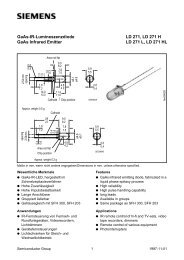
CNY75(G) Series Optocoupler with Phototransistor Output
CNY75(G) Series Optocoupler with Phototransistor Output
CNY75(G) Series Optocoupler with Phototransistor Output
- No tags were found...

Create successful ePaper yourself
Turn your PDF publications into a flip-book with our unique Google optimized e-Paper software.
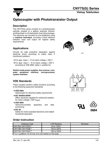
<strong>Optocoupler</strong> <strong>with</strong> <strong>Phototransistor</strong> <strong>Output</strong>DescriptionThe <strong>CNY75</strong>(G) series consists of a phototransistoroptically coupled to a gallium arsenide infraredemittingdiode in a 6-lead plastic dual inline package.The elements are mounted on one leadframe usinga coplanar technique, providing a fixed distancebetween input and output for highest safetyrequirements.<strong>CNY75</strong>(G) <strong>Series</strong>Vishay TelefunkenApplicationsCircuits for safe protective separation againstelectrical shock according to safety class II(reinforced isolation):14827 For appl. class I – IV at mains voltage ≤ 300 V For appl. class I – III at mains voltage ≤ 600 Vaccording to VDE 0884, table 2, suitable for:Switch-mode power supplies, line receiver, computerperipheral interface, microprocessorsystem interface.VDE StandardsThese couplers perform safety functions accordingto the following equipment standards: VDE 0884<strong>Optocoupler</strong> for electrical safety requirements IEC 950/EN 60950Office machines (applied for reinforced isolationfor mains voltage ≤ 400 V RMS ) VDE 0804Telecommunication apparatus and dataprocessing IEC 65Safety for mains-operated electronic and relatedhousehold apparatusOrder InstructionB C E6 5 41 2 3A (+) C (–) n.c.95 10805Ordering Code CTR Ranking Remarks<strong>CNY75</strong>A/ <strong>CNY75</strong>GA 1) 63 to 125%<strong>CNY75</strong>B/ <strong>CNY75</strong>GB 1) 100 to 200%<strong>CNY75</strong>C/ <strong>CNY75</strong>GC 1) 160 to 320%1) G = Leadform 10.16 mm; G is not market on the bodyRev. A4, 11–Jan–99 141
<strong>CNY75</strong>(G) <strong>Series</strong>Vishay TelefunkenFeaturesApprovals: BSI: BS EN 41003, BS EN 60095 (BS 415),BS EN 60950 (BS 7002),Certificate number 7081 and 7402 FIMKO (SETI): EN 60950,Certificate number 12399 Underwriters Laboratory (UL) 1577 recognized,file number E-76222 VDE 0884, Certificate number 94778VDE 0884 related features: Rated impulse voltage (transient overvoltage)V IOTM = 6 kV peak Isolation test voltage(partial discharge test voltage) V pd = 1.6 kV Rated isolation voltage (RMS includes DC)V IOWM = 600 V RMS (848 V peak) Rated recurring peak voltage (repetitive)V IORM = 600 V RMS Creepage current resistance according toVDE 0303/IEC 112Comparative Tracking Index: CTI = 275 Thickness through insulation ≥ 0.75 mmGeneral features: Isolation materials according to UL94-VO Pollution degree 2(DIN/VDE 0110 part 1 resp. IEC 664) Climatic classification 55/100/21 (IEC 68 part 1) Special construction:Therefore, extra low coupling capacity oftypical 0.3 pF, high Common Mode Rejection Low temperature coefficient of CTR CTR offered in 3 groups Coupling System AAbsolute Maximum RatingsInput (Emitter)Parameter Test Conditions Symbol Value UnitReverse voltage V R 5 VForward current I F 60 mAForward surge current t p ≤ 10 s I FSM 3 APower dissipation T amb ≤ 25C P V 100 mWJunction temperature T j 125 C<strong>Output</strong> (Detector)Parameter Test Conditions Symbol Value UnitCollector base voltage V CBO 90 VCollector emitter voltage V CEO 90 VEmitter collector voltage V ECO 7 VCollector current I C 50 mACollector peak current t p /T = 0.5, t p ≤ 10 ms I CM 100 mAPower dissipation T amb ≤ 25C P V 150 mWJunction temperature T j 125 CCouplerParameter Test Conditions Symbol Value UnitAC isolation test voltage (RMS) t = 1 min V IO 3.75 kVTotal power dissipation T amb ≤ 25C P tot 250 mWAmbient temperature range T amb –55 to +100 CStorage temperature range T stg –55 to +125 CSoldering temperature 2 mm from case, t ≤ 10 s T sd 260 C142Rev. A4, 11–Jan–99
<strong>CNY75</strong>(G) <strong>Series</strong>Vishay TelefunkenElectrical Characteristics (T amb = 25°C)Input (Emitter)Parameter Test Conditions Symbol Min. Typ. Max. UnitForward voltage I F = 50 mA V F 1.25 1.6 VReverse current V R = 6 V I R 10 AJunction capacitance V R = 0, f = 1 MHz C j 50 pF<strong>Output</strong> (Detector)Parameter Test Conditions Symbol Min. Typ. Max. UnitCollector base voltage I C = 100 A V CBO 90 VCollector emitter voltage I C = 1 mA V CEO 90 VEmitter collector voltage I E = 100 A V ECO 7 VCollector emitter cut-offcurrentV CE = 20 V, I F = 0 I CEO 150 nACouplerParameter Test Conditions Symbol Min. Typ. Max. UnitCollector emitter I F = 10 mA, I C = 1 mA V CEsat 0.3 Vsaturation voltageCut-off frequency V CE = 5 V, I F = 10 mA, f c 110 kHzR L = 100 Coupling capacitance f = 1 MHz C k 0.3 pFCurrent Transfer Ratio (CTR)Parameter Test Conditions Type Symbol Min. Typ. Max. UnitI C/IF V CE = 5 V, I F = 1 mA <strong>CNY75</strong>(G)A CTR 0.15<strong>CNY75</strong>(G)B CTR 0.3<strong>CNY75</strong>(G)C CTR 0.6V CE = 5 V, I F = 10 mA <strong>CNY75</strong>(G)A CTR 0.63 1.25<strong>CNY75</strong>(G)B CTR 1 2<strong>CNY75</strong>(G)C CTR 1.6 3.2Rev. A4, 11–Jan–99 143
<strong>CNY75</strong>(G) <strong>Series</strong>Vishay TelefunkenMaximum Safety Ratings (according to VDE 0884) see figure 1This device is used for protective separation against electrical shock only <strong>with</strong>in the maximum safety ratings.This must be ensured by using protective circuits in the applications.Input (Emitter)Parameters Test Conditions Symbol Value UnitForward current I si 130 mA<strong>Output</strong> (Detector)Parameters Test Conditions Symbol Value UnitPower dissipation T amb ≤ 25C P si 265 mWCouplerParameters Test Conditions Symbol Value UnitRated impulse voltage V IOTM 6 kVSafety temperature T si 150 CInsulation Rated Parameters (according to VDE 0884)Parameter Test Conditions Symbol Min. Typ. Max. UnitPartial discharge test voltage – 100%, t test = 1 s V pd 1.6 kVRoutine testPartial discharge test voltage – t Tr = 60 s, t test = 10 s, V IOTM 6 kVLot test (sample test)(see figure 2) V pd 1.3 kVInsulation resistance V IO = 500 V R IO 10 12 V IO = 500 V,R IO 10 11 T amb ≤ 100CV IO = 500 V,T amb ≤ 150CR IO 10 9 (construction test only)P tot – Total Power Dissipation ( mW )95 10923275250225200175150125100755025I si (mA)P si(mW)00 25 50 75 100 125 150 175T amb – Ambient Temperature ( °C)Figure 1. Derating diagramVV IOTMV PdV IOWMV IORM139300t 1t 1, t 2= 1 to 10 st 3, t 4= 1 st test= 10 st stres= 12 st Tr= 60 st 2t 4t 3t testt stresFigure 2. Test pulse diagram for sample test according toDIN VDE 0884t144Rev. A4, 11–Jan–99
<strong>CNY75</strong>(G) <strong>Series</strong>Vishay TelefunkenSwitching Characteristics of <strong>CNY75</strong>(G(AParameter Test Conditions Symbol Typ. UnitDelay time V S = 5 V, I C = 10 mA, R L = 100 (see figure 3) t d 2.0 sRise timet r 2.5 sFall time t f 2.7 sStorage time t s 0.3 sTurn-on time t on 4.5 sTurn-off time t off 3.0 sTurn-on time V S = 5 V, I F = 10 mA, RL = 1 k (see figure 4) t on 10.0 sTurn-off timet off 25.0 sSwitching Characteristics of <strong>CNY75</strong>(G)BParameter Test Conditions Symbol Typ. UnitDelay time V S = 5 V, I C = 10 mA, R L = 100 (see figure 3) t d 2.5 sRise timet r 3.0 sFall time t f 3.7 sStorage time t s 0.3 sTurn-on time t on 5.5 sTurn-off time t off 4.0 sTurn-on time V S = 5 V, I F = 10 mA, RL = 1 k (see figure 4) t on 16.5 sTurn-off timet off 20 sSwitching Characteristics of <strong>CNY75</strong>(G)CParameter Test Conditions Symbol Typ. UnitDelay time V S = 5 V, I C = 10 mA, R L = 100 (see figure 3) t d 2.8 sRise timet r 4.2 sFall time t f 4.7 sStorage time t s 0.3 sTurn-on time t on 7.0 sTurn-off time t off 5.0 sTurn-on time V S = 5 V, I F = 10 mA, RL = 1 k (see figure 4) t on 11 sTurn-off timet off 37.5 sRev. A4, 11–Jan–99 145
<strong>CNY75</strong>(G) <strong>Series</strong>Vishay Telefunken0I FR G= 50 t pT = 0.01t p= 50 s95 10891I F50 100 + 5 VI C= 10 mA ; Adjusted throughinput amplitudeChannel IChannel IIOscilloscopeR L 1 MC L 20 pFFigure 3. Test circuit, non-saturated operation100%90%96 11698I F0tt pI CI F0R = 50 GI F+ 5 VI C10%0t rt dt ont s t ftt pT = 0.01t = 50 s pt off14944501 k Channel IChannel IIOscilloscopeR L 1 M C L 20 pFpulse dura-delay timerise timeturn-on timet ptiont dt rt on (= t d + t r )t st ft off (= t s + t f )storage timefall timeturn-off timeFigure 4. Test circuit, saturated operationFigure 5. Switching timesTypical Characteristics (T amb = 25 C, unless otherwise specified)P tot – Total Power Dissipation ( mW )30025020015010096 1170050Coupled device<strong>Phototransistor</strong>IR-diode00 40 80 120T amb – Ambient Temperature (°C )Figure 6. Total Power Dissipation vs.Ambient TemperatureI F – Forward Current ( mA )1000.0100.010.096 118621.00.10 0.2 0.4 0.6 0.8 1.0 1.2 1.4 1.6 1.8 2.0V F – Forward Voltage ( V )Figure 7. Forward Current vs. Forward Voltage146Rev. A4, 11–Jan–99
<strong>CNY75</strong>(G) <strong>Series</strong>Vishay TelefunkenCTR rel – Relative Current Transfer Ratio1.51.41.31.21.11.00.90.80.70.6V CE =5VI F =10mA0.5–30 –20 –10 0 10 20 30 40 50 60 70 8096 11918 T amb – Ambient Temperature ( °C)Figure 8. Relative Current Transfer Ratio vs.Ambient TemperatureI C – Collector Current ( mA )95 110401001010.1V CE =5V0.010.1 1 10I F – Forward Current ( mA )100Figure 11. Collector Current vs. Forward CurrentI CEO – Collector Dark Current,<strong>with</strong> open Base ( nA )1000095 11038100010010V CE =30VI F =010 25 50 75T amb – Ambient Temperature ( °C )Figure 9. Collector Dark Current vs.Ambient Temperature100I C – Collector Current ( mA )95 11041100101<strong>CNY75</strong>A0.10.1 1 10I F =50mA20mA10mAV CE – Collector Emitter Voltage ( V )5mA2mA1mA100Figure 12. Collector Current vs. Collector Emitter VoltageI CB – Collector Base Current ( mA )10.10.010.0011 1095 11039V CB =5VI F – Forward Current ( mA )100Figure 10. Collector Base Current vs. Forward CurrentI C – Collector Current ( mA )95 11042100101I F =50mA<strong>CNY75</strong>B0.10.1 1 1020mA10mA5mA2mA1mAV CE – Collector Emitter Voltage ( V )100Figure 13. Collector Current vs. Collector Emitter VoltageRev. A4, 11–Jan–99 147
<strong>CNY75</strong>(G) <strong>Series</strong>Vishay TelefunkenI C – Collector Current ( mA )100.010.01.0I F =50mA20mA10mA5mA2mA1mA<strong>CNY75</strong>0.1C0.1 1.0 10.0 100.096 11919 V CE – Collector Emitter Voltage ( V)Figure 14. Collector Current vs. Collector Emitter VoltageV CEsat – Collector Emitter Saturation Voltage ( V )95 110341.00.80.60.40.210%01 10CTR=50%20%<strong>CNY75</strong>AI C – Collector Current ( mA )100Figure 15. Coll. Emitter Sat. Voltage vs. Coll. CurrentV CEsat – Collector Emitter Saturation Voltage ( V )95 110431.00.80.60.40.2<strong>CNY75</strong>BCTR=50%01 1010%20%I C – Collector Current ( mA )100Figure 16. Coll. Emitter Sat. Voltage vs. Coll. CurrentV CEsat – Collector Emitter Saturation Voltage ( V )95 110441.00.80.60.40.2<strong>CNY75</strong>C10%01 10CTR=50%20%I C – Collector Current ( mA )100Figure 17. Coll. Emitter Sat. Voltage vs. Coll. Currenth FE – DC Current Gain95 11035CTR – Current Transfer Ratio ( % )1000800600400200V CE =5V00.01 0.1 1 10I C – Collector Current ( mA )100Figure 18. DC Current Gain vs. Collector Current100010010<strong>CNY75</strong>A(G)V CE =5V10.1 1 1010095 11036I F – Forward Current ( mA )Figure 19. Current Transfer Ratio vs. Forward Current148Rev. A4, 11–Jan–99
<strong>CNY75</strong>(G) <strong>Series</strong>Vishay TelefunkenCTR – Current Transfer Ratio ( % )95 11045100010010<strong>CNY75</strong>B(G)V CE =5V10.1 1 10I F – Forward Current ( mA )100Figure 20. Current Transfer Ratio vs. Forward Currentt on / t off – Turn on / Turn off Time ( s )95 110485040302010<strong>CNY75</strong>B(G)Saturated OperationV S =5VR L =1k00 5 10 15I F – Forward Current ( mA )Figure 23. Turn on / off Time vs. Forward Currentt offt on20CTR – Current Transfer Ratio ( % )100010010<strong>CNY75</strong>C(G)V CE =5V10.1 1 1010095 11046I F – Forward Current ( mA )Figure 21. Current Transfer Ratio vs. Forward Currentt on / t off – Turn on / Turn off Time ( s )95 110505040302010<strong>CNY75</strong>C(G)Saturated OperationV S =5VR L =1k00 5 10 15I F – Forward Current ( mA )Figure 24. Turn on / off Time vs. Forward Currentt offt on20t on / t off – Turn on / Turn off Time ( s )5040302010<strong>CNY75</strong>A(G)Saturated OperationV S =5VR L =1k00 5 10 1595 11033I F – Forward Current ( mA )Figure 22. Turn on / off Time vs. Forward Currentt offt on20t on / t off – Turn on / Turn off Time ( s )2015105t ont off<strong>CNY75</strong>A(G)Non SaturatedOperationV S =5VR L =10000 2 4 6 895 11032I C – Collector Current ( mA )Figure 25. Turn on / off Time vs. Collector Current10Rev. A4, 11–Jan–99 149
<strong>CNY75</strong>(G) <strong>Series</strong>Vishay Telefunkent on / t off – Turn on / Turn off Time ( s )2015105<strong>CNY75</strong>B(G)Non SaturatedOperationV S =5VR L =10000 2 4 6 895 11047I C – Collector Current ( mA )Figure 26. Turn on / off Time vs. Collector Currentt ont off10t on / t off – Turn on / Turn off Time ( s )2015105t ont off<strong>CNY75</strong>C(G)Non SaturatedOperationV S =5VR L =10000 2 4 6 895 11049I C – Collector Current ( mA )Figure 27. Turn on / off Time vs. Collector Current10TypeDateCode(YM)XXXXXX918 A TK 630884VD EProductionLocationSafetyLogo15090CouplingCompanySystemLogoIndicatorFigure 28. Marking example150Rev. A4, 11–Jan–99
<strong>CNY75</strong>(G) <strong>Series</strong>Vishay TelefunkenDimensions of <strong>CNY75</strong>G in mmweight: ca. 0.50 gcreepage distance:air path: 8 mm 8 mmafter mounting on PC board14771Dimensions of <strong>CNY75</strong> in mmweight: 0.50 gcreepage distance:air path: 6 mm 6 mmafter mounting on PC board14770Rev. A4, 11–Jan–99 151