KBD-5 Keyboard
KBD-5 Keyboard
KBD-5 Keyboard

Create successful ePaper yourself
Turn your PDF publications into a flip-book with our unique Google optimized e-Paper software.
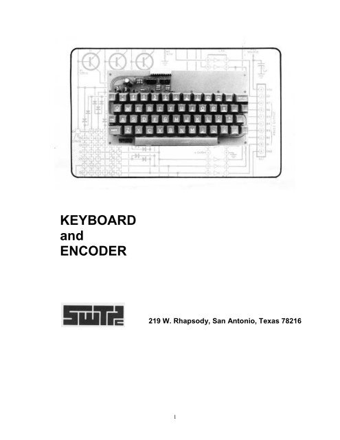
KEYBOARDandENCODER219 W. Rhapsody, San Antonio, Texas 782161
<strong>KBD</strong>-5 KEYBOARDGeneral DescriptionThe <strong>KBD</strong>-5 keyboard and ASCII encoder utilizes a single MOS integratedcircuit to perform the bulk of all necessary operations to generate full 8 bitparallel ASCII output code complete with a parity bit for error detection.Debounce is internal and automatic and choice between positive or negativekeypressed output strobe is provided. The keyboard can be programmed for uppercase characters only, or upper and lower case characters. The <strong>KBD</strong>-5 has thefeatures of n key lockout and 2 key rollover to help in reducing typing errors.Once a key is pressed pressing other keys will have no effect until the firstkey is released. The <strong>KBD</strong>-5 is already programmed for the control functions LINEFEED, RETURN and ESCAPE and can easily be programmed for other controlfunctions. The keyboard also has two SPST locking keyswitches which can be usedfor turning the RECEIVE, TRANSMIT and ECHO functions of a terminal such as theCT-1024 on and off. The keyboard also has an automatic repeat function whichcauses a string of characters to be transmitted after a key has been depressedfor more than about 0.5 seconds.Assembling your <strong>Keyboard</strong> and ASCII EncoderNOTE: MOS integrated circuits are susceptible to damage by staticelectricity. Although some degree of protection is provided internally withinthe integrated circuits, their cost demands the utmost in care. Before openingand/or installing any MOS integrated circuits you should ground your body andall metallic tools coming into contact with the leads through a 1M ohm 1/4 wattresistor (supplied with the kit). The ground must be an "earth" ground such as awater pipe, and not the circuit board ground. As for the connection to yourbody, attach a clip lead to your watch or metal ID bracelet. Make absolutelysure you have the 1M ohm resistor connected between you and the "earth" ground,otherwise you will be creating a dangerous shock hazard. Avoid touching theleads of the integrated circuits any more than necessary when installing themeven if you are grounded. On those MOS IC's being soldered in place, the tip ofthe soldering iron should be grounded as well (separately from your body ground)either with or without a 1 Meg ohm resistor. Most soldering irons having-a threeprong line cord already have a grounded tip. Static electricity should be an importantconsideration in cold, dry environments. It is less of a problem when itis warm and humid.( ) Install the 14 jumpers on the PC board. Use some of the light gauge wiresupplied with the kit or excess resistor leads. On the longer jumpers useinsulated wire to keep the jumper from shorting to other components.Jumpers are denoted on the circuit board by solid lines connecting twopads. As with all other component installation, unless otherwise noted,pull the jumpers down flush with the circuit board and solder.( ) Install the resistors and capacitors on the circuit board using thecomponent layout on the board and the parts list. Bend the leads over onthe back side of the board and trim so that 1/16" to 1/8" of lead remains.Solder.Scanned and edited by Michael Holley Mar 02, 2002 Revised May 23, 2003Southwest Technical Products Corporation Document Circa 19751
( ) Install integrated circuits IC2-IC3 on the board, Be sure to orient theIC's as shown on the board and do not bend the leads on the back side ofthe board. Doing so makes it very difficult to remove the IC shouldreplacement ever be necessary. Do not install IC1 at this time. Solder.( ) Install the transistor and diodes on the board. Leave about 1/4" clearancebetween the transistor body and the circuit board. Be sure to orient thecomponents exactly as shown on the component side of the board. Solder.( ) Check the key switches with an ohmmeter before they are installed to besure that they are making contact properly and to be sure that they do notstick. Solder the switches in place one at a time using as little heat asnecessary to get a good solder joint. Note that the keyswitches for theRCVE/XMIT and ECHO positions are a SPST switch and are different from therest. The switches can be recognized by pressing each keyswitch. The SPSTswitches will have a locking position. Install these two switches first.Be careful not to force any switch into a hole in such a way as to damagethe connecting wires. Excessive heating can distort, or even melt theplastic body and ruin the keyswitch. Check the switch again with anohmmeter for proper operation after soldering it in place. This can savemuch troubleshooting later. If the switch works properly heat stake theswitch in place by melting over the ends of the plastic mounting bosses.This can be done with the tip of your soldering iron.After all keyswitches have been installed and checked you are ready toinstall the programming strips on the bottom of the board. These stripsmount vertically, at right angles to the main board. The etched finger,connection points on the programming strips will match the connection padson the main board when the strips are in the correct position. Hold one ofthe strips in the correct position and turn it so that the connectionfingers match the pads on both sides of the strip. Note that there are twoways the strip may be turned and only one is correct. If the strips edgeis too rough to fit down solidly against the main board, file, or sandthat edge flat. Hold, or clamp sides of the strip to the main board, pads.Install the other strip in the same way. Both strips are identical.( ) The spacebar and equalizer assembly goes together as follows. Mount akeyswitch on the board in the center of the spacebar area. Mount the two"L" shaped brackets with a notch in the top on each side of the keyswitchin the holes provided. The side of the bracket with the notch should benext to the circuit board edge. These should be fixed in place by meltingand flattening slightly the plastic pins on the back of the board withyour soldering iron tip. Press one of the equalizer wire retainers intoplace on the end of the spacebar itself. The hole for the wire should beon the more slanted side of the spacebar that has the four casting bumps.Slip the equalizer wire into the hole in, the retainer you have not yetpressed into place. Press the second retainer into place. Turn thespacebar upside down in front of the board and press the equalizer wireinto the notches in the top of the mounting clips. Turn the spacebar overand position it over the keyswitch in the center of the board. Press itdown into place.2
( ) Install IC1 following the precautions given for MOS IC's. Solder.( ) To finish the keyboard assembly snap the plastic key tops on theirrespective keyswitch as noted on the key configuration drawing. If some ofthe keytops are loose you can securely fasten them to the switches byusing a small amount of plastic cement. Blank keytops may be supplied forthe RCVS/XMIT and ECHO positions.The programming of the "CASE", "PARITY" and the "KEYPRESSED" jumpersdepends on what your keyboard will be used for. For upper case characters onlyconnect a jumper from the pad marked "CASE" to "U". For upper plus lower caseconnect the jumper from the "CASE" pad to "U + L". For a positive keypressedstrobe (KP line normally low, goes high when a key is pressed) connect a jumperfrom the KP pad to "+", for a negative keypressed strobe (KP line normally high,goes low when a key is pressed) connect a jumper from the KP pad to "-". Ajumper for "PAR" should also be installed to its respective "U" or "U + L" paddepending on whether upper case or upper plus lower case characters will beused.Notice to CT-1024 Terminal OwnersIn order for the <strong>KBD</strong>-5 to be used on the CT-1024 terminal the keyboardshould be programmed for a negative keypressed strobe (KP select jumper connectedto -) and for upper case characters only, ("CASE" jumper connected to U).This is the normal programming for other TV TYPEWRITERS but may need to bemodified for your particular application. The parity bit is not used in theCT-1024 but the "PAR" jumper should be connected to "U". The terminals R, T andE of J1 can be connected to control the receive/transmit and echo functions ofyour CT-1024 if a serial interface is installed. Connect R to JS-1 pin 5, T toJS-1 pin 4 and E to JS-1 pin 8 of the serial interface.CheckoutThe only equipment needed to check the operation of your keyboard is a DCmilliammeter and a DC voltmeter. Apply +5 volts, ground, and -12 volts to theproper pins and check for currents of about 4 mA on the -12 line and about 8mAon the +5 line (no keys pressed). If the currents are much higher than this stopimmediately and check for parts inserted incorrectly or solder bridges. If thecurrents check OK check the keypressed output. If the KP select jumper is setfor (-) the KP output should be high (4.5V nominal) and go low (0.1 voltsnominal) when a key is pressed. If the KP output is held low check for possiblesolder bridges or a shorted key switch. If the KP select jumper is set for (+)the KP output will be normally low and will go high when a key is pressed. Ifall seems well refer to the ASCII code tables supplied and check the outputs ofbits 1-7 with-your voltmeter for each individual character. Be sure to use thecorrect table depending on how the "CASE" selector is wired on your keyboard.With the "CASE" selector set for the upper case only the SHIFT control will haveno effect on the output code when any letter is pressed but will make bit 5 a 0when any character of column 3 of Table 1 is pressed. When in the upper caseonly mode the SHIFT key will not affect any of the characters in columns 4 or,5.Pressing the control key forces bit 7 to be a 0 therefore allowing you to selectthe operators in columns 0 and 1. When in the upper plus lower case mode theSHIFT key makes bit 6 a 1 when letters of columns 4 and 5 of table 2 are pressedand makes bit 5 a 0 when any character of column 3 is selected. The control keyoperates as before.3
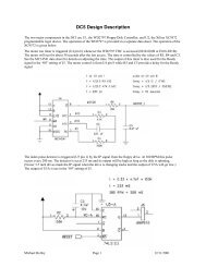
This keyboard uses EVEN parity in both the upper case only and the upperplus lower case modes. The parity bit should be low when the number of zeros inthe output code is odd and should be high when the number of zeros is even. Forexample the ASCII code for X, 0001101, should make the parity bit high. Therepeat function should be checked by holding any one key down for more thanabout 1 sec. The keypressed strobe should switch on and off until the key isreleased. If a faster or slower repeat rate is desired the value of C6 can bechanged slightly.Circuit DescriptionAs shown in figure 1 the keyswitches are arranged into a matrix with the Xlines from IC-1 outputting test pulses in time sequence and the Y lines sensingtheir presence. If no key is pressed, IC-1 continuously scans the keys, at arate of 50,000 keys per second. Whenever a key is closed, the scanning actionstops and that location is held by the internal circuitry of the encoder. Thislocation is called an address. This address is routed to an internal fixedmemory called a read only memory. In exchange for an address and someinformation on the status of the shift and control keys the read only memorygives the proper 8 bit ASCII output code, complete with parity.As soon as the scanning stops, a time delay is started and controlled byR1 and C1. This takes into account any switch closure bounce or noise and makessure the key is firmly down and not just brushed on the way by. After the delaytime, an output "keypressed" strobe is made available. This tells whatever youattach to your keyboard that the code is ready for use and valid.If a key is released the scanning action starts up again and goes on tilla new key is pressed. If two keys are pressed at nearly the same time the firstkey pressed provides its output code after a debounce delay. When the first keyis released, the scanner starts up but only goes around till it hits the otherkey's location. After a new debounce delay, the second key's code is output.Keys can continue to be pressed in sequence two down at a time forever, withalways the right code being output in sequence, and nothing missed or out oforder. This most handy feature takes care of sloppy typing and "burst" ratetyping where keys are hit fast and furious in sequence.IC2 and IC3 are used for the automatic repeat function. IC3 is setup as anastable multivibrator that continuously runs at a frequency of approximately 8.5Hz. When a key is first pressed the KP line of IN goes high causing an immediatelow output of IC2-C. If the key is immediately released no repeat function isinitiated. If the key is held down for more than about 1 second C7 will chargeto a point where IC2A is triggered. At this time the output of IC3 is NAND'edwith the KP strobe therefore causing the KP signal to be chopped just as if thekey was continuously pushed and released. This action will continue until thekey is released.4
In Case of ProblemsThe tests called for in the check-out procedure are designed to warn youof problems before they can cause damage. If any abnormal results are obtainedduring the tests, or if there is obvious overheating of any part discontinue useuntil the problem is located and corrected. Experience has shown that mostproblems are caused by minor wiring, component installation and solderingtechnique errors which can be prevented by careful assembly.If you do have problems with your keyboard there are several tests you canperform which may help you locate the problem. You will need an ohmmeter, anoscilloscope, and a DC voltmeter for these tests. First go back and check oncemore for proper component installation and for solder bridges or cold solderjoints. Also be sure that the correct jumpers are in place. Next check eachkeyswitch with an ohmmeter to be sure none are shorted. If you have anoscilloscope apply power to the keyboard and check for a 50 KHz signal on pin 40of IC-1. If you obtain no signal check for 5 volts on pin 1, -12 on pin 18 andground on pin 17.Repair ProcedureRepairs will be made on a basic rate charge plus parts. The basic rate forthe <strong>KBD</strong>-5 is $10.00. If you must return your <strong>KBD</strong>-5 please send the $10.00-in theform of a money order or cashiers check along with the keyboard. When repairsare finished the keyboard will be returned to you COD for parts charges, if any.Do Not send personal checks for repair work.Pack all parts to be returned carefully and insure. We will not acceptdelivery on any parcels that arrive in damaged condition. Make check or moneyorder payable to Southwest Technical Products Corporation.5
Parts List - <strong>KBD</strong>-5 <strong>Keyboard</strong>R1R2R3R4R5R6R7Resistors680K ohm 1/4 watt resistor100K ohm 1/4 watt resistor150K ohm 1/4 watt resistor47K ohm 1/4 watt resistor10K ohm 1/4 watt resistor680 ohm 1/4 watt resistor330 ohm 1/4 watt resistorCapacitorsC1, C5 0.01 mfd disc capacitorC247 pf polystyrene capacitorC3, C4 0.1 mfd @16 volt disc capacitorC60.47 mfd tantalum capacitorC7220 mfd @6.3 volt electrolyticcapacitorICIIC2IC3Q1Dl - D3J1S1-S2S3-S56Semiconductors2376 <strong>Keyboard</strong> Encoder (MOS)74LS00 quad NAND gate555 timer2N5210 NPN silicon transistor1N4148/1N914 silicon diodeMisc.15 pin Molex edge connector<strong>Keyboard</strong> switch, SPST locking<strong>Keyboard</strong> switchPC board, programming jumpers (2),Keytops6
BIT NUMBERSb7 b6 b5 b4 b3 b2 b1b7b6b5COLUMNROW0000010100 1 2 3 4 50 0 0 0 0 NUL DLE SP 0 @ P0 0 0 1 1 SOH DC1 ! 1 A Q0 0 1 0 2 STX DC2 “ 2 B R0 0 1 1 3 ETX DC3 # 3 C S0 1 0 0 4 EOT DC4 $ 4 D T0 1 0 1 5 ENQ NAK % 5 E U0 1 1 0 6 ACK SYN & 6 F V0 1 1 1 7 BEL ETB ‘ 7 G W1 0 0 0 8 BS CAN ( 8 H X1 0 0 1 9 HT EM ) 9 I Y1 0 1 0 10 LF SUB * : J Z1 0 1 1 11 VT ESC + ; K [1 1 0 0 12 FF FS , < L \1 1 0 1 13 CR GS - = M ]1 1 1 0 14 SO RS . > N ^1 1 1 1 15 S1 US / ? 0 _011100101Available codes and characters for the UPPER CASE modeAY-5-2376 <strong>Keyboard</strong> EncoderBIT NUMBERSb7 b6 b5 b4 b3 b2 b1b7b6b5COLUMNROW0000010100110 1 2 3 4 5 6 70 0 0 0 0 NUL DLE SP 0 @ P \0 0 0 1 1 SOH DC1 ! 1 A Q a q0 0 1 0 2 STX DC2 “ 2 B R b r0 0 1 1 3 ETX DC3 # 3 C S c s0 1 0 0 4 EOT DC4 $ 4 D T d t0 1 0 1 5 ENQ NAK % 5 E U e u0 1 1 0 6 ACK SYN & 6 F V f v0 1 1 1 7 BEL ETB ‘ 7 G W g w1 0 0 0 8 BS CAN ( 8 H X h x1 0 0 1 9 HT EM ) 9 I Y i y1 0 1 0 10 LF SUB * : J Z j z1 0 1 1 11 VT ESC + ; K [ k {1 1 0 0 12 FF FS , < L \ l |1 1 0 1 13 CR GS - = M ] m }1 1 1 0 14 SO RS . > N ^ n ~1 1 1 1 15 S1 US / ? 0 _ o DEL100101110111Available codes and characters for the UPPER PLUS LOWER CASE modeAY-5-2376 <strong>Keyboard</strong> Encoder7
CONNECTX0 X1 X2 X3 X4 X5 X6 X7TO OBTAIN39 38 37 36 35 34 33 32NORMAL NUL DLE - 0 ; l o 9Y0 SHIFT NUL DLE = NUL + L O )31 CONTROL NUL DLE NUL NUL NUL FF SI NULNORMAL SOH K FS : / k i 8YI SHIFT SOH [ FS * ? K I (30 CONTROL SOH VT FS NUL NUL VT HT NULNORMAL STX L GS p . j u 7Y2 SHIFT STX \ GS P > J U ‘29 CONTROL STX FF GS OLE NUL LF NAK NULNORMAL ETX N RS _ , h y 6Y3 SHIFT ETX ^ RS DEL < H Y &28 CONTROL ETX SO RS US NUL BS EM NULNORMAL EOT M US @ m g t 5Y4 SHIFT EOT ] US ` M G T %27 CONTROL EOT CR US NUL CR BEL DC NULNORMAL ENQ NAK < BS n f r 4Y5 SHIFT ENQ NAK < BS N F R $26 CONTROL ENQ NAK NUL BS SO ACK DC NULNORMAL ACK SYN > [ b d e 3Y6 SHIFT ACK SYN > { B D E #25 CONTROL ACK SYN NUL ESC STX EDT ENQ NULNORMAL BEL ETB , ] v s w 2Y7 SHIFT BEL ETB , { V S W "24 CONTROL BEL ETB NUL GS SYN DC ETB NULNORMAL DC1 CAN SP CR c a q 1Y8 SHIFT DC1 CAN SP CR C A Q !23 CONTROL DC1 CAN SP CR ETX SOH DC1 NULNORMAL P EM . LF x FF HT ^Y9 SHIFT @ EM . LF X FF HT ~22 CONTROL DLE EM NUL LF CAN FF HT RSNORMAL 0 SUB _ DEL z ESC VT \Y10 SHIFT _ SUB _ DEL Z ESC VT :21 CONTROL SI SUB US DEL SUB ESC VT FS8
<strong>Keyboard</strong> ModificationsThese are the modifications that I did on my CT-1024 SystemBack SpaceThe backspace key is not connected to anything. To generate a BS(08)connect a wire from one pin of the key switch to Y5 (IC1 pin 26). Connect a wirefrom the other pin of the key-switch to X3 (IC1 pin 36).At Sign @To generate an at sign "@" you can change the function of the letter Pkey. Isolate both pins of the P key-switch. Cut the trace going to the left pinnear the switch. Cut the trace for the right pin on both sides of the pin. Youwill need jumper the right trace around the switch.Connect a wire from the left pin of the key-switch to Y9 (IC1 pin 22).Connect a wire from the other pin of the key-switch to X0 (IC1 pin 39).When the shift key is held down the P key will send an @.UnderscoreTo generate an under score "_" you can change the function of the letter Okey. Isolate both pins of the O key-switch. Cut the trace on the vertical stripnear the switch (between the O and I switch). Cut the trace for the right pin onboth sides of the pin. You will need jumper the right trace around the switch.Connect a wire from the left pin of the key-switch to Y10 (IC1 pin 21).Connect a wire from the other pin of the key-switch to X0 (IC1 pin 39).When the shift key is held down the O key will send a _.11