Exciting Opportunities for Nanotechnology R & D and - Arizona ...
Exciting Opportunities for Nanotechnology R & D and - Arizona ...
Exciting Opportunities for Nanotechnology R & D and - Arizona ...

You also want an ePaper? Increase the reach of your titles
YUMPU automatically turns print PDFs into web optimized ePapers that Google loves.
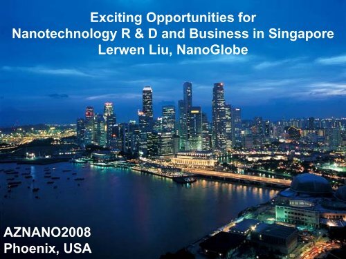
<strong>Exciting</strong> <strong>Opportunities</strong> <strong>for</strong><strong>Nanotechnology</strong> R & D <strong>and</strong> Business in SingaporeLerwen Liu, NanoGlobeAZNANO2008Phoenix, USA
About Singapore
Nanotech in Macro Regional <strong>Opportunities</strong>7 hour geographyIndia:population 1.1 billionreal GDP growth = 9.4% (2006)Japan:population 127.4 millionChina:real GDP growth = 2.2% (2006)population 1.32 billionreal GDP growth = 11.1% (2006)•1 hour2 hours3 hoursASEAN:population 560 millionreal GDP growth = 6% (2006)• Fastest EconomicGrowth Region• Large Markets – 3.3billion people• HQ <strong>for</strong> Asia NanoForum (ANF,www.asia-nano.org)• Efficient Government• Multi-cultural• Tropical climate• Resort living life style4 hours5 hours6 hours7 hoursAustralia:population 20millionreal GDP growth = 2.5% (2006)
Singapore’s s economic progressInnovator ofnew products& servicesSkills-intensiveLabour-intensiveCapital-intensiveTechnology-intensiveKnowledge-Intensive1960 GDP = S$ 2 bn 2006 GDP = S$ 210 bn!
Singapore Economic SnapshotConstruction4%Others17%Wholesale& Retail15% Transport &Communications13%Manufacturing28%BusinessServices12%Biomedicals Mfg25%FinancialServices11%2006 GDP: S$210 billionGDP Growth: 7.9%Mechanical Engrg24% General MfgIndustries9%Manufacturing VA by sector:Still key contributor to GDPChemicals14%Electronics28%
Singapore’s s Value PropositionStrong Govt SupportRobust R&D Network• Public R&D Centres (IMRE,IBN, IME)• World-class UniversitiesStrong IP Protection• Ranked #1 in Asia• Incentives• Facilitation• Fast to ImplementExcellent Stability• Ranked lowestpolitical risk in AsiaLogistically Connected• Top air cargo hub in Asia• World’s largesttransshipment portSkilled Manpower• Talent pool fromlocal Universities,Polytechnics <strong>and</strong> fromthe regionEase of AttractingForeign Talent• High st<strong>and</strong>ard of living• Low personal income tax<strong>and</strong> corporate taxVibrant Private Sector• Companies from allparts of value chain• Comprehensiveecosystem
Singapore R&D SystemNationalResearchFoundationMinistries Trade & Industry Education HealthDefenseCRP, CREATE,RCER&DFundingBodiesEDB A*STARAcademicResearchNMRCDSTAFundR&DPer<strong>for</strong>mersIndustryA*STARResearchInstitutesUniversitiesHospitalsDSONationalLaboratories
Government Industry SupportAgency <strong>for</strong> industry development,<strong>for</strong>eign investment attractionMinistry ofTrade &IndustryPromotion of international trade &internationalisation of Singapore-basedenterprisesChampion <strong>for</strong> enterprise development.National body <strong>for</strong> productivity, st<strong>and</strong>ards<strong>and</strong> con<strong>for</strong>manceEnsure supply of industrial facilities <strong>and</strong>industrial spaceDevelop Singapore’s researchcapabilities.Promote <strong>and</strong> develop tourism industry.Regulate energy providersDevelop <strong>and</strong> promote Sentosa Isl<strong>and</strong>.Regulate anti-competitive activities.
Significant Increase in R&DFunding1614S&T2010$13.55 bil12Investing in R&D$ Billion10864NTP$2 bilNSTP$4 bilS&T2005$6 bil201991 1996 2001 2006Target – Increase GERD to 3% GDP by 2010
Incentives SME <strong>and</strong> Start Ups in NanotechASTAR (Agency <strong>for</strong> Science, Technology <strong>and</strong> Research)Labs in RI Model(Share resources <strong>and</strong> man power)T-UP Program (Technology Upgrade, 70% funded manpowerP3 Research Program (Plastics Electronics)SPRING (St<strong>and</strong>ards, Productivity <strong>and</strong> Innovation Board)Equity Financing Scheme (SEEDS- 300K matching 3 rd party investment)TIP Program (Technology Innovation Program, 50% support)TIP Version 2 program (50M/5Y,Phase 1: 250K, Phase 2: 500K-To launch inApril08)Business Angel Scheme (1:1 matching up to 1M)EDB (Economic Development Board)Innovation Development Scheme (IDS)Research Incentive Scheme <strong>for</strong> Companies (RISC)Strategic Attachment <strong>and</strong> Training (STRAT)Incentives In New Technology (INTECH)Patent Support Grant (up to 20K)
SPRING Technology EnterpriseCommercialisation Scheme (TECS)• Based on US Small Business Innovation Research (SBIR) & SmallBusiness Technology Transfer (STTR) programmes• Aims to overcome high risks involved in commercialisation of new“quantum-leap” R&D ideas encourage <strong>for</strong>mation of technology startups• S$50 mil fund over 5 years• 2 phases of funding:(i) Phase I: up to S$250,000 to demonstrate proof-of-concept of acommercialisable idea(ii) Phase II: up to S$500,000 on 85% co-sharing basis <strong>for</strong> further R&D.Only Phase I winners considered
R & D Infrastructures(Science Park I, II <strong>and</strong> III,biopolis, Fusionpolis,Network)
BiopolisThe Biomedical Hub of AsiaPhase 3Phase 2Phase 3 Phase 3Phase 1 – 185,000 sqm (2003-) Phase 1 – 120,000 sqm (2008-)Phase 2 – 28,000 sqm (2006-) Phase 2A – 103,600 sqm (2010)Phase 3 – Planning begins in 2007 Phase 2B – 50,000 sqm (2010)
SCIENCE MEETS BUSINESS AND THE ARTSWill house the Science & Engineering Research Council (SERC)research institutesAim is to Foster innovation, experimentation <strong>and</strong> collaborationIncubator <strong>for</strong> next generation applications <strong>and</strong> technologies.Facilities available at Fusionopolis include‣ Testbed from R&D stage to trial deployment‣ 1-stop-shop <strong>for</strong> high end computing <strong>and</strong> IT needs‣ High per<strong>for</strong>mace computing‣ Network storagehttp://www.fusionopolis.com/pages/centralXchange/index.asp
NanoFabrication &Characterisation FacilityA network of nanofabrication <strong>and</strong>characterisation facilities(http://www.imre.a-star.edu.sg/rnd/SNFC.asp)
Nanofabrication <strong>and</strong> CharacterisationFacility• Provide easy access to world class researchfacilities (equipment <strong>and</strong> clean room) <strong>for</strong>nanofabrication <strong>and</strong> characterisation• Initially at IMRE, but will be exp<strong>and</strong>ed to otherRIs <strong>and</strong> Universities onlyOLED relatedLitrex printer, spinner, oven,Thermal EvaporatorNano Fabrication Facilities• Available <strong>for</strong> use by all researchers• Use of equipment individually or asprocess• Use reserved through one web-site(https://tetra.simtech.a-star.edu.sg/rbs/)III-V relatedE-Beam Evaporator, PECVD, ICP,Holographic System, RTP, MOCVDQuartz/silicon relatedICP, RIE, LPCVDSilicide relatedRTP, Sputtering, PECVD700 sq m of clean roomsupporting nanofabricationat IMREFerroelectric relatedRTP, etching systemPolymer relatedNano-imprinter, pressSurface Characterisation‣ XPS‣ ToF-SIMS‣ Scanning ProbeMicroscopy‣ Dynamic SIMSMaterials Characterisation FacilitiesMechanics LabMicrostructural CharacterisationChemical & Polymer Characterisation‣ Nanoindentation‣ HR-TEM‣ NMR (400 MHz, MAS)‣ High precision mechanical ‣ SEM / HR-SEM‣ Spectroscopictesting‣ XRDs (powder,Ellipsometry‣ Other mechanical testingtexture, 2D‣ FTIR, DSC, TGA‣ Mechanical Modellingdetection)
Nanotech R & D Strength
R&D: Why Singapore?• Gross Expenditure on R&D – 2.39% of GDP• More than 22,600 Research Scientists & Engineers• 102 researchers per 10,000 work<strong>for</strong>ce*Manufacturing Electronics Chemicals &MaterialsIMESIMTechDSIIHPCIMRE ICESIMCBBTCGIS IBN BII I 2 RBiomedicalSciencesIn<strong>for</strong>mation &CommunicationsSIMTechIMEIHPCDSII 2 RICESIMREIMCBBTCGISBIIIBN- Singapore Institute ofManufacturing Technology- Institute of Microelectronics- Institute of HighPer<strong>for</strong>mance Computing- Data Storage Institute- Institute <strong>for</strong> Infocomm Research- Institute <strong>for</strong> Chemical &Engineering Sciences- Institute of MaterialResearch & Engineering- Institute of Molecular <strong>and</strong> Cell Biology- Bioprocessing Technology Centre- Genome Institute of Singapore- Bioin<strong>for</strong>matics Institute- Institute of BioEngineering &<strong>Nanotechnology</strong>*Source: National Survey of R&D in Singapore 2006, Agency <strong>for</strong> Science, Technology <strong>and</strong> Research (A*Star), 2006
Nanotech R&D in SERCInstitute of MaterialResearch & EngineeringInstitute of ChemicalEngineering & SciencesData StorageInstituteInstitute ofMicroelectronicsInstitute of HighPer<strong>for</strong>mance ComputingSingapore Institute ofManufacturing TechnologyAtomistic modeling Catalysismolecular manipulationNanobiomimeticsSpintronicsNanoElectronicsMolecular selfassemblyChemical processtechnologyMultifunctionalcoatings,membranesOrganic & polymerelectronicsMEMS NEMSAdvanced NanomaterialsNanoimprintingQuantum DotsNanomachining
IME 200mm Si-Based Wafer Processing <strong>and</strong> MEMS Prototyping FacilityDeep UV LithographySEM defect reviewMicro & Nano-Electronics• Diffusion / LPCVD furnaces• SiGe epitaxy (UHVCVD)• ALCVD <strong>for</strong> high k / metal gate &interconnects barrier• Ion implanter• Wafer Cleaning• RTA <strong>for</strong> S/D spike <strong>and</strong> metal/silicide• Metallization•Metal PVD <strong>for</strong> Gate / Barrier / Silicide•W (Tungsten) plug CVD•PVD <strong>for</strong> barrier <strong>and</strong> Cu -interconnects• Lithography •Cu electroplating <strong>for</strong> interconnects• 248 nm DUV• E-beam Lithography• Dielectric (low-K) Deposition• Plasma etch <strong>for</strong> poly-Si,dielectric, metal• CMP <strong>for</strong> oxide, W, <strong>and</strong> Cu• In-line metrology/AnalysisMEMS & Post-CMOS• Double sided contact / proximityaligner• Wafer bonder• High pressure bonding (Thermocompression,Anodic <strong>and</strong> Frit glassbonding)• Plasma deep Si etch• Wet TMAH/KOH etching• Electroplating <strong>for</strong> Cu, Ni, Au,photoresist• Wafer thinning & polishingSiGe UHVCVD epitaxyR&D Foundry <strong>for</strong> micro-, nano-, bio- <strong>and</strong> optoelectronics
Wafer Process <strong>and</strong> Package Assembly Characterization‣ Advanced analytical & test tools <strong>for</strong>: structure / surface analysis,device / package assembly diagnostics <strong>and</strong> reliability characterization‣ More than 800 jobs <strong>and</strong> investigative projects per<strong>for</strong>med <strong>for</strong> local MNC,SME <strong>and</strong> universities per yearFIBD - SIMSAFMM-STEM/EELS/HolographyX-ray imagingESDSAMProbe StationsTEM/EDXSEM/EDXFEAUGERIME’s collaborator facilitiesTOF-SIMSWet-chemicalAnalysisScanningAnalytical PEMFTIRGC-MSDSC/DTA/TMA/TGAReliabilityChambersXPS
Focus Area: Si-NanowireTechnology‣ Establish CMOS-compatible Si-nanowire device <strong>and</strong> technologyplat<strong>for</strong>m‣ Facilitate applications in: Low-Power Logic Circuits, HighPer<strong>for</strong>mance Memories, Wire-based SensorsE. Gnani et al. / Univ Bologna, ESSDERC’06
CMOS-compatible Si Nanowire Array<strong>for</strong> Biomedical Application• Silicon nanowires offer high surface-to-volume ratio<strong>and</strong> hence increased sensitivity of detection throughconductance change• Silicon nanowires can be functionalized to detectcancer biomarkers <strong>and</strong> other biomolecules such asvirus <strong>and</strong> sequence-specific DNA5 nm thick SiNW in SiO2HRTEM image of Si Nanowireembedded in SiO 2Gate Poly Silicon4 nm thickSiO 2Fluidicflow path≤3 nm thick SiNW2 μmMetalelectrode MetalelectrodeFluidicFluidic channelchannel sidewallsidewallSi Nanowire Array <strong>for</strong> Bio-sensors
Focus Area: Photonics‣ Establish CMOS-compatible monolithic technology plat<strong>for</strong>m <strong>for</strong>OEICTransmittercircuits‣ Bi-Directional optical-interconnects onPCB10 Gbps Tcvr 10 Gbps TcvrModuleModuleReceivercircuitsBi-Directional Optical link on FR4 PCB
MEMS at IMEThe MEMS (Micro-Electro-Mechanical Systems) R&D programme in IME started as far back as1993.We have developed integrated research capabilities <strong>for</strong> MEMS, including MEMS design,Application Specific Integrated Circuit (ASIC) design, process development <strong>and</strong> custompackage development.We have developed many cost-effective MEMS products <strong>and</strong> devices such as integratedpressure sensor, accelerometer, micro-relay, ISFET immunosensor, micro-PCR <strong>and</strong>micro-CE, <strong>and</strong> IR bolometer.Several of these devices have been successfully commercialized.Silicon tipsMicromirrorHDD actuatorMicro-relayRF resonatorVacuum sealedbolometer30:1 highaspect ratio SiCantileversinside bio-wellsSiliconaccelerometerμPCR <strong>for</strong> DNAamplification
• Double sided contact / proximity alignerMEMS-Specific ProcessesAvailable• Wafer track <strong>for</strong> coating thick resist <strong>and</strong> Polymers• Spin coating of thin/thick resists• Photo/non-photo sensitive BCB coating• Wafer to wafer bonding• fusion pre- bonding/alignment• anodic bonding• frit glass bonding• polymer bonding• Eutectic <strong>and</strong> Solder bonding• Metal to metal thermal-compression bonding• Low-temperature hermetic bonding• Bulk Si-micromachining• Deep Reactive Ion Etching• Wet TMAH/KOH etching• 3 <strong>and</strong> 4 terminal electrochemical etch• Surface micromachining• RIE/wet etching of polysilicon, Silicon Nitride,Silicon dioxide, Aluminum <strong>and</strong> other thin films (CMOS compatible tools, however separate toolsneeded to avoid contamination issues)• Release etching process• XeF2 <strong>and</strong> SF6 Silicon release etch• HF vapor release etch of silicondioxide• Electroplating <strong>for</strong> Cu, Ni, Au, photoresist• Wafer thinning & polishing• Wafer grinder/polisher• Thin/thick film deposition• Low stress/controlled stress films suchas polysilicon, silicon nitride, <strong>and</strong>silicon dioxide• Thick dielectric films 5-10μm• Metallization• e-beam evaporation <strong>and</strong> PVD• Al, AlSi, Cu, Au, Chromium, refractive<strong>and</strong> rare-earth metals• Ti/TiN <strong>and</strong> TaN barrier metallization• Supercritical CO 2drying• Self assembling monolayer coating <strong>for</strong>anti-stiction• Bio-compatible polymer microstructurefabrication- PDMS, parylene
Mech EngrgElect Comput EngrgChem Env EngrgCivil EngrgBioengrgBiologyMedicineBiochemistryNanotech R&D in NUS <strong>and</strong> NTUNUS NNINanoscience <strong>and</strong><strong>Nanotechnology</strong>InitiativePhysicsMaterials ScienceMathematicsChemistryResearch• Nanobioengineering• Nanoelectronics• Nanophotonics• Nanomagnetics & Spintronics• Nanofiber science &engineering• Nano- micro-fabricationCross-facultyjoint researchcollaborationsNano-Magnetics &photonicsOrganic,MolecularElectronicsNTU NanoclusterNanoscience <strong>and</strong><strong>Nanotechnology</strong>Clusterhttp://www.ntu.edu.sg/nanocluster/NanoTechApplnsEnergy &CatalysisNanodevicesNano-Materials:SynthesisNanobiotech
<strong>Nanotechnology</strong> R&D in UniversitiesNational University of Singapore (NUS):Nanoscience <strong>and</strong> <strong>Nanotechnology</strong> Initiative (NUSNNI)‣ Involves some 189 faculty <strong>and</strong> research staff from 20 research labs around NUS;working on some S$17 million worth of research grants per year.‣ Nanoscience - molecular self-assembly <strong>and</strong> devices, nano-structure <strong>for</strong>mation,<strong>and</strong> in-situ nano-characterisation instrumentation‣ <strong>Nanotechnology</strong>- photonics, silicon nanodevices, in<strong>for</strong>mation storage materials,quantum computing, spintronics, Graphene, nanoscale materials <strong>and</strong> systems,bio-nanotechnology‣ Solar Energy Research Institute (130MSGD/5Y funed by EDB) <strong>and</strong> QuantumIn<strong>for</strong>mation Science <strong>and</strong> Technology (150MSGD/5Y funded by NRF)Nanyang Technological University (NTU):Nanoscience <strong>and</strong> <strong>Nanotechnology</strong> Cluster (NanoCluster)‣ Close to 90 faculty members from all disciplines of science & engineering‣ Wide network of research centres with shared facilities <strong>for</strong> nanofabrication,nanocharacterization, <strong>and</strong> exploitation of nanotechnologies. MEMS R & DFoundry Services‣ Key areas: Microelectroncs & Photonics, MEMS, Precision Engineering, AdvancedMaterials, Analysis & Characterization, Testing & Simulation
Driving CommercializationReady Partners within 250 sq milesMulti-nationalCorporationsPrivate & PublicIncubatorsAccess toregional &global marketsStartupEnterprises
Attracting <strong>and</strong> Growing R&DIn FY2007*, SERC RIs undertook173 R&D projects with 335 different companies
Role of Private Sector(VCs, Corporate R & DPartnership, SPRINGMatching Funds)
Investing Nanotech Start UpsSPRING/EDBBio* One CapitalNanofrontier (NTU)NUS EntrepriseASTAR Exploit TechnologiesNanostart AsiaInnosight AsiaCapvista CapitalBusiness Angel GroupsUpstream VentureImprimatur CapitalOthers global investors
14• Chartered Fabs 2, 3 & 7 (300mm)• Chartered Fab 5 - Silicon Manufacturing Partners(Chartered-LSI)• Chartered Fab 6 - Chartered Silicon Partners(Chartered-Avago)• Chartered Fab acquired from Hitachi in Mar 2008• SSMC - Systems on Silicon Manufacturing Company (NXP-TSMC)• STMicroelectronics (3 fabs)• Numonyx (1 fab)• TECH Fabs 1 & 2 (12” conversion) (Micron-Canon-HP)• UMC Fab 12i (300mm)Operating Silicon Wafer Fabs~ 600,000 wafers wper month output (200mm(equivalent)~ 8% of global wafer starts~ 1000 R&D engineersThree 300mm fabsUpcoming Fabs• IM Flash Singapore – under construction (300mm)• Qimonda – announced in Apr 07 (300mm)UMC Fab 12iChartered Silicon Partners
First Global Research Facilityin AsiaOnly Competence Centre <strong>for</strong>Nanostructured Surfaces <strong>and</strong> R&DCentre <strong>for</strong> Organic Electronics in AsiaResearch collaboration with IMRE onorganic photovoltaics“I’m convinced that a strong researchenvironment like Singapore, as well as thevicinity to emerging markets, will enable us tospeed up innovations <strong>for</strong> nano-basedapplications.”– Dr Marcinowski, member of BASF’s board ofExecutive Directors <strong>and</strong> Executive ResearchDirector.Business Times, 15 November 2005
STMicrolectronics set upcorporate R&D Centre• Focus on theoretical research <strong>and</strong>application development of carbonnanotubes• Close collaborations with Singaporeresearch institutes <strong>and</strong> universities“Singapore has been chosen becausewe have had a very successful partnership<strong>and</strong> experience here over the years”Dr Gianguido Rizzotto,Group VP, Corporate R&DBusiness Times 6 th Oct 03
“NanoFrontierTrans<strong>for</strong>ming conceptually-proven tech into investable companies(The) launch of NanoFrontier reflectsSingapore's concerted ef<strong>for</strong>ts to developnanotechnology-enabled products <strong>and</strong>applications. We will continue to build up alarger <strong>and</strong> stronger nanotech community…-Dr. Vivian Balakrishnan,”2 nd Minister <strong>for</strong> Trade <strong>and</strong> Industry• Private company spun out of NanyangTechnological University in 2004• <strong>Nanotechnology</strong> Incubation Hub which:• attracts <strong>and</strong> develops top talent• works with leading nanotech companiesin the world• spins out companies that focus oncommercialising nanotech IP• Strategic partnerships with top instituteslike Cali<strong>for</strong>nia NanoSystems Institute(CNSI), Northwestern University <strong>and</strong> ETHLocally-Based+ OverseasCompanies• Facilities, Equipment• Expertise & Manpower• Technology & IPNEWProducts,Processes,Services, IP<strong>and</strong>Enterprises
Singular IDNanomaterial applied in security, anti-counterfeit & br<strong>and</strong>-verification“• Multiple award-winning Micro <strong>and</strong> Nanotechcompany founded Dec 2004 in Singapore• Magnetic tagging technology <strong>for</strong> tracing <strong>and</strong>authentication• Acquired by global pharmaceutical packagingfirm Bilcare in Jan 2008 <strong>for</strong> S$19.6 million:This product is innovative in its use of a magnetic property to solve abusiness problem of identifying whether a product is genuine or not,solving the serious problem of counterfeiting.- ZDNet AsiaBilcare buys Singapore's Singular ID <strong>for</strong> S$20m2008-01-04 12:40:21 Source : CNBC-TV18”Bilcare has acquired Singapore-based Singular ID <strong>for</strong> 20 million Singapore dollars, reports CNBC-TV18. The latter provides pharma counterfeit solutions.Bilcare has been looking at advancing its technology, in terms of solutions <strong>for</strong> counterfeit drugs. Now, it has gone ahead <strong>and</strong> acquired a Singapore-basedcompany called Singular ID. They had been looking at this particular company <strong>for</strong> sometime.Singular ID is a very high technology company, which uses nanotechnology, in terms of developing solutions to minimize the use of counterfeit drugs, which isseen as a big menace <strong>for</strong> most of the pharmaceutical companies.
Example of NanoSingapore Companies• AMR Technologies -- Rare-earth nano particles R&D• NanoScience Innovation – Manufacture of nano-composite powders using plasma technology• NanoMaterials Technology -- Development of process technology <strong>for</strong> controlled production ofnanoparticles of electronic materials <strong>and</strong> pharmaceuticals• BASF – Corporate lab doing R&D on nanostructured surfaces <strong>for</strong> application in materials <strong>and</strong>electronics.• Oxonica – Fuel borne nanocatalyst <strong>for</strong> diesel engines which reduce fuel consumption <strong>and</strong> emissions• WET (Water <strong>and</strong> Environmental Technologies Pte Ltd) -- Use of nano-structured photocatalyst inconjunction with UV radiation <strong>for</strong> disinfection in water treatment• Singular ID -- Nanostructured magnetic tags <strong>for</strong> anti-counterfeit applications• Quantum PI – Develops atomic precision <strong>and</strong> sub-nanometer metrological devices <strong>and</strong> sensors• Atomistix -- Development team <strong>for</strong> software simulation tools <strong>for</strong> nanotechnology <strong>and</strong> nanodevices• STMicroelectronics – Corporate lab doing R&D <strong>for</strong> carbon nanotubes to be used in microelectronics• NanoFilm -- Nanocoatings on slider head, disk media, using tetrahedral amorphous carbon (ta-c) filmvia filtered cathodic vacuum arc (FCVA) tech• i-Nano – Nanofibre applications to face masks <strong>and</strong> food packaging• BioNano – Bionanotechnology R&D (now using carbon nanotubes)• Inspiraz – Nanocoatings <strong>for</strong> various applications• ShayoNano Chemicals – Development of nanoclay applications• NanoFrontier – Nanotech incubator, R&D centre• <strong>Nanotechnology</strong> Manufacturing Pte Ltd – Design <strong>and</strong> manufacture if ultra-precise tooling• Qtech Nanosystems – Developing nanopositioners (metrology)• NanoGlobe Pte Ltd – Nanotech consulting firm• Zyvex Asia Pte Ltd – Atomically precise R&D <strong>and</strong> nano-precision tools.• Innovative Polymers Pte Ltd – Developing plastics <strong>for</strong> hard-disk drive <strong>and</strong> semiconductor industry• Microspace Rapid Pte Ltd – Nano- <strong>and</strong> microsystem technologies <strong>for</strong> aerospace <strong>and</strong> sensors
Human Resource (NUSNOC, Attracting Leaders<strong>and</strong> Researchers, Studentsworld)
NUS Overseas Colleges (NOC,www.nus.edu.sg/enterprise/noc)Experiential education programmeStudents are immersed in leading entrepreneurial-academic hubs around theworld to develop global outlookStudents spend one year as interns in technology startups, to gain first-h<strong>and</strong>,practical insights into startup operationsAt the same time, they take entrepreneurship-related courses in partneruniversities5 overseas colleges in leading entrepreneurial hubs200 students a year to participate in this programStan<strong>for</strong>d University,CA, USA (2002)Royal Institute of Technology(KTH), Stockholm, SWEDEN (2005)FudanUniversity,ShanghaiCHINA (2004)UPENNPA, USA (2003)Indian Institute of Science,(IISc) Bangalore INDIA (2008)
Visiting Singapore-Seeingis Believing
NanoEquity Asia 2008 (May 28-29 th 2008, www.nanoglobe.biz/nanoequity08)• Asian chapter of Nanostart’s NanoEquity•Meet leaders in Nanotech investors in the region•Learn <strong>and</strong> be inspired by success of Nanotech start ups <strong>and</strong> IPOs•Funding Raising <strong>for</strong> start ups2008 Asian Conference on Nanoscience <strong>and</strong> <strong>Nanotechnology</strong> 2008(Nov. 3-7,2008, www.asianano2008.org)• International conference covering research development in areas includingCNT, Graphene, Bionano, Fabrication, Nanomagnetics, Nanoassembly,simulations etc)• Networking with the leaders in the research in Asia
Hints <strong>for</strong> Nanobusiness• Government Support Schemes• R & D Infrastructure Access• Team Building – Find Passionate People• Private Financing & Get Help with Management (willing tolet go)– Strategic Partner (customer), Angel <strong>and</strong> Nonconventional VC• IP Management – Focusing on Making stuff <strong>and</strong> Sale stuffinstead of sitting on IP• Marketing- Local <strong>and</strong> Global, Partner with Customers <strong>and</strong>companies with distribution/sales channels• Asia Business Characteristics – based on trust <strong>and</strong>relationships, less <strong>for</strong>mality, more focusing on substance• Society Issues –Nanost<strong>and</strong>ard is premature, AvoidNanoword, compliance to st<strong>and</strong>ard safety issues.
From UDA