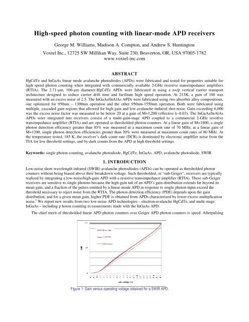
High-speed photon counting with linear-mode APD Receivers - Voxtel
High-speed photon counting with linear-mode APD Receivers - Voxtel
High-speed photon counting with linear-mode APD Receivers - Voxtel

You also want an ePaper? Increase the reach of your titles
YUMPU automatically turns print PDFs into web optimized ePapers that Google loves.
Figure 2: Excess noise data measured for two 2.7-µm-cutoff electronavalanche<strong>APD</strong>s measured under 1550-nm illumination at 77 K and 215 K.and the need to quench the <strong>APD</strong> below its breakdown voltage between detection events limits the maximum count rate (MCR) that can be achieved by a Geiger <strong>APD</strong>; typical quench times are well over1 µs. Sub-Geiger <strong>APD</strong>s are thought to be less susceptible to afterpulsing than Geiger <strong>APD</strong>s because less current flowsthrough the junction during detection events, and consequently there is a smaller change in trap occupancy; it is therelease of trapped carriers following a detection event that causes afterpulsing. The bias of a sub-Geiger <strong>APD</strong> <strong>photon</strong>counteris not gated during operation, and in free-run, the MCR is limited only by the <strong>APD</strong>’s impulse response duration– typically on the order of nanoseconds rather than microseconds. This <strong>speed</strong> advantage translates into much faster bitrates for single <strong>photon</strong> quantum information applications, and insensitivity to blinding by obscurants in single <strong>photon</strong>laser radar applications.Zhao et al. recently reported an InGaAs sub-Geiger single <strong>photon</strong> detector based upon a self-quenching gainsaturation mechanism, which operates at a gain of roughly 10 6 <strong>with</strong> a 30-ns single <strong>photon</strong> response. 2 However, the selfquenchingdevice’s 300-ns recovery time limits its MCR to rates similar to Geiger <strong>APD</strong> technology. The sub-GeigerInGaAs single <strong>photon</strong> detectors reported here are more directly comparable to those of Clark et al., which wereassembled from an InGaAs <strong>APD</strong> <strong>with</strong> a thin bulk InAlAs multiplier and a 580-MHz RTIA. 3 A maximum single <strong>photon</strong>detection rate of 14%, an associated dark count rate (DCR) of 850 kHz, and MCR of about 50 MHz were reported forthose receivers. At 70%, the single <strong>photon</strong> detection rate of the multi-stage receiver reported here is significantly higher,but the 55-MHz DCR is also higher, owing to the elevated amplifier noise level of the 2-GHz RTIA used in our receiver(250 nA RMS versus 45 nA RMS for the 580-MHz TIA).Back-illuminated, SWIR-cutoff HgCdTe <strong>APD</strong>s were designed for high <strong>speed</strong> operation using a vertical chargeFigure 3: Excess noise factor measurement for a 7-stage InGaAs<strong>APD</strong> measured at 295K.(wafer 14376)
transport architecture. The vertical charge transport <strong>APD</strong> architecture reduces the drift time for photocarriers created byabsorbed <strong>photon</strong>s, as compared to lateral-collection ‘loop hole’ HgCdTe, which have comparably larger photocarrierdrift times. As predicted, the SWIR <strong>APD</strong>s performance was characterized low excess noise and <strong>with</strong> maximum gains of100. At these gain levels, <strong>photon</strong> <strong>counting</strong> <strong>with</strong> commercially-available RTIAs is not possible.2. COMPARISON OF SWIR HGCDTE <strong>APD</strong>S TO MULTI-STAGE INGAAS <strong>APD</strong>SElectron-avalanche HgCdTe <strong>APD</strong>s are good candidates for thresholded <strong>linear</strong> <strong>photon</strong> <strong>counting</strong> because of their lowmultiplication noise and high gain. The impact ionization process in bulk HgCdTe is inherently low noise 4 , <strong>with</strong> anexcess noise factor close to unity at gains as high as M=1000 for mid-wave infrared (MWIR)-cutoff alloycompositions. 1,5,6,7 However, MWIR-cutoff HgCdTe requires cryogenic cooling to suppress thermal dark current, and istherefore not suitable for all applications. SWIR-cutoff HgCdTe <strong>APD</strong>s have also been reported in the literature, but <strong>with</strong>lower maximum gain and higher noise than the MWIR-cutoff devices. Beck et al. reported an excess noise factor of F~2at a gain of M=25 for 2.2-µm-cutoff HgCdTe <strong>APD</strong>s measured at 297 K 8 ; the same group reported maximum avalanchegains just over M=100 for 2.6-µm-cutoff devices at 198 K in a paper by Mitra et al. 9 Other recent results in the literatureare similar for SWIR-cutoff HgCdTe <strong>APD</strong>s. 10The lower gain observed for SWIR-cutoff HgCdTe <strong>APD</strong>s is qualitatively consistent <strong>with</strong> Beck’s empirical <strong>mode</strong>l,although the fit parameter (a) relating bandgap (E G ) to threshold voltage (Vth) is quantitatively different for SWIR-cutoffmaterial than for MWIR-cutoff alloys: 11 M(V)=1+2 [2(V-Vth)/Vth] ; Vth = a×E G (1)Gain rises more slowly <strong>with</strong> applied reverse bias (V) for HgCdTe alloys <strong>with</strong> wider bandgap (larger E G ), so a lower gainis achieved at the maximum reverse bias that the <strong>APD</strong> structure can tolerate.We report excess noise data on a new electron-avalanche HgCdTe <strong>APD</strong> fabricated from 2.7-µm-cutoff, liquid-phaseepitaxy(LPE)-grown material. Excess noise data from a 150-µm-square device and a 100-µm-diameter circular deviceare plotted in Figure 2. The <strong>APD</strong>s were tested at 77 K and 215 K under 1550-nm illumination. Our 215 K data closelymatches that published previously by Beck et al. for their 2.2-µm-cutoff device, which was measured at roomtemperature up to a gain of M=25. 8 It can be seen that at higher gains, the excess noise factor measured at 215 K liesslightly above the F=2 asymptote corresponding to purely single-carrier multiplication (k=0), and fits an effectiveimpact-ionization coefficient ratio of somewhat less than k=0.01, according to McIntyre’s formula: 122⎡ ⎛ M −1⎞⎤F ( M , k)= M ⎢1− (1 − k)⎜ ⎟ ⎥ . (2)⎢⎣⎝ M ⎠ ⎥⎦At 77 K, the measured excess noise falls below the F=2 asymptote, and the SWIR <strong>APD</strong>s behave more like the F~1MWIR electron-avalanche devices, <strong>with</strong> the likely added excess noise effects of phonon scattering increasing themeasured excess noise to F~1.5.<strong>High</strong>ly impact-ionization-engineered (I 2 E) InGaAs <strong>APD</strong>s are another candidate for thresholded <strong>linear</strong> <strong>photon</strong>Figure 4: Excess noise factor measurement 1t 295K of 10-stage InGaAs<strong>APD</strong>s Wafer 14148 from (13).
notably flatter for McIntyre-distributed <strong>APD</strong> noise (amplified dark current) than for Gaussian-distributed RTIA noise.Qualitative comparison of Figure 8 to DCR profiles measured for 5-, 8-, and 10-stage <strong>APD</strong> receivers operated at again of M=1200 (Figure 9) demonstrates that the 10-stage receiver’s DCR is dominated by false counts from theamplifier, rather than from the <strong>APD</strong> itself. To obtain a total gain of M=1200, <strong>APD</strong>s <strong>with</strong> fewer number of gain stages,require the gain from each multiplication state to be higher, in proportion to the power law. As the operating requiredfrom each <strong>APD</strong> multiplication stage increases, the dark counts the <strong>APD</strong> come to dominate the DCR. This is becauseincreasing the gain-per-stage requires a higher electric field, and tunnel leakage is an exponential function of electricfield strength in the junction.Figure 10 is a plot of PDE and DCR profiles for four <strong>photon</strong>-<strong>counting</strong> sub-Geiger receivers operated at an averagegain of M=1200. Similar results are obtained for all four devices.4. CONCLUSIONSExcess multiplication noise data for two low-noise SWIR <strong>APD</strong> technologies was compared. Multiplication noise inSWIR-cutoff HgCdTe <strong>APD</strong>s was found to be somewhat lower than in multi-stage InGaAs <strong>APD</strong>s, but the SWIR-cutoffHgCdTe devices demonstrated to date cannot operate at gains higher than about M=100. In contrast, 10-stage InGaAs<strong>APD</strong>s can operate at gains over M>1000 <strong>with</strong> low multiplication noise.The high gain and low noise of the multi-stage InGaAs <strong>APD</strong> makes it suitable for thresholded <strong>linear</strong>-<strong>mode</strong> <strong>photon</strong><strong>counting</strong>. Photon-<strong>counting</strong> receivers assembled from 10-stage InGaAs <strong>APD</strong>s have been demonstrated <strong>with</strong> PDE as highas 70% at an MCR of 25 MHz, but <strong>with</strong> a high DCR of approximately 100 MHz. The dependence of DCR on thresholdindicates that the majority of the false counts under these operating conditions originate in the RTIA rather than the <strong>APD</strong>itself.Future work will configure these multi-stage <strong>APD</strong>s <strong>with</strong> low noise capacitance transimedance amplifiers (CTIAs)<strong>with</strong> much lower noise, so that the DCR can significantly reduced. Further improvements in performance can beachieved by increasing the number of gain stages used in the multi-stage design, allowing the <strong>APD</strong> to be operated <strong>with</strong>lower noise at even higher gain, so that the count threshold may be set higher to reject more of the amplifier noise.ACKNOWLEDGEMENTSThe authors wish to acknowledge the support and encouragement of Allan Migdall who sponsored investigation of darkcounts in multi-stage InGaAs <strong>photon</strong> counters under contract NB200020-8-05349, and Xiaoli Sun who is sponsoringdevelopment of SWIR-cutoff HgCdTe <strong>APD</strong>s for <strong>photon</strong> <strong>counting</strong> under contract NNX08CA29C.Figure 10: PDE and DCR profiles of four different thresholded <strong>linear</strong> <strong>photon</strong>-counters assembledfrom 10-stage InGaAs <strong>APD</strong>s and 2-GHz RTIAs, operated at 180K and a gain of M=1200, <strong>with</strong>similar characteristics. Note that the DCR at the threshold level of 10 mV remains close to thatmeasured in the M=1800 case shown in Figure 7. At the threshold level of 15 mV, the DCD isreduced by a factor of 10X lower than the M=1880 data, showing that at low threshold levels, theGaussian shaped distribution from the RTIA dominates. At the higher threshold levels, dark countsfrom the <strong>APD</strong> dominate.
REFERENCES1. A. S. Huntington, M. A. Compton, and G. M. Williams, “Linear-<strong>mode</strong> single-<strong>photon</strong> <strong>APD</strong> detectors,” Proceedingsof SPIE, vol. 6771, 67710Q (2007).2. K. Zhao, A. Zhang, Y. Lo, and W. Farr, “InGaAs single <strong>photon</strong> avalanche detector <strong>with</strong> ultralow excess noise,”Applied Physics Letters, vol. 91, 081107 (2007).3. W. R. Clark, K. Vaccaro, and W. D. Waters, “InAlAs-InGaAs based avalanche photodiodes for next generation eyesafeoptical receivers,” Proceedings of SPIE, vol. 6796, 67962H (2007).4. F. Ma, X. Li, J. C. Campbell, J. D. Beck, C. Wan, and M. A. Kinch, “Monte Carlo simulations of Hg 0.7 Cd 0.3 Teavalanche photodiodes and resonance phenomenon in the multiplication noise,” Applied Physics Letters, vol. 83, no. 4,pp. 785-787 (2003).5. J. Beck, C. Wan, M. Kinch, J. Robinson, P. Mitra, R. Scritchfield, F. Ma, and J. Campbell, “The HgCdTe ElectronAvalanche Photodiode,” Infrared Detector Materials and Devices, Proceedings of SPIE, vol. 5564, pp. 44-53 (2004).6. M. A. Kinch, J. D. Beck, C.-F. Wan, F. Ma, and J. Campbell, “HgCdTe electron avalanche photodiodes,” Journal ofElectronic Materials, vol. 33, no. 6, pp. 630-639 (2004).7. R. S. Hall, N. T. Gordon, J. Giess, J. E. Hails, A. Graham, D. C. Herbert, D. J. Hall, P. Southern, J. W. Cairns, D. J.Lees, and T. Ashley, “Photomultiplication <strong>with</strong> low excess noise factor in MWIR to optical fiber compatiblewavelengths in cooled HgCdTe mesa diodes,” Infrared Technology and Applications XXXI, Proceedings of SPIE, vol.5783, pp. 412-423 (2005).8. J. Beck, C. Wan, M. Kinch, J. Robinson, P. Mitra, R. Scritchfield, F. Ma, and J. Campbell, “The HgCdTe ElectronAvalanche Photodiode,” Proceedings of SPIE, vol. 5564, 44 (2004).9. P. Mitra, J. D. Beck, M. R. Skokan, J. E. Robinson, J. Antoszewski, K. J. Winchester, A. J. Keating, T. Nguyen, K.K. M. B. D. Silva, C. A. Musca, J. M. Dell, and L. Faraone, “SWIR hyperspectral detection <strong>with</strong> integrated HgCdTedetector and tunable MEMS filter,” Proceedings of SPIE, vol. 6295, 62950G (2006).10. J. Rothman, G. Perrais, P. Ballet, L. Mollard, S. Gout, and J.-P. Chamonal, “Latest Developments of HgCdTe e-<strong>APD</strong>s at CEA LETI-Minatec,” Journal of Electronic Materials, vol. 37, no. 9, pp. 1303-1310 (2008).11. M. A. Kinch, J. D. Beck, C. –F. Wan, F. Ma, and J. Campbell, “HgCdTe electron avalanche photodiodes,” Journalof Electronics Materials, vol. 33, no. 6, (2004).12. R. J. McIntyre, “Multiplication noise in uniform avalanche photodiodes,” IEEE Transactions on Electron Devices,vol. ED-13, pp. 164-168 (1966).13. G. Williams, “GHz-rate single-<strong>photon</strong>-sensitive <strong>linear</strong>-<strong>mode</strong> <strong>APD</strong> receivers,” Proceedings of SPIE, vol. 7222,72221L (2009).14. C. Lenox, P. Yuan, H. Nie, O. Baklenov, C. Hansing, J. C. Campbell, A. L. Holmes, Jr., and B. G. Streetman, “Thinmultiplication region InAlAs homojunction avalanche photodiodes,” Applied Physics Letters, vol. 73, no. 6, pp. 783-784(1996).