GaAs-Wafer Dicing Using the Water jet Guided Laser - CS Mantech
GaAs-Wafer Dicing Using the Water jet Guided Laser - CS Mantech
GaAs-Wafer Dicing Using the Water jet Guided Laser - CS Mantech
- No tags were found...

Create successful ePaper yourself
Turn your PDF publications into a flip-book with our unique Google optimized e-Paper software.
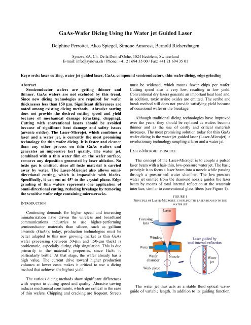
<strong>GaAs</strong>-<strong>Wafer</strong> <strong>Dicing</strong> <strong>Using</strong> <strong>the</strong> <strong>Water</strong> <strong>jet</strong> <strong>Guided</strong> <strong>Laser</strong>Delphine Perrottet, Akos Spiegel, Simone Amorosi, Bernold RicherzhagenSynova SA, Ch. De la Dent-d’Oche, 1024 Ecublens, SwitzerlandE-mail: info@synova.ch / Phone: +41 21 694 35 00 / Fax: +41 21 694 35 01Keywords: laser cutting, water <strong>jet</strong> guided laser, <strong>GaAs</strong>, compound semiconductors, thin wafer dicing, edge grindingAbstractSemiconductor wafers are getting thinner andthinner. <strong>GaAs</strong> wafers are not excluded by this trend.Since new dicing technologies are required for waferthicknesses less than 150 µm. Significant differences arenoted among existing dicing methods. Abrasive sawingdoes not provide <strong>the</strong> desired cutting speed and yieldbecause of mechanical damage (cracking, chipping).Cutting with conventional lasers should be avoidedbecause of significant heat damage and safety issues(arsenic oxides). The <strong>Laser</strong>-Micro<strong>jet</strong>, which combines alaser and a water <strong>jet</strong>, is currently <strong>the</strong> most promisingtechnology for thin wafer dicing. It is faster and cleanerthan any o<strong>the</strong>r process on thin <strong>GaAs</strong> wafers andgenerates an impressive kerf quality. The water <strong>jet</strong>,combined with a thin water film on <strong>the</strong> wafer surface,removes any deposition generated by laser ablation. Notoxic gas is emitted, since all toxic material is carriedaway by water. The <strong>Laser</strong>-Micro<strong>jet</strong> also allows omnidirectionalcutting, which is impossible with blades.Specifically, it can cut at 45° to <strong>the</strong> crystal plane. Edgegrinding of thin wafers represents one application ofomni-directional cutting, reducing breakage by removing<strong>the</strong> sensitive wafer edge containing micro-cracks.INTRODUCTIONmust be widened, which means fewer chips per wafer.Cutting speed also is very low, resulting in low yield.Conventional dry lasers generate an important heat load and,in addition, toxic arsine oxides are emitted. The scribe andbreak method still does not provide satisfying yield becauseof occasional wafer or die breakage.Although traditional dicing technologies have improvedover <strong>the</strong> years, <strong>the</strong>y should be replaced as wafers becomethinner and as <strong>the</strong> use of costly and critical materialsincreases. The most promising solution today for thin <strong>GaAs</strong>wafer dicing is <strong>the</strong> water <strong>jet</strong> guided laser (<strong>Laser</strong>-Micro<strong>jet</strong>), arevolutionary technology coupling a laser and a water <strong>jet</strong>.LASER-MICROJET PRINCIPLEThe concept of <strong>the</strong> <strong>Laser</strong>-Micro<strong>jet</strong> is to couple a pulsedlaser beam with a hair-thin, low-pressure water <strong>jet</strong>. The basicprinciple is to focus a laser beam into a nozzle while passingthrough a pressurized water chamber. The low-pressurewater <strong>jet</strong> emitted from <strong>the</strong> diamond nozzle guides <strong>the</strong> laserbeam by means of total internal reflection at <strong>the</strong> water/airinterface, similar to conventional glass fibers (see Figure 1).FIGURE 1PRINCIPLE OF LASER-MICROJET: COUPLING THE LASER BEAM INTO THEWATER JETContinuing demands for higher speed and increasingminiaturization have driven <strong>the</strong> wireless and broadbandcommunications industries to use higher-performingsemiconductor materials than silicon, such as galliumarsenide (<strong>GaAs</strong>); today, production technologies must bebetter adapted to this new growing market as thin <strong>GaAs</strong>wafer processing (between 50-µm and 150-µm thick) isproblematic, especially during chip singulation. This is dueprimarily to <strong>the</strong> material’s properties, since <strong>GaAs</strong> isparticularly brittle. At that stage, <strong>the</strong> wafer already has ahigh value. The current drive toward higher productionvolumes at lower costs makes it critical to use a dicingmethod that achieves <strong>the</strong> highest yield.The various dicing methods show significant differenceswith respect to cutting speed and quality. Abrasive sawinginduces mechanical constraints, which are critical in <strong>the</strong> caseof thin wafers. Chipping and cracking are frequent. StreetsThe water <strong>jet</strong> thus acts as a stable fluid optical waveguideof variable length. In addition to its guiding function,
it has two o<strong>the</strong>r primary effects. First, it cools <strong>the</strong> materialbetween <strong>the</strong> laser pulses so <strong>the</strong> heat-affected zone isnegligible. Second, thanks to its high momentum, it removesmost of <strong>the</strong> molten material generated by laser ablation.Additionally, a thin water film on <strong>the</strong> material preventsparticles from adhering to <strong>the</strong> wafer surface. The <strong>Laser</strong>-Micro<strong>jet</strong> is <strong>the</strong>refore significantly different from <strong>the</strong> drylaser, which pose <strong>the</strong> major disadvantages of contaminationand heat damage.FIGURE 228-UM WIDE THROUGH-CUT IN A 100-UM THICK GAAS WAFER: A CHIPPING-FREE CUTThe <strong>Laser</strong>-Micro<strong>jet</strong> also offers advantages over abrasivesawing. It is a faster process; depending on <strong>the</strong> material, upto 10 times faster. Fur<strong>the</strong>rmore, <strong>the</strong> mechanical force appliedby <strong>the</strong> water <strong>jet</strong> is negligible (less than 0.1 N), in contrary tosawing. This force is also much lower than <strong>the</strong> force appliedby <strong>the</strong> assist gas in conventional dry laser cutting.The <strong>Laser</strong>-Micro<strong>jet</strong> is <strong>the</strong>refore an efficient technologyfor semiconductor processing, including III-V compositematerials as well as silicon. Its main applications in this fieldare thin wafer dicing (through-cutting), scribing and edgegrinding. Recent developments on nozzles have enabledstable cutting with a micro-<strong>jet</strong> as thin as 25 µm.The main advantages of <strong>GaAs</strong> cutting with <strong>the</strong> <strong>Laser</strong>-Micro<strong>jet</strong> are: high speed; no mechanical forces; no crackingor chipping; low kerf width; no contamination; no toxicproducts; and possibility to cut through back metal. Inaddition, it can cut at 45° to <strong>the</strong> standard crystal orientation.Omni-directional cutting offers <strong>the</strong> desirable application ofedge grinding of thin wafers. Thus, by removing <strong>the</strong> edge ofwafers, micro-cracks generated by back grinding areeliminated, <strong>the</strong>reby reducing wafer breakage.GAAS WAFER CUTTING AND LASER-MICROJETUsually, <strong>the</strong> <strong>Laser</strong>-Micro<strong>jet</strong> is applied for throughcutting.Figure 2 shows <strong>the</strong> typical quality obtained with <strong>the</strong>LMJ process on <strong>GaAs</strong> wafer. There is no chipping due tomechanical stress and very low contamination. For this 100-µm thick <strong>GaAs</strong> wafer, a fiber laser (wavelength 1064 nm,average power 100 W) has been coupled into a thin water <strong>jet</strong>(diameter 27 µm). These parameters were chosen to obtainhigh cut quality at high speed. Speeds up to 80 mm/s havebeen achieved.1) Particle contamination: <strong>the</strong> <strong>Laser</strong>-Micro<strong>jet</strong> produceslittle contamination, since <strong>the</strong> water <strong>jet</strong> used to guide <strong>the</strong>laser beam onto <strong>the</strong> work piece also efficiently removesmost of <strong>the</strong> molten material. An additional device hasrecently been developed to reduce particle contaminationlevel even fur<strong>the</strong>r. During cutting, a continuous water layerof controlled thickness covers <strong>the</strong> wafer, preventing <strong>the</strong>particles from attaching to <strong>the</strong> material surface. Removing<strong>the</strong> water layer containing suspended particles after cuttingguarantees a clean wafer. The result is especially impressivecompared to conventional laser cutting. Figure 3 provides anexample of <strong>the</strong> cut quality. For this 100-µm thick wafer, aQ-switched Nd:YAG laser (wavelength 1064 nm, averagepower 50 W) has been coupled into a water <strong>jet</strong> of 25 µmdiameter. Even at high speed (60 mm/s), <strong>the</strong> cut quality isexcellent.FIGURE 326-UM WIDE THROUGH-CUT IN A 100-UM THICK GAAS WAFER: A CHIPPING-FREE CUT AT 60 MM/S2) Toxicity of <strong>GaAs</strong> ablation: safety issues are paramountduring cutting since compound <strong>GaAs</strong> contains 51.8%wtarsenic. Tests performed with <strong>the</strong> <strong>Laser</strong>-Micro<strong>jet</strong> (see Table
1) showed that no arsine gas is detected in <strong>the</strong> air whilecutting <strong>GaAs</strong>. This represents a significant improvementcompared to conventional laser cutting [1]. All arsenic isconcentrated in <strong>the</strong> wastewater, which should <strong>the</strong>refore beappropriately filtered or recycled. Thus, <strong>Laser</strong>-Micro<strong>jet</strong>dicing of <strong>GaAs</strong> does not require any additional securitysystems comparable to sawing.distance of 1 mm of <strong>the</strong> edge and <strong>the</strong> grooving depth was 80µm. The resulting process speed was 50 mm/s.FIGURE 5EDGE GRINDING OF A WAFER, 1 MM FROM THE EDGE AND 80-UM DEEPTABLE 1RESULTS FROM THE GAAS TRIAL RUN: ARSENIC CONCENTRATIONArsine gas [ppm]Not detectedConcentration of As in air [µg/m3]Concentration of As in water [µg/L]Wipe sample results [µg/cm2]130 (in cutting chamber)4 (outside machine)6270030 (in cutting chamber)0.062 (next to machine)3) Omni-directional cutting: unlike saws, <strong>the</strong> <strong>Laser</strong>-Micro<strong>jet</strong> can cut in any direction. Specifically, it is possibleto cut at 45° to <strong>the</strong> main crystal plane. Free-shape cutting –also known as free form or arbitrary cutting – of thin wafershas become increasingly important for various applicationsin microelectronics, in which arbitrary-shaped chips areused. Figure 4 shows a 178-µm thick <strong>GaAs</strong> wafer cut with<strong>the</strong> <strong>Laser</strong>-Micro<strong>jet</strong> at a speed of 15 mm/s.FIGURE 4FREE-SHAPE CUTTING IN A 178-UM THICK GAAS WAFER; KERF WIDTH 50UM; CUTTING SPEED 15 MM/SCONCLUSIONSThe <strong>Laser</strong>-Micro<strong>jet</strong> is currently <strong>the</strong> most promisingtechnology for thin wafer dicing, especially when thicknessis less than 150 µm or when delicate materials are used. Ithas proven better able to dice thin <strong>GaAs</strong> wafers than anyo<strong>the</strong>r dicing methods, such as sawing, conventional dry laserand scribe and break techniques. The heat-affected zone isnegligible thanks to <strong>the</strong> water <strong>jet</strong> that cools <strong>the</strong> cut edgesduring laser ablation. Molten material is efficiently removedand does not adhere. Cutting speeds are much higher thanwith sawing (up to 80 mm/s in 100-µm thick <strong>GaAs</strong>), whileachieving an excellent cut quality. Currently, kerf widths asthin as 25 µm can be achieved; new nozzles being tested in<strong>the</strong> laboratory will produce ultra-thin <strong>jet</strong>s of only 17-µmdiameter. Regarding safety, only conventional proceduresare required (wastewater treatment). Finally, omnidirectionalcutting allows wafer edge grinding, reducingwafer-breakage.ACKNOWLEDGEMENTSThe authors would like to thank <strong>the</strong> clients who provided<strong>the</strong> samples and additional information.4) Edge grinding of thin wafers: edge grinding isintended to reduce thin wafer breakage. It consists of a cut ora groove around <strong>the</strong> wafer to remove micro-cracksaccumulated in <strong>the</strong> edge. This operation can be performedei<strong>the</strong>r before or after back grinding, depending on <strong>the</strong>application. Figure 5 shows a wafer grooved using a diodepumpedfiber laser (wavelength 1064 nm, average power 80W) and a 75-µm nozzle. The wafer has been grooved at aREFERENCES[1] N. Dushkina, <strong>Dicing</strong> <strong>GaAs</strong> wafers, Industrial <strong>Laser</strong> Solutions, June2003.[2] O. Sibailly, F. Wagner, B. Richerzhagen, <strong>Laser</strong>-Edge Grinding of Thin<strong>Wafer</strong>s with <strong>the</strong> <strong>Water</strong>-Jet-<strong>Guided</strong> <strong>Laser</strong>, Future Fab International 16,February 2004.ACRONYMSLMJ: <strong>Laser</strong>-Micro<strong>jet</strong>