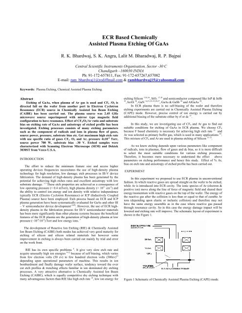
ECR Based Chemically Assisted Plasma Etching Of ... - CS Mantech
ECR Based Chemically Assisted Plasma Etching Of ... - CS Mantech
ECR Based Chemically Assisted Plasma Etching Of ... - CS Mantech

You also want an ePaper? Increase the reach of your titles
YUMPU automatically turns print PDFs into web optimized ePapers that Google loves.
In <strong>ECR</strong> illuminating a magnetized region with high-power microwaveradiation created plasma. At a magnetic field of about 875 Gauss, theelectron Larmor frequency is equal to the microwave frequency of 2.45 GHz(it is the microwave oven frequency). At low enough pressures, electronsgain energy on each circuit around the field lines; this field allows bothconfinement and efficient electron heating. <strong>ECR</strong> sources can achievedensities around 10 12 /cm 3 ions at pressures of a few mTorr (this is severalpercent ionization). The <strong>ECR</strong> has very low energy plasma potential. In orderto achieve significant sputtering rates at the wafer, it is necessary to apply abias, and has been carried out by dc bias.The vacuum system includes Varian mechanical pump, model SD-300capacity 300 liters per minute and Varian cryopump model Cryostack-8capacity 1500 lts/sec. The pressure of the gas is measured with two gauges,ionization gauge for measuring pressure in the range of 10 -3 Torr and below,capacitance diaphragm gauge from Vacuum General model CMH-01 forpressure range of 10 -4 to 1Torr. Alphagaz mass flow controller controlled thegas flow. The microwave power was generated by a continuously variablemicrowave power supply from M/s ASTeX, USA (50 to 1000 watts atfrequency 2.45 GHz). Microwave in TM 01 mode was launched in the sourceregion through quartz window. A three-stub tuner is used to tune thereflected power to the minimum value. A set of two-solenoid coils surround'sthe cavity, where the plasma is produced. Each coil is powered by two EMSpower supply model EMS 20-125-2D and EMS 27-185-2D. The entrancecoil is powered by 180 Amp, 27 Volts supply while exit coil is powered by120 Amp, 20V. The independent powered coils provide a static magneticfield of the order of 1.25 KGauss by entrance coil and 0.87 KGauss by exitcoil. The two together create the resonance condition for efficient microwaveabsorption in the source 13 .In the <strong>ECR</strong> machine, the plasma excited by a microwave field in thepresence of a dc magnetic field of the correct magnitude to cause theelectrons to gyrate at the microwave field frequencies thus increasing theprobability of ionization. The potential advantage of the <strong>ECR</strong> in thisseparation of the fields, which is first create the plasma and then impartenergy to the ions. In general, two main advantage of dry etching are (i) theuse of highly directed ions results in a profile of the etched material, whichcan be anisotropic, (i.e. vertical walls can be formed) and (ii) it is possible toobtain better uniformity over the wafer. This investigation on the use of CF 4 ,O 2 and Ar as posses gases, where AR was used aid in an isotropic and O 2 inreduction of residual surface polymers.RESULT AND DISCUSSIONThe etch rate of GaAs, at a pressure of 0.4 mTorr, 700 W input powerand negative 30V bias as a function of flow of CF 4 + O 2 gases at differentArgon (Ar) flows (20, 10 & 0 SCCM). in figure. 2 It has been observed thatin last two cases, etch rate increases till the flow of CF 4 equals that of Arflow and there after etch rate decreases. Maximum etch rate achieved are 190A 0 /min, 130 A 0 /min were at 10, 20, SCCM of Ar flows respectively. With noArgon flow in cavity, the etch rate increase from 70 A 0 /min to 107 A 0 /minand then saturate but there is no peaking in etch rate.20 SCCM of Ar is made to flow into <strong>ECR</strong> cavity while CF 4 gas isvaried from 0 - 50 SCCM in case 1. Ar gas under goes followingtransformation in <strong>ECR</strong> cavity.Ar + e - Ar + + 2e - (1)Electrons and Argon ions move down the cavity towards the waferswhere CF 4 molecules sprayed on the wafer. The ions are further acceleratednear the wafer by the negative bias, these Ar ions and secondary electronsthen ionize some of the CF 4 molecules and produces free atoms and CF 4radicals. As the CF 4 increased further, the probability of secondary electronsand ions striking CF 4 molecules increases and increasing free F atoms. Thisincreases F/Argon atoms ratio striking the silicon wafer and this leads toincrease in etch rate 32 . These trends continue, till the volume of CF 4 equalsthat of constant flow of Argon (i.e. 20 SCCM) in the cavity. This trend isreversed when the flow of CF 4 is increased beyond 20 SCCM and etch rateof GaAs start decreasing. These characteristics may be due to the facts thatthe probability of getting reaction on the GaAs surface producing nonvolatize product increases beyond 50 % of CF 4 flow and leads to decrease inetching rate 35 . Abundance of CF 4 beyond 50% over silicon wafer, decreasesthe ratio of active species (fluorine atoms) to neutrals 36,37 reaching the waferand thereby decreasing the etch rate. Another reason may be that beyond 50% flow of CF 4 (i.e. > 20 SCCM) the probability of getting CF 4 ionizeddecreases even for best efficiency of ionization in <strong>ECR</strong> cavity and therebydecreasing active species to neutral ratio. This lead to increase in amount ofneutrals or molecules, which are not useful in etching. These neutrals andmolecules get adsorbed on the silicon surface and inhibit etching anddecrease etching rate 36, 37 . Maximum etch rate (190 A 0 /min) is achieved for10 SCCM of Argon in cavity with 10 SCCM of CF 4 on silicon wafer. Thismay be due to decrease in active fluorine to neutral ratio over the siliconwafer & will result in decrease in etching rates. Efforts were also made foretching study at 5 SCCM of Ar flow in the <strong>ECR</strong> cavity and 5 SCCM of CF 4flow on the wafer surface. It was noticed that the reflected power in this casewas more than 50% and was not tunable with three stub tuner and thereforedetail studies of etching at these flows was not carried out.It has been observed that, where no Ar is given in the <strong>ECR</strong> cavity and CF 4neutral are spread on the wafer, the etching characteristics are totallydifferent from above observation and are of the order of 5-10 A 0 /min only 38 .In our experiment with no argon in the cavity we observed that the curves donot pass through maxima. Etch rate increases from 70 A 0 /min to 107 A 0 /minwith increase in CF 4 & then saturate. This may be due to the absence of ions& secondary electron of argon from the <strong>ECR</strong> cavity. However etching of Siis not because of neutrals of CF 4 which is of the order of 5-10 A 0 /min, butbecause of diffusion of CF 4 into <strong>ECR</strong> cavity and then providing activesspecies for etching, which are then transported back to wafer surface.Marginal increase in etching may be due initial increase of active specieswith increase of CF 4 flow.220200180CF 4/O 2& Ar 10 SCCM eachCF 4/O 2& Ar 20 SCCM eachCF 4/O 2& Ar nil SCCM each160Etch rate (A 0 /min)220200180160140120100Ar NilAr 10 SCCMAr 20 SCCMEtch rate (A 0 /min)14012010080604080206010 20 30 40 50Flow of CF 4-50 -40 -30 -20 -10 0Bias with negative voltageFigure 2 Plot between Etch rate (A 0 /min) and CF 4 /O 2 at constant Ar 0,10,20SCCM.Figure 3 Variation of Etch rate (A 0 /min) with bias in CAPE mode atconstant flow of CF 4 / O 2 and Ar at 10,20, & nil SCCM each.
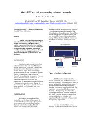
The <strong>ECR</strong> has low plasma potential. In order to control bias, it isnecessary to apply separate power supply. Figure 3 represent etch rate versusbias characteristics at 0.4 mTorr pressure, 700 watts input power. Where DCpower supply has been used to vary the voltage from 0 to – 50 volts. It hasbeen observed that the Etch rate increase from 0 to - 30 volts (102 A 0 /min to210 A 0 /min) and then beyond - 30 volts it decreases (210 A 0 /min to 40A 0 /min). The increase in etch rate can be attributed the fact that Ar ions andelectrons from the cavity has a very small energy, as these approaches thewafer, the positive ions encounter negative electric field, & gets acceleratedand its energy is increased. This enhanced energy of Ar ions leads to increasein ionization of CF 4 neutrals which is between 5-10 % 39 and therebyproducing more active etching radicals (CF 3 , CF 2 and C). This leads to theincrease etch rate. The decrease in etch rate beyond –30 volts bias, may bebecause of a few reasons. One of them is formation of passivation layernCF 2(s) on Si wafer; beyond certain % of CF 4 , which resist to etching on thewafer 40 . Other reason for decrease in etching rate may be that because of DCbias; there may be charge accumulation on the wafer, which do not getneutralized as in the case of RF. The charge accumulation can scatter activespecies thereby leading to reduction in etch rate on the Si wafer. Anotherreason may be due to sputter redeposition or other reactant etch species,given the inherent competition in etch process between sputter removal andredeposition of reactants.Figure 4 is the scanning electron micrographs of the trench for study ofanisotropy, which is defined as 41 .A = 1- V h /V vWhere V h is the horizontal etch rate and V v is the vertical etch rate.These micrograph of GaAs is taken at 0.4 mTorr pressure, 700 watts inputpower and negative 30 volts bias with CF 4 & Ar flow 10 SCCM each. It hasbeen observed that the anisotropy in figure 4 is 0.8. The reason for goodanisotropy at low CF 4 /Ar flow may be attributed to the many facts. First thepresence of energetic electron along with availability of CF 4 molecule inabundance leads to following reaction.CF 4 + e - → CFx + + CFxo + F o + e - (2)CFxo → nCF 2 (ads) → nCF 2 (s) (3)nCF 2(s) + F o → ion energy →CF x(ads) →CF x(g) (4)This lead to formation of passivating layer on all the surface of thetrench as indicated in equation (4). With higher CF 4 flow, the probability offormation of passivation layer may be earlier than lower CF 4 flow because ofabundance of CF 4 molecules. The passivating layer nCF 2 (s) inhibit furtheretching of the Si from the sidewall as well as trench surface (2) and therebyleading to decrease in etching rate and anisotropy. This process can bereversed by the application of energetic ions on the passivating layer nCF 2 (s)indicated in equation (4). However in case of DC bias, because of chargeaccumulation and surface sparking, this process could not be carried out. SoJudicious chemistry selection is very difficult to finely control this balancebetween etching and the deposition.ConclusionIn <strong>ECR</strong> plasma source with a mirror type magnetic field configurationsystem, anisotropy & etch rate of GaAs in CAPE mode was evaluated with% of CF 4 , flow of gases, and bias. Following conclusion from theinvestigation has been drawn.(a)(b)(c)In CAPE mode with CF 4 /Ar plasma, etch rate increase withincrease CF 4 for GaAs and trend was reversed after increaseCF 4 greater than 50%.The etch rate of GaAs increased (102 A 0 /min to 210 A 0 /min)with negative bias it was maximum around – 30 volts.The formation of passivating layer nCF 2 (s) , which inhibitfurther etching, is more beyond 50% flow of reactive gases.This study demonstrates the viability of <strong>ECR</strong> high-density plasma forlow damage and high etching in the fabrication of III-V devices. This is agood application for this technology , which allows for the development oflow cost, high throughput production process for devices requiring submicron critical dimension.AcknowledgementsWe are grateful to Prof. Nirmal Singh for scientific discussion, whichis helpful to us for this paper. We also thanks to trainees Mr. Vikesh Raj andMr. Pankaj Kumar for data collection.References[1] E.L. Hu, C-H and D.L. Green, J. Vac. Sci. Technol., B 14, 3632(1996).[2] J. Wada, Y. Matsukura, T. Ogihara and O. Ueda, J. Appl. Phys.,82, 617 (1997).[3] J.W. Lee, S.J. Pearton, F. Ren, R.F. Kopf, J.M. Kuo, R.J.Shul, C.Constantine and D. Johnson, J. Electrochem. Soc., 145, 4036 (1998).[4]C. Constantine et. al., Mat. Es. Soc. SYMP. Proc., 421, 431 (1996).[5] F. Ren, W.S. Hobson, J.R. Lothian, J. Lopata, S.J. Pearton, J.A.Caballero and M.W. Cole, J. Electrochem. Soc., 143, 3394 (1996).[6] D. Bose, T.R. Govindan and Meyyappan, J. Electrochem. Soc.,146, 2705 (1999).[7] S. K. Angra, P. Kumar, P. C. Banerjie and R. P. Bajpai J. Thinsolid films 304, 294 (1997).Figure 4 Micrograph of etching profile in <strong>Chemically</strong> <strong>Assisted</strong> <strong>Plasma</strong><strong>Etching</strong> (CAPE) mode of GaAs are taken at 0.4 mTorr pressure, 600 wattsinput power and negative 30 volts bias with CF 4 /O 2 & Ar flow 10 SCCMeach.[8] H. Jansan, H. Gardeniers, M. D. Boer, M. Elwenspoek and J.Fluitman J. Micromech. & Microeng. (6) 14 (1996).[9] I. Adesida, A. Mahajan, E. Andideh, M. A. Khan, D. T. Olsen andJ. N. Kuznia, Appl. Phys. Lett. 63, 2777(1993).[10] M. E. Lin, Z. Fan, Z. Ma, L. H. Allen and H. Morkoc, Appl. Phys.Lett. 64,887 (1994).
[11] A. T. Ping, I. Adesida, M. A. Khan, and J. N. Kuznia, Electr. Lett.30, 1895 (1994).[12] S. J. Pearton, C. B. Vartuli, R. J. Shul and J. C. Zolper Mat. Sci.Eng. B31,309 (1995).[13] S. K. Angra, P. Kumar, and R. P. Bajpai, Indian J. Engineeringand Material Science (8), 205 (2001).[14] D. Peyrade, Y. Chen, L. M. Ferlazzo, A. Lebib, N. Grandjean, D.Coquillat, R. Legros and J. P. Lascaray Microelectronics Engineering57, 843 (2001).[15] J. Bhardwaj, H. Ashraf, A. McQuarrie Symposium onMicrostructure and Microfabricated System at the annual meeting ofthe Electrochemical Society, Quebee, Canada, May 4-9, 1997.[16] M. Loncar, D. Nedeljkovic, T. Doll, J. Vuckovic, A. Scherer andT. P. Pearsall Appl. Phys. Lett. 77(13) 1937 (2000).[17] B. O. Cho, S. W. Hwang, J. H. Ryu and S. H. Moon Review ofScientific Instruments 70 (5) 2458(1999).[18] C. J. Mogab, A. C. Adams and D. L. Flamm J. Appl. Phys. 49 (7)3796 (1978).[19] L. M. Bharadwaj, P. Bonhomme, J. Faure and R. P. Bajpai J.Vac. Sci. Technol. B 9(3) 1440 (1991).[20] C. Santori, D. Fattal, J.V. Kovi , G. S. Solomon and Y.Yamamoto, Nature 419, 594 (2002).[21] D. Peyrade, Y. Chen, L. M. Ferlazzo, A. Lebib, N. Grandjean, D.Coquillat, R. Legros and J. P. Lascaray Microelectronics Engineering57, 843 (2001).[22] C. Youtsey, A. T. Ping, G. Bulman and I. Adesida 58 th ElectronicMaterial Conference, Santa Barbara, California, June 26-28, 1996.[32] M. Matsui, F. Uchida, M. kojima, T. Tokunaga, K. Yamazaki Jpn.J. Appl. Phys. Part 1, 37, 2330 (1998); T. Nakano and S. Samukawa J.Vac. Sci. Technol. A 17, 686 (1999); 17, 500 (1999).[33] D. C. Marra and E. S. Aydil, J. Vac. Sci. Technol. A 15, 2508(1997).[34] K. E. Davis and C. M. Horwitz, J. Vac. Sci. Technol. A 7, 2705(1989).[35] F. Greer, K. Kurihara, J. W. Coburn rihara, J. W. Coburn and D.B. Graves Deptt. of Chemical Engg. University of California, Ca 94720Final report 1997-98 for micro project 97-054.[36] The Science and Engineering of Microelectronic Manufactureedited by S. A. Campbell Oxford University Press 2001.[37] <strong>Plasma</strong> <strong>Etching</strong> in Semiconductor Fabrication, edited by R.Morgan, ElsevierPress, NY, 1985.[38] <strong>Plasma</strong> <strong>Etching</strong> and Introduction, edited by D. Manos, D. Flamm,Academic Press, Inc., NY, 1989.[39] ULSI Technology International Editions 1996 Editor, C. Y. Chang& S. M. Sze Publisher, McGraw Hill.[40] B. H. Tseng PPT presentation at July 31, 2003 at National SunYat-Sen University.[41] G. S. Oehrlein, P. J. Matsuo, M. F. Doemling, N. R. Rueger, B. E.E. Kastenmeier, M. Schaepkens, T. Standaert and J. J. Beulens, <strong>Plasma</strong>Sources Sci. Technol. 5, 193 (1996).ACRONYMS<strong>ECR</strong>: Electron Cyclotron Resonance[23] I. Adesida, A. T. Ping, C. Youtsey, T. Dow, M. Asif Khan, D. T.Olson and J. N. Kuznia Appl. Phys. Lett. 65(7) 889 (1994).[24] A. T. Ping, C. Youtsey, I. Adesida, M. Asif Khan and J. N. KuzniaJ. Electron Mater, 24, (1995) 229.[25] W. –J. Lee, H. –S. Kim, G. –Y. Yeom, J. –W. Lee and Tae-II KimJ. Vac. Sci. Technol. A 17, 1230 (1999).[26] M. Scherer, V. Schwegler, M. Seyboth, F. Eberhard, C. Kirchner,M. Kamp, G. Ulu, M. S. Unlu, R. Gruhler and O. Hollricher J. CrystalGrowth 230, 554 (2001).[27] G. –Y. Yeom, , H. –S. Kim, S. K. Kwan, J. –W. Lee, Tae-II Kim,Y. –J. Lee, M. –C. Yoo Symposium Gallium Nitride and RelatedMaterials, April 1 - 4, 1997.[28] J. –W. Lee, M. –C. Yoo, Tae-II Kim, Symposium Gallium Nitrideand Related Materials, April 1 - 4, 1997.[29] L. M. Bharadwaj, P. Bonhomme, J. Faure, G. Balossier and R. P.Bajpai SPIE Proceeding 1593, 186 (1992).[30] S. –L. Wu, L. Wang, R. C. Tiberio and S. T. Ho SPIE Proceeding355 1, 59 (1998).[31] K. Hioki and H. hirata , J. Vac. Sci. Technol. A 18 (3) 864 (2000).