Development of L-band 28V Operation GaAs FET and ... - CS Mantech
Development of L-band 28V Operation GaAs FET and ... - CS Mantech
Development of L-band 28V Operation GaAs FET and ... - CS Mantech

Create successful ePaper yourself
Turn your PDF publications into a flip-book with our unique Google optimized e-Paper software.
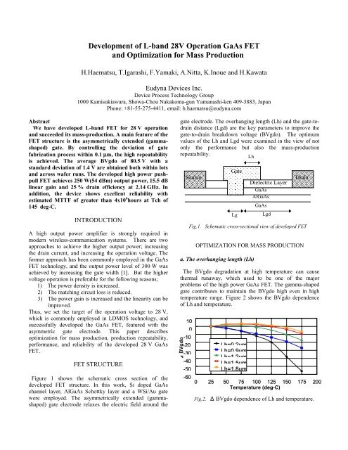
<strong>Development</strong> <strong>of</strong> L-<strong>b<strong>and</strong></strong> <strong>28V</strong> <strong>Operation</strong> <strong>GaAs</strong> <strong>FET</strong><strong>and</strong> Optimization for Mass ProductionH.Haematsu, T.Igarashi, F.Yamaki, A.Nitta, K.Inoue <strong>and</strong> H.KawataEudyna Devices Inc.Device Process Technology Group1000 Kamisukiawara, Showa-Chou Nakakoma-gun Yamanashi-ken 409-3883, JapanPhone: +81-55-275-4411, email: h.haematsu@eudyna.comAbstractWe have developed L-<strong>b<strong>and</strong></strong> <strong>FET</strong> for 28 V operation<strong>and</strong> succeeded its mass-production. A main feature <strong>of</strong> the<strong>FET</strong> structure is the asymmetrically extended (gammashaped)gate. By controlling the deviation <strong>of</strong> gatefabrication process within 0.1 µm, the high repeatabilityis achieved. The average BVgdo <strong>of</strong> 80.5 V with ast<strong>and</strong>ard deviation <strong>of</strong> 1.4 V are obtained both within lots<strong>and</strong> across wafer runs. The developed high power pushpull<strong>FET</strong> achieves 250 W(54 dBm) output power, 15.5 dBlinear gain <strong>and</strong> 25 % drain efficiency at 2.14 GHz. Inaddition, the device shows excellent reliability withestimated MTTF <strong>of</strong> greater than 4x10 6 hours at Tch <strong>of</strong>145 deg-C.INTRODUCTIONA high output power amplifier is strongly required inmodern wireless-communication systems. There are twoapproaches to achieve the higher output power; increasingthe drain current, <strong>and</strong> increasing the operation voltage. Theformer approach has been commonly employed in the <strong>GaAs</strong><strong>FET</strong> technology, <strong>and</strong> the output power level <strong>of</strong> 300 W wasachieved by increasing the gate width [1]. But the highervoltage operation is preferable for the following reasons;1) The power density is increased.2) The matching circuit loss is reduced.3) The power gain is increased <strong>and</strong> the linearity can beimproved.Thus, we set the target <strong>of</strong> the operation voltage to 28 V,which is commonly employed in LDMOS technology, <strong>and</strong>successfully developed the <strong>GaAs</strong> <strong>FET</strong>, featured with theasymmetric gate electrode. This paper describesoptimization for mass production, production repeatability,performance, <strong>and</strong> reliability <strong>of</strong> the developed 28 V <strong>GaAs</strong><strong>FET</strong>.<strong>FET</strong> STRUCTUREFigure 1 shows the schematic cross section <strong>of</strong> thedeveloped <strong>FET</strong> structure. In this work, Si doped <strong>GaAs</strong>channel layer, Al<strong>GaAs</strong> Schottky layer <strong>and</strong> a WSi/Au gatewere employed. The asymmetrically extended (gammashaped)gate electrode relaxes the electric field around thegate electrode. The overhanging length (Lh) <strong>and</strong> the gate-todraindistance (Lgd) are the key parameters to improve thegate-to-drain breakdown voltage (BVgdo). The optimumvalues <strong>of</strong> the Lh <strong>and</strong> Lgd were examined in the view <strong>of</strong> notonly the performance but also the mass-productionrepeatability.LhSourceGateLgOPTIMIZATION FOR MASS PRODUCTIONa. The overhanging length (Lh)Dielectric Layer<strong>GaAs</strong>Al<strong>GaAs</strong><strong>GaAs</strong>LgdDrainFig.1. Schematic cross-sectional view <strong>of</strong> developed <strong>FET</strong>The BVgdo degradation at high temperature can causethermal runaway, which used to be one <strong>of</strong> the majorproblems <strong>of</strong> the high power <strong>GaAs</strong> <strong>FET</strong>. The gamma-shapedgate contributes to maintain the BVgdo high even in hightemperature range. Figure 2 shows the BVgdo dependence<strong>of</strong> Lh <strong>and</strong> temperature.⊿BVgdo100-10-20-30-40-50-60Lh=0 2umLh=0 9umLh=1 2umLh=1 5umLh=1.8um0 25 50 75 100 125 150 175 200Temperature (deg-C)Fig.2. Δ BVgdo dependence <strong>of</strong> Lh <strong>and</strong> temperature.
To keep the adequate BVgdo level even at 175 deg-C, whichis our targeted maximum channel temperature, the Lh isrequired to set longer than 1.4 µm. On the other h<strong>and</strong>, thegate-drain feedback capacitance (Cgd) is in proportion to theLh, <strong>and</strong> which causes gain reduction. Figure 3 shows the∆Gsmax dependence <strong>of</strong> Lh. The degradation-rate <strong>of</strong> Gsmaxis estimated 0.13 dB/µm around Lh=1.5 µm.∆Gsmax (dB)0.60.40.20-0.2-0.4-0.6-0.8The actual Lh is determined by not only designed lengthbut also the alignment accuracy <strong>of</strong> the buried gatefabrication process <strong>and</strong> the over gate fabrication process.Therefore, we control this alignment deviation within0.1 µm <strong>and</strong> set the Lh to 1.5 µm, which ensures that Lh islonger than 1.4um even in the lower limit. In addition, thegain deviation, generated by this miss alignment, is less than0.2 dB.The rate is estimated 12 V/µm. The deviation <strong>of</strong> the Lgd isoriginated from the alignment <strong>of</strong> the ohmic metalizationprocess <strong>and</strong> the gate electrode process. As no significanttrade-<strong>of</strong>f exists in Lgd in the sub-micron order, theconventional alignment rule <strong>of</strong> ±0.2 µm was adopted <strong>and</strong> theLgd was set to 5.0 µm to obtain the required BVgdo level.REPEATABILITYFigure 5(a)~(c) show the distribution <strong>of</strong> on-wafer test datawith 90 W <strong>FET</strong> (Wg=133.1 mm) from multiple wafersamong multiple wafer lots in actual mass-production.N (pcs)10008006004000.9 1.2 1.5 1.8 2.1 2.4 200Lh (µm)Fig.3. Gsmax vs Lgd @2.1 GHz0100080070 72.5 75 77.5 80 82.5 85 87.5 90BVgdo (V)Fig.5. (a) The gate-to-drain breakdownvoltage (BVgdo) @Igd=-0.5 mA/mmb. the gate-to-drain distance (Lgd)The Lgd also affects the BVgdo. Figure 4 shows theBVgdo dependence <strong>of</strong> Lgd.BVgdo (V)10095908580757065603 3.5 4 4.5 5 5.5 6 6.5 7Lgd (µm)N (pcs)60040020000 0.1 0.2 0.3 0.4 0.5Vp (V)Fig.5. (b) pinch-<strong>of</strong>f voltage (VP)Fig.4. BVgdo vs Lgd @Lh=1.5 µm.
N (pcs)240020001600120080040000.7 0.8 0.9 1 1.1 1.2Vgsf (V)Fig.5. (c) The gate-to-source forward voltage (Vgsf) @Igs=0.5 mA/mmFig.5. (a)~(c) Distribution data <strong>of</strong> on wafer process.The <strong>FET</strong> shows good repeatability through the massproductionwafer-lots. The average BVgdo <strong>of</strong> 80.5 V withthe st<strong>and</strong>ard deviation <strong>of</strong> 1.4 V are obtained. Such a goodrepeatability enables the reduction <strong>of</strong> time <strong>and</strong> cost for theactual amplifier manufacturing.<strong>FET</strong> PERFORMANCEUsing this technology, 4W to 90W chips are developed <strong>and</strong>now used in volume for several <strong>FET</strong> products. As anexample, the outline <strong>of</strong> the 250 W push-pull <strong>FET</strong> isexplained. The <strong>FET</strong> is consisted <strong>of</strong> four pieces <strong>of</strong> the 90 mmgate width <strong>FET</strong> chips in a push-pull configuration. Figure 6shows a photograph <strong>of</strong> the 250 W push-pull <strong>FET</strong>.Pout (dBm)Gp(dB)ηd(%),56545250484644424024 26 28 30 32 34 36 38 40 42 44Pin ( dBm)Pout=250 W @ CCDFFig.7. Pulsed CW performance <strong>of</strong> push-pull <strong>GaAs</strong> <strong>FET</strong> atVds=28 V <strong>and</strong> Idsq=1.5 A. Measured frequency is2135 MHz3025η d =25%20 Gp = 15.5dB15105028 30 32 34 36 38 40 42 44Pout( dBm)Drain Efficiency46 48GainFig.6. Photograph <strong>of</strong> 28 V 250 W <strong>FET</strong>Fig.8.One-carrier RF performance <strong>of</strong> push-pull <strong>FET</strong>.Measurement was carried out by using a non-clippingW-CDMA test signal <strong>and</strong> measured frequency <strong>of</strong>2132.5 MHz. Bias condition is Vds=28 V, Idsq=1.5 A.Figure 7 <strong>and</strong> 8 show the measured out-put powerperformance <strong>of</strong> the push-pull <strong>FET</strong> at 2.14 GHz. A saturationpower <strong>of</strong> 54 dBm (250 W) <strong>and</strong> linear gain <strong>of</strong> 15.5 dB areobtained. It also exhibited a power added efficiency <strong>of</strong> 25 %at an output power <strong>of</strong> 46 dBm.
RELIABILITYThe devices used for infrastructure applications such asbase station system are also required to present a highreliability. A high temperature operation test has performedto estimate mean time to failure (MTTF) <strong>of</strong> the device. Thechannel temperature (Tch) <strong>and</strong> Vds was set to 240 deg-C<strong>and</strong> 32 V, respectively. The failure criteria were defined aspower reduction <strong>of</strong> more than 0.5 dB or gain reduction <strong>of</strong>more than 0.8 dB. The test was performed up to 2000 hours<strong>and</strong> no failure sample was observed. Since the activationenergy (Ea) could not be determined at present, the Ea <strong>of</strong>1.2 eV, which was obtained from our previous study for asimilar type <strong>of</strong> <strong>FET</strong>, was assumed.The estimated Arrhenius plot for MTTF is shown inFigure.9. Arrhenius’ equation is defined as follows;MTTF =A exp (Ea/kT)Ea: Activation energyT: Absolute temperaturek: Boltzmann constantA: constantThe solid <strong>and</strong> dotted line indicate MTTF at Vds <strong>of</strong> 32 V <strong>and</strong>28 V, respectively. The estimated MTTF is greater than atleast 4 x 10 6 hours at Tch <strong>of</strong> 145 deg-C.CONCLUSIONWe have developed the high breakdown voltage <strong>GaAs</strong> <strong>FET</strong>.The technology has a typical breakdown voltage <strong>of</strong> 80.5 Vallowing a operation at 28 V drain voltage. By utilizing thistechnology, devices capable <strong>of</strong> 250 W have beensuccessfully demonstrated. Through the process <strong>and</strong>parameter optimizations, the device also shows very goodrepeatability <strong>and</strong> reliability. The estimated MTTF at Tch <strong>of</strong>145 deg-C is greater than at least 4 x 10 6 hours. The actualproduction data <strong>of</strong> the st<strong>and</strong>ard deviation <strong>of</strong> BVgdo is 1.4 V.The developed 28 V <strong>GaAs</strong> <strong>FET</strong> technology is very attractivefor high power base station amplifier applications.ACKNOWLEDGEMENTSThe authors would like to thank their colleagues at EudynaDevices Inc.REFERENCES[1] K. Ebihara, K. Inoue, H. Haematsu, F. Yamaki, H.Takahashi <strong>and</strong> J. Fukaya, “An Ultra Broad 300W <strong>GaAs</strong>Power <strong>FET</strong> for W-CDMA Base Stations”, 2001 IEEE MTT-S Digest, pp. 649-652.MTTF (hours) @CL=90%1.E+111.E+10Ea=1.2eV, m=31.E+091.E+081.E+071.E+061.E+0532V (Experimental)<strong>28V</strong> (Estimated)1.E+0440 60 80 100 120 140 160 180Channel Temperature (deg-C)Fig.9 Estimated MTTF versus channel temperature