Magazine - 1000 BiT
Magazine - 1000 BiT
Magazine - 1000 BiT

You also want an ePaper? Increase the reach of your titles
YUMPU automatically turns print PDFs into web optimized ePapers that Google loves.
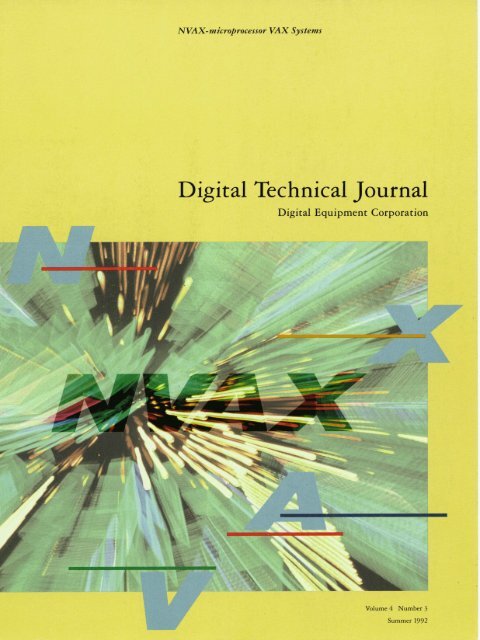
Cover DesignThe WRX microprocessor is Digital's fastest VRX implementationand the common theme ofpapers in this issue. Our cover graphicjoins the WHXproject code name with an image of speed - thechip's most salient characteristic and theperjomzance advantageit brings to a range of new VAxsystm.The cover design is by Deb Anderson of Quantic Communications, Znc.EditorialJane C. Blake, EditorKathleen M. Stetson, Associate EditorHelen L. Patterson, Associate EditorCirculationCatherine M. Phillips, AdministratorSherry L. GonzalezProductionTerri Autieri, Production EditorAnne S. Katzeff, ppographerPeter R. Woodbury, IllustratorAdvisory BoardSamuel H. Fuller, ChairmanRichard W BeaneRichard J. HollingsworthAlan G. NemethVictor A. VyssotskyGayn B. WintersThe Digital TechnicalJournal is published quarterly by DigitalEquipment Corporation, 146 Main Street MLO 1-3/B68, Maynard,Massachusetts 01754-2571. Subscriptions to the Journal are $40.00for four issues and must be prepaid in U.S. funds. University andcollege professors and Ph.D. students in the electrical engineeringand computer science fields receive complimentary subscriptionsupon request. Orders, inquiries, and address changes should besent to the Digital TechnicalJournal at the published-by address.Inquiries can also be sent electronically to DTJ@CRL.DEC.COM.Single copies and back issues are available for $16.00 each fromDigital Press of Digital Equipment Corporation, 1 BurlingtonWoods Drive, Burlington, MA 01830-4597Digital employees may send subscription orders on the ENET toRDVAX::JOURNAL or by interoffice mail to mailstop ML01-3/B68.Orders should include badge number, site location code, andaddress. All employees must advise of changes of address.Comments on the content of any paper are welcomed and maybe sent to the editor at the published-by or network address.Copyright O 1992 Digital Equipment Corporation. Copyingwithout fee is permitted provided that such copies are made foruse in educational institutions by faculty members and are notdistributed for commercial advantage. Abstracting with creditof Digital Equipment Corporation's authorship is permitted.All rights reserved.The information in the Journal is subject to change withoutnotice and should not be construed as a commitment by DigitalEquipment Corporation. Digital Equipment Corporation assumesno responsibility for any errors that may appear in the Journal.ISSN 0898-901XDocumentation Number EY-J884E-DPThe following are tradeinarks of Digital Equipment Corporation:Alpha AXP, DEC, DECchip 21064, DECstation, DECwindows,Digital, the Digital logo, KA50, KA52, KA675, KA680, KA690,MicroV!, MS44, MS670, MS690, Q-bus, Q22-bus, Thinwire,TURBOchannel, lXI'RM, VAX, VAX-11/780, VAX 4000, VAX 6000, VAX7000, VAX <strong>1000</strong>0, VAXcluster, VAX MACRO, VAXstation, VMS, andVXT 2000.MACH is a trademark and PAL is a registered trademark ofAdvanced Micro Devices, Inc.SPEC, SPECfp, SPECint, and SPECmark are registered trademarks ofthe Standard Performance Evaluation Cooperative.SPICE is a trademark of the University of California at Berkeley.TPC Benchmark and tpsA-local are trademarks of the TransactionProcessing Performance Council.Book production was done by Quantic Communications, Inc.
Contents9 ForeiuordRobert id. SupnikNVAX-microprocessor VAX SystemsI IThe NVAX and NVAX+ High-perfomnameVAX MicroprocessorsC;. Michael Uhler, Debra Bernstein, Larry L. Biro,John E Brown 111, Jolui H. Eclrnondson,Jeffrey D. Pickholtz,and Rebecca L. Stamnl24 The NVAX CPU Chip: Design Challenges,Methods, and CAD ToolsDale R. Donchin, Timothy C. Fischer, Thomas E Fox,Victor Peng. Ronald l? Preston, and William R. Wheeler38 Logical Verification of the NVAX CPU Chip DesignWalker Anderson47 The VRX 6000 Model 600 ProcessorLawrence Chisvin, Gregg A. Boucliard, andThomas M. WennersGODesign ofthe VAX 4000 Mode1400,500, and 600 Systm~sJonathan C. Crowell, Kwong-Talc A. Chui, Thomas E. Kopec,Samyojita A. Naclkarni, ancl Dean A. Sovie73 The Design of the VAX 4000 Model 100 andMicroVAX 3100 Model 90 Desktop SystemsJonathan C. Crowell and David W Maruska82 The VAXstation 4000 Model 90Michael A. Callander, SK, Lauren M. Carlson,Anclrew R. Ladd, and Mitchell 0. Norcross92 VAX 6000 Error Handling: A Pragmntic ApproachBri;in I'orter
I Editor's IntroductionJane C. BlakeEditorThe WM microprocessor is a high-performance,single-chip implementation of the VAX architecture.It is today's fastest Vru; microprocessor and the Cl'L1at the hart of the mid-range, low-end, and workstationsystems described in this issue of the DigitalTechnic~zl Journcll.The WtLY chip is not only fast, with cycle times aslow as 11 ns, but also holds a unique position in theDigital family of microprocessors: NVAX is both anupgrade path for existing VAX systems and a migrationpath to Alpha &YP systems. In their paper onthe WAS anel WAX+ chips, Mike Uliler, DebraBernstein, Larry Biro. John Brown, John Edmondson,Jeff Picklioltz, ancl Rebecca Stamm present anoverview of the complex microprocessor tlesignsand relate how RlSC techniques are used in this CIS
Biographies IWalker Anderson Principal engineer Walker Anderson is a member of theModels, Tools, ancl Verification Group in the Semiconductor Engineering Group.Currently a co-leader of the logical verification team for a fim~re chip design, heled the NVAX logical verification effort. Before joining Digital in 1988, Walker wasa diagnostic and testability engineer in a CPU development group at DataGeneral Corporation for eight years. He holds a B.S.E.E. (1980) from CornellUniversity and an M.B.A. (1985) from Boston Universitj!Debra Bernstein Debra Bernstein is a consultant engineer in the SemiconductorEngineering Group. She worked 011 the CI'U design and architect~~refor the NVkY ~nicroprocessor and the VAx 8700/8800 systems and is currentlyco-architecture leader for a future Alpha AXP processor. Deb received a B.S. incomputer science (1982, cum laude) from the University of Massachusetts inhnherst. She holds one patent, has two patent applications pending, and hascoauthored several technical papers.Larry L. Biro Larry Biro joined the Electronic Storage Development (ESD)Group in 1983, after receiving an M.S.E.E. from Rensselaer Polytechnic Institute.While in ESD, he contributed to the advanced development of solid-state diskI products. Larry . ,ioined the Semiconductor Engineering - Grou[> as a custom circuitdesigner on the NVAX E-box. Later, as a member of the NVAX+ chip implementationteam, Larry designed the clock and reset logic, coortlinated back-endverification efforts, and co-led the chip debugging. Currently, he is the project- leader for a future, single-chip ViLv implementation.Gregg A. Bouchard Gregg Bouchard is a senior hardware engineer with theScniiconductor Engineering Group. His current responsibilities include the moduledesign of a DECchip 21064 daughter card that contains a CPIJ-to-bus interface.Previously, Greg worked on chip design of the WAX-to-KVI bus interface for theVAX 6000 Model 600, and field programmable gate array chips for the vmstation4000 Model 90. Gregg joined Digital in 1986 after receiving his B.S.E.E. from theRochester Institute of Technology. He also holds an M.S.E.E. from NortheasternUniversity and has a patent pending related to hardware queue structure.
John F. Brown After receiving an 3.I.S.E.E. from Cor~lell University in 1980,John Brown joined the engineering staff ;it Digital. At present, he is a consultantengineer working on Alph;~ AS]' niicroprocessor advanced development. John'sprevious responsibilities inclutle ni;inaging the tlesign of tlie instruction decotlesection of tlie WAX micropl.ocessoc He ;ilso made technical contributions tothe Viu( 6000 Model 200 ancl 400 chip sets, ;ulcl w:rs Iiardware engineer h)r theextended flo:~ting-point cn1~;incernento the VU-11/780 system. John Iiolcls twopatents antl has seven iipplic;~tions pending.Michael A. Callander, Sr. Michael Callantler is a principal engineer inIligital's Semiconductor Engineering igit:ilincludes tlesign :rncl nrcI1itcctur;rl specification for various CI'U motlules ;mcl systems,incl~iding tlie VfiS 8200 ;ind tlic Vr\S 6000 kloclel 400 and Motlel 500, Mikereceived his B.S.E.E. from the Ilniversity of iMassacbi~setts in 1982 ;incl joinetlDigital upon graduation. He has nuthorecl several technical papers ;incl hiis ;Inumber of patent ;~pplic;ttions pentling.Lauren M. Carlson A senior hnrtlware engineer in tlie Semicontluctor EngineeringGroup, L;~iiren (:;~rlson is cut-rently working on the design of a peripheralchip set for 21 new microprocessor. I'reviously, she tlesigned the Vt\\Sstr~tion4000 Model 90 evelopment Group. She receivetl herB.S.E.E. from Worcester Pol!rtechnic Institute in 1986 and joinetl Digital in 1087Lawrence Chisvin A l>rincip;~l h;~rclw;~re engineer in tlie SemiconcluctorEngineeri~ig Group, L;~rr!,
Jonathan C. Crowell An engineering manager in the Entry Systems BusinessGroup, Jon Crowell was the project leader and system engineer on the VAX 4000Motlels 100,400, 500, and 600 and the MicroVAX 3800, 3900, and 3100 Model 90systems. He is now working on the tlesign of the next generation of ViD( 4000 systems.Previously, Jon worked ill the Systems Integration Group qualiljiing Q-busdevices and DSSI adapters ;~ncl storage devices. He joined Digital in 1986. Jonreceived a B.S.E.E. (1981) and an M.S.E.E. (1986) from Northeastern University. Hehold six patents and is an active member of IEEE.Dale Donchin Dale Donchin manages schematic enti-). ancl layout verificationCAD tool development in the Semiconductor Engineering Group. He facilitatedthe use of CAD tools for NVKX design, primarily for layout and pli)aical chipverification. Dale is presently pcrformlng in a similar capacity for a new microprocessordesign based on the Alpha AXP architecture. He joined Digital in 1978,and was previously a clevelopinent manager in the RSX operating system group.Dale holtls a B.S.E.E. (1976, honors) and an M.S.E.E. (1978) from Rutgers UniversityCollege of Engineering and is a member of IEEE and ACM.John H. Edmondson John Edmondson is a principal engineer in the SemiconductorEngineering Group. At present, he is co-architect of a firture RIS
Thomas E. Kopec Principal engineer Tom Kopec was ;I n1enihe1- of tlie EntrySystems Business Group that designed the \JhS 4000 Nlodels 200 throirgli 600,;lnd the Micro\$= 3500 and 3800 systems. He also led an Alpha ~ ?
Victor Peng Victor Peng is a consultant engineer in the SemiconductorEngineering Group. He received his B.S. in electrical engineering fromRensselaer Polytechnic Institute in 1981, and his M.S. in electrical engineeringfrom Cornell University in 1982. Victor joined Digital in 1982. He was a memberof the design teain for the VAX 8200/8300 memory interface chip and patchablecontrol store chip. He led the implementation of the VAX 6000 Model 400 floating-pointchip and was co-manager of the NV/LY chip design team.Jeffrey D. Pickholtz Jeffrey Pickholtz received an A.S. (1977) in specializedtechnology from Penn Technical Institute and a B.S.E.E.T. (1989) from CentralNew England College. He joined Digital in 1977 as a technician and worked ona variety of midrange computers. More recentl): his responsibilities haveincluded technical contributions to the VAX 6000 Models 400 and 600, and VAX7000 Model 600 chip sets. Currently, Jeff is a senior engineer in theSemiconductor Engineering Group, leading the implementation of a futureCMOS microprocessor chip.Brian Porter As a consulting software engineer in the Systems Group of VMSDevelopment, Brian Porter was responsible for CPU error handling in the VAX6000 family. Prior to this work, he was responsible for support of VAX systemsand was an author and maintainer of the VMS error log utility SYE. Brian is theauthor of the original VMS striping driver, which was later developed by othersinto the VMS striping driver product. He currently works in the Executive Groupof VMS Development and is responsible for symmetric multiprocessing. He hastwo patents pending on memory error handling. Brian joined Digital in 1973.Ronald P. Preston Ronald Preston is a principal engineer in the SemiconductorEngineering Group. Since joining Digital in 1988, he has worked onthe design of several microprocessors. Ron was the circuit design and implementationleader for the E-box on the NVAX microprocessor. He is currentlydesigning the instruction issue logic for a superscalar RlSC microprocessor. Priorto joining Digital, he worked on the design of CMOS microcontrollers forSignetics Corporation. Ron received his B.S.E.E. in 1984 and his M.S.E.E. in 1988from Rensselaer Polytechnic Institute. He is a member of Eta Kappa Nu and IEEE.Dean A. Sovie Design engineer Dean Sovie joined Digital in 1981 and is amember of the Electronic Storage Development Group. He is currently involvedin the battery backup laser memory design. Prior to this work, he contributed tothe design of the high-performance memory module used in the Vhu 4000 Motlel400, 500, and 600 systems. Dean also helped design memories for the VhY 6000,VAX 4000 Model 200, and POP-11 systems. In addition to his present responsibilities,he is pursuing a degree in electrical engineering at Northeastern University.
Rebecca L. Stamm Rebecca Stamm is a principal hardware engineer in theSemiconductor Engineering Group. She led the design of the backup cache, thebus interface, and the pin bus for the NVAX CPU chip. Rebecca then led the chipdebug team from tapeout through final release of the design to manufacturing.Since joining Digital in 1983, Rebecca has been engaged in microprocessor architectureand design. She holds two patents and has seven applications pending.Rebecca received a B.A. in history from Swarthmore College ancl a B.S.E.E. fromthe Massachusetts Institute of Teclinolog)~G. Michael Uhler Michael Ubler is a senior consultant engineer in the SemiconcluctorEngineering Group, where he leads the advanced development effortfor a new high-performance microprocessor. As chief architect for the NVAX andREX520 microprocessors, Mike was responsible for the CPU architecture, performanceevaluation, behavioral modeling, CPU microcode, and CPU and systemdebug. He received a B.S.E.E. (1975) and an M.S.C.S. (1977) from the University ofArizona and joined Digital in 1978. Mike is a member of IEEE, ACM, Tau Beta Pi,and Phi Kappa Phi and holcls eight patents.Thomas M. Wenners Thomas Wenners is a senior hardware engineer in theSerniconductor Engineering Group. He is responsible for the design of a nextgenerationVm workstation CPU moclule and for CPU module designs of DECchip21064 microprocessor-based products. Tom's previous work inclutles the moduledesign of the \ii\X 6000 Model 600, module design and signal integrity supporton ESB products, and analysis and evaluation of advanced chip and modulepackaging. Tom joined Digital in 1985. He received a B.S.E.E. (1985, cum Iaude)and an M.S.E.E. (1990) from Northeastern University.William R. Wheeler A principal engineer in the Semicontluctor EngineeringGroup, Bill Wheeler performed architectural definition work for the NVAXmicroprocessor and was project leader of the NVAX M-box. Prior to this work, hedesigned the I-box unit for the third-generation VLSI VAX implementation. He iscurrently involved in advanced development work for improving custom designtools and methods. Before joining Digital in 1983, Bill received both his B.S.E.E.(198'2) and his M.S.E.E. (1983) from Cornell University. He has coauthorecl threepapers on vLSI designs and holds three patents.
Robert M. SupnikCorporate Consultant,Vice PresidentTechnical Directol;Alpha AXP and VAX SystemsIf, as the popular saying goes, "Once is happenstance,twice is coincidence, three times is concertedaction," then four consecutive instances ofoutstanding engineering achievement must be evenmore significant.Since 1985, Digital has designed, developed, andshipped four generations of leadership VAX microprocessorsand CMOS-based systems:In 1985, the MicroV,%x chip and resulting systems(such as the MicroVAX I1 and tlie Vmstation2000)In 1987, the CVAX chip and resulting systems(such as the MicroVAX 3800, the VAX 6000-200,and the VAXstation 3100)In 1989, the Rigel chip and resulting systems(such as the VAX 4000-300, the VAX 6000-400,and the VAXstation 4000-60)In 1991, the NVkV chip and resulting systems(such as the VhY 4000-500, the VAX 6000-600,ant1 the VkYstation 4000-90)The first three were described in the DigitalTechnical Jozrrnal issues of March 1986, August1988, ancl Spring 1990, respectively; the last is thesubject of this issue.WAX and its systems are the culmination ofeverything Digital and its engineers have learnedabout chip and system design over the last decade.The teams involved drew on many disciplines ofhardware engineering, from microarchitecture towhole-system verification, to produce productsof unparalleled performance and quality. Theresults speak for themselves.From its initial shipment in October 1991through today (a year later), Wh,Y was (and is)tlie fastest shipping CISC microprocessor in theworld, whether measured by clock rate,SPECmarks, or transactions per second.NVAX had fewer bugs after design completion,and went from tape-out to production morequickly than any microprocessor in Digital'shistory.NVAX systems, spanning the range from workstationthrough mainframe, all shipped on orahead of schedule, meeting or exceeding predictedperformance.An outstanding engineering achievement indeecl!The roots of NVAX can be traced back a decade totwo distinct engineering programs: the High-endSystems Group's studies and implementations ofhighly pipelinetl VAX systems; and the SemiconductorOperations Group's projects in processdevelopment and microprocessor tlesign.The High-end Systems Group started work onhighly parallel VAX systems in 1979, designing andbuilding the vAX 8600-the first VAX to includeoverlapped operand tlecotling (see tlie DigitalTechniccil Journal, August 1985) At the same time,a research team tlescribetl HyperVAX, a hypotheticalfully pipelined design Although HyperVU wasnever built, its microarchitecture had a strolig influenceon the design of the VAX 9000, Digital's ECLmainframe (see the Digital Technical Journal, Fall1990). And the microarchitecture of the VAX 9000,in turn, was the basis for WAX.The Semiconductor Operations Group alsostarted work in 1979, formulating a multiyear programfor the development of both semiconductorprocess technology and leading-edge nlicroprocessorsThis program spanned the years 1983 to 1987and encompassed the development of the V-11,MicroVA>( 11, and CVAX microprocessors In 1986,the plan was extended through 1991, encompassingthe development of Rigel, Mariah (a Rigel variant),and a fourth-generation W I V&Y code-named NV..The goals for NVAX were ambitious. First, itstargeted performance was more than 25 timesfaster than the VAX-11/780 (more than 10 timesfaster than the just-introduced CVm chip), requiringsignificant improvements in both microarchitecturalefficiency and in cycle time Seconcl,the chip development scliedule coincided with the
semiconductor process development scheclule,requiring breakthroughs in concurrent developmentof product and process. And tliird, the timeallottccl from chip design conlpletion to systemshipment was tlie shortest in Digital's history,requiring unprecedented accuracy in chip andsystem design and verification.As in past projects, work in various disciplinesseniiconcluctorprocess developnient, chip microarchitectureand circuit design, ~nicroprocessordesign tools, chip anel system verification tools,and system design-cascaded from processthrough systems. First to start was a team fromAdvancecl Semiconcluctor Development (ASD),which designed, simulated, and introduced intomanufacturing CMOS-4, Digital's fourth generationof ClLlOS technology (see the Digit611 R~chnicnlJourfzal, Spring 1992). Builcling on prior technologygenerations,
G. Michael UhlerDebra BemzsteinLarry L BiroJohn E BwnIIIJohn H. EdmorulsonJeffrey D. PickholtzRebecca L StammVAX MicroprocessorsThe IVVM and I\VAX+ CPU chips are higI3-perforinance VM fnzcroprocessors that usetecbnzqzies l~zlditionally nssoci~~ted 2111th RISC nzicroflrotessor designs to dranzaticallylinprove VXXperforrnance. The tu~o cbips)rovide an ztlpgradepath for existingVXX systems and a migration path from VXX systems to the new Alpha A,V systems.The design evolved throzigbout the project as time-to-market, performance, andconzplexity trade-offs were made Special design features address the issues ofdeb~~g, ~nzciintenance, and analysis.The NVAX and WAX+ CPUs are high-performance,single-chip microprocessors that implementDigital's VN( architecture.' The WAY chip providesan upgracle path for existing systems that use theprevious generation of VAX microprocessors. TheWAX+ chip is usecl in new systems that supportDigital's DE
WAX-microprocessor VAX Systenls500, ;uncI 600; :11itl thc V,\S 6000 Moclel 600.".-5')NVV\S supports ;in extern;~l write-l);icl\: ci~chcthat implements ;r clircctory-Ixiscd bro;~tlc:~stcoherence protocol th;it is co11ip;ltible ivitli c;~rlicr\+lS systems Ii'WAS+ is clcsignetl h)r s!rstems t1i;lt use theI>E 21064 nlicroproccssor inll)le~ne~~t;~tjo~iof the i-\I~,li;i hr;i' ;irchitecturc anel is currently useelin tlie \I&i 7000 Moclel 600 ;ind the VAS <strong>1000</strong>0Moclel 600 s!-stems. N\lAS+ supports ;III extern:~lcache ;mcl I)i~s protocol th;it is compatible witli th;~tof the r>Ec:chip 21064 microprocessor. In existingsyste~iis. VAS+ is configi~recl to si~pport ;11i externalwrite-back c;iche tli;~t implements a conelition:ilwritc-update snoopy coherence protocol.11The two
OSCILLATORSERIAL RoM :rlriplThe NVAX and AWAX+ Higb7perfornzul-zc VAX 1Micl-o/~roccs.sor.q1 DCACHE TAGA _*CONTROL*INTERRUPTSSYSTEM CLOCKSDATA RAMSSYSTEMLOGICFigure 2 WAX+ Chip I~zterface Block DiugranzElectrical and Physical DesignProcess technology, clocking scheme, clock frequency,ancl
AROTATORMV$UTCHESFigure -3Block Diagrnnz of tbe NVAx/WAX+ Core
The NVAX and NVAX+ High-performance VAX Microprocessorsqueues, and the branch-related information intothe branch queue.For operand specifiers other than short literal orregister mode, the I-box decode logic invokes thepipelined complex specifier unit (CSU) to computethe effective address and initiate the appropriatememory request to the Mbox. The CSU is similar infunction to the load/store ilnit on many traditionalRlsC machines.The I-box automatically redirects the programcounter (PC) to the target address when it decodesone of the following instruction types: unconditionalbranch, jump, and subroutine call andreturn. The branch-taken penalty is two cycles forany conditional or unconditional branch. To keepthe pipeline full across conditional branches, theI-box includes a 512-bit by 4-bit branch predictionarray. The prediction is entered in the branch queueby the I-box and compared with the actual branchdirection by the E-box. If the I-box predicts incorrectly,the E-box invokes a trap mechanism to drainthe pipeline and restart the I-box at the alternatePC. A branch mispredict incurs a four-cycle penaltyfor a branch that is actually taken and a six-cyclepenalty for a branch that is not taken.The E-boxThe E-box is responsible for the execution of allnon-fJ.oating-point instructions, for interrupt andexception handling, and for various overhead functions.All functions are microcode-controlled, i.e.,driven by a microsequencer with a 1,600-word controlstore and a 20-word patch capability. Since thecontrol store does not limit the cycle time, wechose to implement a single microcode controlscheme, rather than hardwire control for the simpleinstructions and provide microcode control for theremaining instructions.The E-box begins instruction execution basedon information taken from the instruction queue.References to specifier operands and results aremade indirectly through pointers in the source anddestination queues. In this way, most E-box instructionflows do not need to know whether operandsor results are in register, memory, or instructionstream.To improve the performance of certain criticalinstructions, the E-box contains special-purposehardware. A mask processing unit finds the nextbit set in a mask register and is used in the followinginstructions: FFC. FFS, CALLS, CAL1.G. RET, PUSHR,and porn. A population counter provides the numberof bits set in a mask and is used in the CALIS,CALLG, PUSHR, and POPR instructions. In addition,microcode can operate the arithmetic logic unit(ALU) and shifter independently to produce twocomputations per cycle, which can significantlyimprove the parallel operation of the complexinstructions.In addition to riormal instruction processing, theE-box performs all power-up functions and interruptand exception processing, directs operands tothe F-box, ant1 accepts results from the E-box. Toguarantee that instructions complete in instructionstream order, the E-box orchestrates result storesand instruction completion between the E-box andE-box.The F-boxThe F-box performs longword (32-bit) integer multiplyand floating-point instruction execution. TheE-box supplies operands, and the F-box transmitsresults and status back to the E-box.The F-box contains a four-stage, floating-pointand integer-multiply pipeline, and a nonpipelined,floating-point divider. Subject to operandavailability, the F-box can start a single-precision,floating-point operation during every cycle. and adouble-precision, floating-point or integer-multiplyoperation durjng every other cycle.Stage 1 of the pipeline calculates operand exponentdifference, adds the fraction fields, performsrecoding of the multiplier, ant1 computes threetimes the multiplicand. Stage 2 performs alignment,fraction multiplication, and zero and leatlingonedetection of the intermediate results. Stage 3performs normalization, fraction adtlition, ant1 aminiround operation for floating-point add, subtract,and multiply instructions. Stage 4 performsrounding, exception detection, and condition codeevaluation.Stage 3 performs a miniround operation on theresult calculated to that point to determine if a fullroundoperation is recluiretl in Stage 4. 'lb do this, around operation is perfornied on only the loworderthree (for single-precision) or six (for doubleprecision)fraction bits of the result. If no carry-outoccurs for this operation, the remaining fractionbits are not affected and the fill1 stagc 4 round operationis not required. If the full round is notrequired, stage 4 is dynamically bypassed, resultingin an effective three-stage pipeline.Digital Tecbrrical Jottr11a1 Vol. 4 No. Summer 199-3 15
The WAX on61 WAX+ Hi,q/3-l~erfor~nn~zce VAX Micro/~rocessorsimplernentetl by the ~~Cchip 21064 microprocessor.This C-box interface includes the basicinterface control for the external B-cache and forthe memory and 1/0 system. The NVAX+ C-boxreceives read ancl write requests from the M-box.These requests are queued and arbitrated withinthc C-box ant1 result in cache or system accessacross the EI)I\L. The NVAX+ C-box also maintainscache coherency by sencling invalidate requests tothe M-box whcn requested by external logic.The NVLY+ C-box implementation provides manyof the same features and performance enhancementsavailable in the NVAX C-box. Includecl is support forsoftware-programmable B-cache speeds (one-half,one-third, or one-fourth times the CPU frequency)and sizes (128KH to 8MB), write packing, write queuing,and reatl-write reortlering. In addition, theWAX+ C-box supports the newer platforms andincreases the degree to which WAX+ is compatiblewith the IIECchip 21064 microprocessor. NVAX+C-box features include program~nable system clockspeeds, I/O space-mapping, and a direct-mappedoption on the P-cache.A major difference between the WAX and WAX+implementations is in the B-cache coherence protocol.Rather than mandate a fixed B-cache coherenceprotocol, the NVAX+ implementation allowssystems to tailor the protocol to their particularneeds, hW+ cache coherency is implementedjointly by off-chip system support logic and by theCPU chip, with relevant information passedbetween the two over the EDAL bus. To allow cluplicatecache tag stores (if they exist) to be properlyupdated, the NVA)i+ C-box provides information tooff-chip logic, indicating when the internal cachesare updatecl. External logic notifies the NVAX+C-box when an internal cache entry needs to beinvaliclated because of external bus activityExisting systems configure the B-cache to implementa conditional write-update snoopy protocolcarrietl out using shared and written signals on thesystem bus. Writes to sharetl bloclcs are broadcast toother caches for conditional update in thosecaches. A CI'U that receives a write update checksthe NVU+ P-cache to determine if the block is alsopresent in that cache. If the block is present, theB-cache update is accepted and written into theB-cache, ant1 the 1'-cache is invaliclated. If the data isnot present in the P-cache, the B-cache is invaliclatecl.This results in a write-update protocol fordata that was recently referenced by a CPu (andhence is valid in the P-cache) and recluces to awrite-invalidate protocol for data that was notrecently referenced.To accommodate the programmable nature ofboth the system and cache clock frequencies, theNVAX+ C-box supports nine different combinationsof cache and system clock frequencies. This supportallows efficient use of the chip in a wide rangeof different performance class systems.Pipeline Opera tionThe NVAX and WAX+ chips implement a macropipeline.Multiple VAX macroinstructions are processedin parallel by relatively autonomousfunctional units with queued interfaces at criticalboundaries. Each functional unit also has an internalpipeline (micropipeline) to allow a new operationto start at the beginning of every cycle. Thepipeline operation can be logically depicted, asshown in Figure 4.In pipeline segment SO, instruction stream datais read from the VIC. The next VAX instruction componentis parsed, and queue entries are made insegment S1. For short literal and register specifiers,no other processing is required. Requests for furtherprocessing for all other specifiers are queuedto the CSU pipeline, which reads operand baseaddresses in segment S2, calculates an effectiveaddress, and makes any required M-box requestcontained in segment S3. If an M-box request ismade, address translation and P-cache lookupoccur in segments S4 and S5.Instruction execution starts with an E-boxcontrol store lookup in segment S2, followed bya register file read of any required operands insegment S3, an ALU and/or shifter operation in segmentS4, and a potential result store or register filewrite in segment S5. If an M-box request is required,e.g., for a memory store, the request is made in segmentS4; address translation or PA queue accessoccurs in segment S5; and a P-cache access occursin segment S6.Floating-point and integer-multiply instructionexecution starts in the E-box, which transfers operandsto the F-box. The four-stage F-box pipeline isskewed by half a cycle with respect to the E-boxpipeline, beginning halfway through segment S4.The fourth segment of the F-box pipeline is conditionallybypassed if a full-round operation isnot required. The result is transmitted back to theE-box, logically in segment S5 of the pipeline.Pipeline bypasses exist for all important casesin the I-box and E-box pipelines, so that there areDigital Technical Jorrrrral Vo1. 4 No. .j! Sttrn~ner I992 17
NVAX-microprocessor VAX SystemsINSTRUCTION FETCH,DECODE, SPECIFIER €VAL,MEMORY REQUESTSO S1 52 S3 54 S5 S6VICREADINSTNPARSEOPERNDREADADDMEMREQTBP-CACHEINTEGER, LOGICALINSTRUCTION EXECUTIONFLOATING-POINTINSTRUCTION EXECUTIONKEY:SSPECIFIER EVALINSTNOPERNDMEMREQTBSEGMENTSPECIFIER EVALUATIONINSTRUCTIONOPERANDMEMORY REQUESTTRANSLATION BUFFERALUCSEXPON DlFFALIGN, FRMULTNORM, FRADDBYPASS ROUNDARITHMETIC LOGIC UNITCONTROL STOREEXPONENT DIFFERENCEALIGNMENT AND FRACTION MULTIPLYNORMALIZATION AND FRACTION ADDITIONRESULT ROUNDING AND BYPASSno stalls for results feecling directly into subsequentoperands. The M-box processing of memoryreferences initiated as a result of operand specifierprocessing by the I-bos is usually overlappetlwith tlie execut~on of the previous instruction inthe E-box, witli few or no stalls occurring onP-cache hit.Design Evolution and Trade-08sThe N\Wi and W !+ chips are tlie latest in a line ofCMOS VM microprocessors designed by Digital'sengineers and represent a continuing evolution ofarchitectural concepts from one irnp1ernent;ltionto the next. The preceding chip clesign was theCPrJ for the VAX 6000 Model 400 system.I2 To meettlie time-to-market ancl performance goals, wehad to modify the NV~U/NVAX+ design throughouttlie project.One of the early vehicles for making tlesigntrade-offs was the WAX performance model,which predicts CPIJ and system performanceand aids in quantifying the performance impactof various tlesign options. The performancemode.1 is a detailed, trace-clriven motlel which canbe easily configuretl by changing any of ;I varietyof input parameters. The modcl stimuli usedwere 15 generic timesharing ancl 22 benchmarkinstruction trace files that were captilredby running actual programs on existing VAXsystems.The followi~ig sections describe tlie evolutionof the chip design, including the number of chips,the pipelining technique used, and various cacheissues.N~~rnDer of CPU ChipsThe VLY 6000 Model 400 core CPIl in~l>lemenrationis a three-chip design: a processor chip, with asm;~ll on-chip primary cache; a floating-point chip;and a secondary cache controllel; with internalcache tags. The initial attempt at NVLY CPIJ definitionwas a two-chip design. One chip containedthe I-box (with a 410 VIC), the E-box. the F-box, andthe Mbos (witli a ~GKB, direct-mapped P-cache).The second chip held the C-box ant1 the B-cache tagarray. The project design goals, especially time-tomarket,let1 to a single-chip solution. rather thana two-chip design.To condense the design from two chips to one,we halved the sizes of the Wc; ant1 the P-cache andrnovecl the R-cache tags to external static UMs,leaving the B-cache controller on-chip. Later, wewere able to reduce the penalty of halving the sizeof the I-'-cache by making it two-way set associativerather than direct mapped. With these changes, theperformance moclel showed a performance loss ofless t11;1n 1.4 percent across all the traces, relativeto the two-chip design, with a worst-case pen~ltyof 3.9 percent.There ;Ire strong z~dvantages to the single-chipsolution.Designing a single chip takes less time.This design requires the production ancl maintenanceof only one design database and onemask set.Latency to the B-cache is shorter.An off-chip tag store provides more flexibility inH-cache configurations.
The WAX' and /WAX+ High-performance VAX 1~4icro,!1rocessorsMacropipeliningRun-time perfortnance is the product of the cycletime, the average time to execute an instruction(cycles per instruction [CHI) ant1 the number ofinstructions executed. CMOS process improvementsmade it possible to decrease the hViu;/N\iiU(+ cycle time with respect to the previous generationof ~a microprocessors, thus improving thefirst factor in run-time performance.The VM 6000 Model 400 CPU design uses traditionalmicroinstruction pipelining, i.e., micropipelining,to achieve some amount of overlap andto decrease the CPI. However, using micropipeliningtechniques would not reduce the WAX/N\IN(+
WAX-microprocessor VAX Systemsit ;I subset of the extrrn;rl cache. Exter~lall!~ origin:itetlinv;~litl;~te requests are forwartletl to the1'-c;rche only when the block is it1 the extern;ilc;icIie. Tliis mininiizcs the number of 1'-cache cyclesspent processing invalidate requests. The two-wa!-set-;~ssoci;~tive P-c:~clie might have been slightl!,more effective if it were not a subset of the 1;irgerdirect-nlapped extcrn;il cache. However, this effectis far less significi~nthan tlie effect of expencling ;I1'-c;~clie cycle for every external invalidate event.Virtu;~l c;iches :itmost always have lower l;~tencytlxrn pliysic;~l c;~ches ant1 usually do not require ;ttledicatetl translation buffer. The VrU( architecturesupports the use of ;I VItl:lted with recent writes by tlie (:H: contiiiningthe Vlc:, or 1)). ;in! other (;l-'U. However, solilemec1i;unism must be clefined to make the \'I(; coherentwith the d;it;~ sLrc;tni. In the \Iu architecture.the execution of thc \:tY return from interrupt orexception (1ll:l) instri~ction performs this function.We chose to perfi)rm a complete flush of the \'I(;as p;irt 01' the execution of every RE1 instruction.Rec:~use an IlEI a11v;iys follows a process contextswitch, ;I Flush tluring ;ln llEI removes the processspecifjcvirtu;il ;itltlrcsses of the previous process ;~ntlprevents conflict with (potentially identical) virtu:~l;~tltlresscs for the new process. We coultl have alsochosen to keep tlic \/I(: coherent with the data stre;lnl;~ncl implement per-process qualifiers th;it woulclhave matle per-process virtu;ll atldresses unique.Howevrl; coherence would have requiretl both. :ininv;~liclate aclclrcss ;~ncl :I control path to the VIC. : I I ~some h)rm of backm;~p to resolve \,irtii;rl ;~dtlress;II i;~ses. I'cI--process qi~:~l ifiers would h;ir.e requiretla vr\X ;~rchitecture ch;inge ant1 significant operi~tings!.stenl software ch;~nges. To reduce project risk,we chose to flush the VIcnchm;~rks, fit entirely in a c;lcIie \vhose size js512Kll or less, resulting in slightly better 1,erh)rm;ince.However, many common app1ic;ttionsutilize more memory than will fit in such c;~ches;incl benel'it more from an external cache whosesize is IMI) to 4hI13, elm with the atldition;il I;~tencyinvolvctl. As ;I result. OLI~system designs use 1;lrgerbut slightly slower external cache configu~~tions.Block Size1)uring tlie analybis of the previous generationof \twvicles ;I goocl Ixilance between fill size ;ind theni~mber of cycles I-equired to tlo tlie fill, give118-I)ytc fill tI;it;i 1~1tl~::.I'or comp~tibilit)- with installed s)lstetiis, the sizeof the N\hX external cache block ancl the c:ichefill size is 32 Rytes. On NVILY+. the extern:~l c;icheI>loch: size rn;ilr be 1;lrgt.r and js (74 bytcs j ~ the i V,\X7000 Wlotlel 60(.) :~ncl\:\S <strong>1000</strong>0 hlotlel 600 s).stcms.Ilcc:~usc both s!-stems irnpiement low-latencyrne1lior\. ;ind high-b:tritlnridtll buses, the incre:lse inextcrn;ll c;lclie block size results in betterpcrform:ince.l ill. -1 .GI..i SII~IIIIIL,I. 133.2 Digital Tec6rricnl Jorrrrrnl
X riizd NVAX+ ~ //R~-/I~~O~'II?L~IZCC VAX iWicro/)l-occssorsSpecial Feal-uresThe NV~IX'/NV~\\S+ design inclutles several fe:tturesthat supplement core chip fi~nctions by providingacldetl value in areas of debug, syste~n ~naintenance.and syste~ns ;III;I~J'S~S. Among the features are tliepatchable control store (P(:S) and the perforniancemonitoring hardware.Pntcli~nbLe Control StoreTlie 1x1s~ m;~cliine micrococle is stored in a ROklcontrol store in the E-box. Tlie 1,600-micro.rvortlc;cp;ccity of the E-box controls niacroinstructionexecution and exception hitnclling. 'The l'
NVAX-microprocessor VAX Systemsan ititerrupt. Tlie interrupt is serviced in ;I ~iorm;~lway, i.e., between instructions (or in tlie rnitltlle ofinterruptible instructions) and at an architecturallyspecifietl interrupt priority level. Unlike other interrupts,the performance monitor logic interrupt isserviced entirely in microcode ;~ntl then dismissed;no software interrupt handler is required.The microcode component updates the countersin memory when it services tlie performance monitorinterrupt. During a counter upd;~tc, the ~ilicrocodetemporarily disables the cou~iters, reads ;lndcle;~t-a tlie li;~rclware counters, ~~pdates the countersin ~iie~iior): enables the counters, ;ind rcsumesinstructio~i execution. The b;lse ;itldress of tliecounters in memory is taken from ;I system vectort;tble ;~nd offset by the specific
A. Dipace, C. Dobriansky, D. Donchin, R. Dutta,1). DuXlrne): J. J. Ellis, J. l? Ellis, H. Fair, H. Feaster,T: Fisclie~; T. Fox, G. Franceschi, N. Geagan, S. Goel,M. (;ow;ln, J. Grodstein, I! Gronowski, W Grundmann,H. Harkness, W Herrick, R. Hicks, C. Holub,J. Muhcr, 11. Jain, K. Jennison, J. Jensen, M. Kantrowitz,R. Kh;lnna, R. Kiser, D. Koslow, D. Kravitz,K. Ladd, S. Levitin, J. Licklider, J. Lunclberg,R. Marcello, S. Martin, T. McDerniott, K. McFadden,B. McGee. J. illeyer, M. Minardi, D. Miner, E. Nangi;~,L. No;~ck, T. O'Brien, J. Pan, H. P;lrtovi, N. 1';1tw;1,V: I'eng, N. Phillips. R. Preston, R. Razdan, J. St.Li~urent, S. S;~mudrala, B. Shah, S. Sherman, W Sherwootl,J. Siegel, K. Siegel. C. Somanathan, C. Stolicny,P Stroppaso, R. Supnik, M. Tareila, S. Thierauf. N.W~cle, S. W~tkins, Wl Wheelel; G. LVolrich, and Y. Yen.References1. R. Hrunnel; ed., ViM' Architecture Referenceit.lcirz~~al, Second Edition, (Betlfortl, NLA: DigitalPress, 1991).2. D. Dobberpuhl et al., "A 200MHz 64bDual-Issue CMOS Microprocessor," IEEE Inter-~zaliorzal Solid-State Circziits Co~zference,Digest of Technical Paj~ers, vol. 35 (1992):106- 1023. R. Sites, ecl., Alpha Architecture ReferenceMlnn~lal, (Burlington, MA: Digital Press, 1992).9. L. Chisvin, G. Bouchard, and T. Wenners, "TheViUC 6000 Moclel 600 Processor," DigitalTechnicc~l Jounzcll, vol. 4, no. 3 (Summer1992, this issue): 47-59.10. A. Agarwal et ill., "An Ev;~luation of DirectorySchemes for Cache Coherence," Proceedingsof the 15th An~zclal International Sjjmnposiurnon Cot7zputer Architect~we (May 1988):280-289.11. I? Stenstrom, "A Survey of Cache CoherenceSchemes for illultiprocessors." Collzputer(June 1990): 12-24.12. H. Durtlan et al., "An Overview of the ViU(6000 Model 400 Chip Set," Digital TechnicalJournal, vol. 2, no. 2 (Spring 1990): 36-51.13. VAX 6000 Datcicelzter Systenzs PerJor~nanceReport (Maynard, Mi\ Digital EquipmentCorporation, 1991)4. 0. Fite, Jr. et al., "Design Strategy for the Vfi9000 System," Digital Technical Jo~lrncll,vol. 2, no. 4 (Fall 1990): 13-24.5. W Antlerson, "Logical Verification of theWitY CPU Chip Design," Digital TechnicalJournal, vol. 4, no. 3 (Summer 1992, thisissue): 38-46.6 M. Callantler et al., "The Vhystation 4000Motlel 90," Digital Technical Journal, vol. 4,no. 3 (Summer 1992, this issue): 82-91.7 J. Crowell and D. Maruska, "The Design of theVAX 4000 Nlodel 100 ant1 MicroVAX 3100 Model90 Desktop Systems," Digit611 TechnicalJo~frnal, vol. 4, no. 3 (Summer 1992, thisissue): 73-81.8. J. Crowell et al., "Design of the VIIX 4000Model 400, 500, and 600 Systems," DigitalTechniccll Journal, vol. 4, no. 3 (Summer1992, this issue): 60-72.Digilrrl Zechrricrrl Jour~znl Vol Q iVo 3 \rrtttttter IYW 23
Dale R. DonchinTimothy C. FischerThomas E FoxVictor PengRonald E! PrestonWilliam R Wheelerme NVAX CPU Chip:Design Challenges,Methods, and CAD ToolsThe ArVAX (PL1 chip is 0 1.3 117rlllol1 trc~~zsisto~ 12S I?IICI'O/II'OC~SSOI. desrgizedill Digital's 0 75-11zio.orrzeter 6110.Y-4 tecl~rzologj! It has a tjpic~11 cjlcle ti112e oj'12 ns u~zde~. worst-case operating conditio~zs. The goal of the cl~ip design teallzwas to design a high-pe~$)rrrzmzce, robust, n12d reliable chip, z~itl7irz the constmirftsof n short scl?ecl~~le Design strategies zilere clez~eloped to uchielle this goal,inclz~ding ouga/zizalion of a ~hly desig~zJloiu n~zd 11ez11 il~~l~kl?rozt~~tro~i and ilerlficationneth hods 1Veio pr*ol)rletllry CAD tools also plqyed i/rzlIot~t~llnt roles in thech@ deieoelopr~zent.The N\RX CPU chip is a 1.3 million transistor, \lkYmicroprocessor clesignecl in 1)igital's 0.75-micrometerhmrtli-generation coniplen~ent;lr)~ metaloxitlesemiconductor (
The NVAX CPU Chip: Ilesig~z Cl.alle?zges, ~l~etl~ods, and CAI1 7holsF-BOXL+E-BOXDesign Goals and ConstraintsOur design goal was to develop a high-perform:~ncechip that is electrically robust ;rnd reliable. We hadto accomplish this within the 10S-4 processconstr;~ints ;~ntl the design time :illottecl by thedevelopment schedule. 011s initial implenientntionscheclirle was based on schetluling metrics fromprevious designs. Due to competitive marketingpressures, this schedule was substantially reduced,making it significantly more aggressive than for previousclesigns. Our cycle time was constr;iinecl toa maximum of 14 ns untler worst-case conclitions.Electric;il reliability h;icl to be guaranteed for cycletimes clown to 10 ns ~incler worst-case conditions.
NVm-microprocessor VAX systemsTable 1 Summary of Chip FeaturesTransistors1.3 millionDie size16.2 mm by 14.6 mmCycle time12 ns (typical)Signal pads 261Supply pads 121Package339 pin THPGA*Power dissipationat 12 ns14 W (average)Note: "Through-hole pin grid arrayLlnsed on
The NVA X CPCI Chip: Design ChallenLqes, &lc.tl~ocls, and CAD ToolsIAND MICROARCHITECTURALRTL MODEL ANDCHIP FLOOR PLANIdetailed box-level floor pl;lns. All floor plans wereentered directly into the layout tlat;lb;lse and maintai~ietlthroughout the project. Trdcking the floorplan ;~t severr~levels eased the tlifficulty of integratingthe box l;lyouts to form tlie full-chip compositelate in the project. More details on floor plans ilntlthe use of
WAX-microprocessor VAX systemsCYCLE TME (RELATIVE TO DESIGN TARGET)Note: Oala is normalized based on 14-ns design larget.The cycle tlme of 1.0 equals 74 ns1 I . I 1 1 - i NTV flistog1~111zSI'I(:E, all c1uestion;tble p;tths fl;~ggetl b!~ N'1.v \\/eresimulatecl ubing SL'ICE. Those that were foi~ncl to hcslonl were retlesipnecl to meet the target c!.cle time.Logic ;inel circuit chatiges resulting from tliescan;llyscs ;tntl the in~j>;~ct of these changes on otherdesign represent;ttions ;~ntl verific;ltion tests weretr;~clictl on the electronic b~rllctin bo:~rcl. Since m;cnypeople were worliing 011 tlie clesign sin~ult;meousl):tlet;tiled trxking of changes ;inel oj>en issues pr~\~cdcruci;tl to meeting oirr scl~vtlule. A single ch;~r~gcof cu recli~irrcl 1i1odific;ttion ;~ntl rcverific;ttion ofthe IU'I. moclcl. scliem;itics, I;~)~out, verification tests,anel in some cases tlie chil-, testu;~l specification.Ltyout design proceetletl on :I subbox, or section,b;tsis. A t!.l,ical sectiori consistctl of ;~pprosim;~tclyren rel;ttctl sc1iem;ttics. hch scction was clieckctlfor con~iccti\;it!~ itntl correctness ;lfter its layout \v;~scoml,leted. Sections within ;I box were then integrated:~nd vcrifietl (boxes cont:~jned from 5 to I5sections) hcfor-e the complete chip composite w:ts;~sse~nl,lctl.Scl1enl:ctic i'crification :~ncl I;t).out design wcrcperfornlecl concurrently tluring much of the pnjject.Although this overlap lctl to desig11 c11;111gest11;lt incre;lsccl the amount of I;~yout rework, thechi17 tlevelol,ment schetlule \voultl have been significantly(ongcr if schem;ttic verific;ltion and I;~yo~ttelesig11 h;icl been done seri;~lly. L;i!-o~tt design tool; tlic, precise monitoring of the floor plan wascritic;~l. From the earliest :II-e:~ estimates, it \+/;ISclear th;~tlie chip size was close to the m;~sim~rmth;ic the (:h[0~-4 technology coultl support. We h;~dto ensure that tlie die clitl not cxceed the technologylimit.Prelimin;rry estimites of the tiit. ;trea were m;~cle byextrapo1;ltions from previous
areas were in tlesign. Since layout clid not existfor tlie control blocks.
\ ILOWER PAD CLOCKS (MJ)NVAX-microprocessor VAX systemslines, each 17 ~iiicrometers wide. Vertical met;~ltwo (M2) .lines are usecl to strap the power lines;lntl form a t;, grid and a y., grid. The ant1 1;distribution of the left-li;i~id side of the chip w;isdifferent from that on tlie riglit bec;iiise of the speciallayout requirements of the cache ;crr;lys ant1 theF-box.Indivitlual cell layout tlitl not cont;~in MS. Thepowel-, groirncl, and clock connections for a cellwere routed by short vertical 1M2 lines inside eachcell. These iM2 lines were connected to the Mjgrids automatically by a CAI> tool.On-chip Clock Distributio~zIn ortlcr for 11s to meet the perform;itlce go;~ls, itwas critic;~l to keep clock skews small ant1 edgerates sh:irp across the chip. As shown in Figure 5,special attention w;is given to the clock distributionscheme. Differential outputs 1-'rom ;ui off-chiposcillator were sul~plied to a receiver locatecl at thetop of the chip. The output of the receiver wasroutecl to the global clock generator (
The NVAX CPU Chip: Design CL7allenges, ~llethods, and CAD Toolsincrease their driving capability. The clocks werethen distributed, using the low-resistance thirdmetal layer (17 milliohms per square), from the topto the bottom of the central clock routing channelthat spans the chip.Clocks were supplied to the different functionalboxes by locally tapping off the central clock routingand buffering each signal with four inverters tofurther increase the signal's driving capability. Thisbuffering helps to minimize the capacitive loadsseen by the clock phases in the central routingchannel in which the RC delays are held to 30 picoseconds(ps). To reduce distribution skew betweenthe global clock lines, loading on each global linewas balanced by adding dummy loads to the morelightly loaclecl lines. The buffered clock phaseswere distributetl to the east and west of the centralclock routing channel, again using M3 to reduce RCdelay. The east-west clock routing was strappedwith M2 as shown in Figure 5. These straps werenot allowed to cross box boundaries. Box-levelclock skew was reduced by using a commonsection buffer design ancl layout, ancl by carefilllytuning the buffer drive capability to the clock Loadin each section.Finally, before the clocks were usecl by the logic,the clock signals were locally buffered. These finalstages of local buffering served two purposes: theyrecluced the gate loading on the east-west clockrouting, and they helped to sharpen the clock edgesseen by the logic.The global clock routing network was spaced sothat the RC delays of local clock branches woulclnever exceed a negligible 125 ps. \Ye calculated theRC delays of local clock branches using the W~WoTHlayout interconnect analyzer (described in thesection New I'roprietary CAD Tools) and, wherenecessary, rerouted branches to meet the 125-psdesign goal. A sample RC plot, generated byWAWOTII. for a section of local clock routing, isgiven in Figure 6. The clock skews and edge ratesacross this 1.62-centimeter chip are less than 0.5 nsand 0.65 ns, respectively.Microcode Control StoreThe design of the 12KB RO&l control store was simplifieclby dividing it into four subarrays. Each subarrayhas its own M1 bit lines. The M1 bit lines fromthe subarrays are cascacled onto low-capacitanceM3 super bit lines that extend over all four subarrays.Since the capacitance of the 1M3 super bit linesis low, the access time is very fast, obviating theneed for sense amplifiers and voltage reference generators.This substantially recluced the timerequired to clesign and verify the control store 1m)hl.Primary CacheA similar technique was used in the 8KB P-cache toease the timing requirements. The three high-orclerP-cache address bits must be translated and consequentlybecome valid later than the untranslatetllower-orcler bits. By dividing the P-cache into eightsubarrays, each with its own sense amplifiers, thecache subarray access can be started before thethree translated address bits are valid. When thelast three address bits become valid, the outputs ofthe subarrays are multiplexed onto the M3 super bitlines, resulting in a faster cache access time.Layout Vmification ToolsVerifying the WAX chip layout presented severalCAD software challenges. Prior to the NVhs design.the existing layout verification tools were able toextract full-chip netlists from layout for all largedesigns in a single batch process. However, theexisting layout netlist extractor could not hanclledesigns such as NVhK with over one nlillion transistors.Also, a more accurate capacitance extractionalgorithm was required to calculate side-to-side ant1fringing capacitance, which came to show significanteffects in the small physical dimensions inC&IOS-4. Furthermore, accurate interconnect resistanceextraction was needed for NVAX. A combiniltionof new CAD tools (see Figure 7) and designmethods was employed to meet the WAX layoutverification requirements.Partitioning Using "Clean Belts"To address the problem of extracting parasiticcapacitance data from such a large design, the WAYchip layout was constructecl so that each chip partitioncould be indepenclently extracted withoutintroducing inaccuracies in the results. The chipwas partitioned into nonoverlapping regions, eachof which had a rectilinear annulits or "clean belt"around its periphery. A clean belt is a rectangularregion that contains only metal lines and satisfies ;Inumber of layout design rules beyond those set bythe technology. The clean belt layout rules preventeddesign rule violations within the clean beltand between adjacent clean belts. The rules alsoensured that extracting parasitic capacitance froma region enclosecl by a clean belt could be doneDigital Techiticril JourrcrrlVol 4 No .; J~r~unrer 1992 3 1
WAX-microprocessor VAX systemsNole: Times are given in picoseconds;~ccur;~tely reg:irclless of the m:~trrials that borderthc region. Partitioning the chip in this mannernlatle it easier to locate glob;~l wiring errors.Hic.t"n~-cl?icc/l Netlist Extr~~ctiol?f\ new netlist estractor, HILES, \\i:~~ LISCCI to meet thehigh d:it;i capacity requirements of the NVAX niicro-~rocessor. H1I.M is more efficient th;m the previousin-house netlist extractor bec;l~lsr it recognizes 1:iyout cell inst;i~~ces :11ic1 in many cases needs toextract cell-orily tlcl'initions. 111 contrast, the previousrietlist extractor "fl;ittetletl" the layout data intoone tio111iierarchic:rl cell and, therefore. extr;~cteclall data witlio~~t re~rsi~ig previoi~sly extractetl cclldefinitions. The :ict~r;il ~,erh)rmance inipro\lementrealized by H1I.I.S tlepe~ltls on the hierarchy of thecllip layoi~t clcsign. If very I'ew cells are replic;~tetl.or cells ;ire rcplic:~tetl in ;I way that recllrires the
The W AX CPU Chip: Design Challenges, Methods, and CAD ToolsI LAYOUT ICUPF -ItHlLEXJttRESISTANCE*WAWOTH1 1Figure 7 Simplified Layout Verification Tool Flowextractor to explode the cells (i.e., create more flatdata) to extract them properly, then minimal performanceimprovements are seen. An example ofthe latter situation is an array of a repeated pair ofoverlapping cells that forms one or more transistorsdue to the overlap (one cell contains diffusionareas that become source and drain regions whenoverlapped with the other cell, which containspolysilicon lines that become transistor gates).Several layout design guidelines were defined toensure that performance improvements from usingHlLM would be realized. Adherence to the guidelinesminimized situations that require HILEX toexplode cells and encouraged the use of hierarchyin the layout. However, since it was not always possibleto adhere to these design recommendations,HlLEX was designed to handle large amounts of flatdata.The chip netlist was extracted from the completechip layout prior to tape out. This presented quite achallenge since even with the use of HILEX, extractingthe chip netlist from the 225MB chip layout filein one pass required more than the maximum oftwo million virtual pages of memory allowed by theVMS operating system architecture. To go beyondthe VMS virtual memory limit, the internal memorymanagement routines within HILEX were modifiedto allocate additional heap from the process stack(in P1 space) when the VMS memory allocationroutines indicated that PO memory space wasexhausted. This technique was used to allocate the2.5 million virtual pages required for fuI I-chip connectivityextraction.Netlist Co~nparisonA utility called WLC was used to verify that netlistsextracted from layout by HILEX matched netlistsgenerated from the chip schematics. Since theNVAX schematic hierarchy rigorously matched thelayout hierarchy only at certain levels, the connectivitycomparison was performed flat, wLCemployed a graph-building and graph-traversingalgorithm that worked well for comparing less than500,000 device connections. However, substantialpaging occurred when comparing larger netlists.Since the NVXX chip contained 1.3 million devices,the performance of K C was inadeqtiate for fullchipnetlist verification.Digital Tecbnical Journal Vo1. 4 No. 3 Summer 1992 33
NVAX-microprocessor VAX systemsTo improve the elapsed time of netlist co~np;~risonb;ltch jobs, ~liultiprocessing was employed.HILEX was moclified to write the extracted netlist ofthe clean belt partitions. Each partition was thencompared by WLC, in parallel on multiple CPlls, toits ec1uiv;llent schematic-generated netlist. Thisappro;lch reduced the total elapsed time for theI\IVrU( chip netlist comparison from more than threedays to seven I-lours. Cross-reference files output byW1.C: ;tncl the schematic netJists were processecl by ;Iseparate program, MATCH-CHECKER, to verify theconnectivity of nodes that crossed partition boundaries.This ;rdditional step added only eight minutesto the total elapsed time for comparing chipnetlists.Capacitance ExtractionThe small spacing dimensions of the submicro~l
The WXX CPU Chip: Design Challenges, Methods, and CAD ToolsTable 3 REX Extracted Parasitic ResistanceData and Batch Run-time Data forNVAX BoxesExtraction TimeBox Resistor Count (Hours)New Proprietary CAD ToolsSeveral other novel CAD tools were specificallydesigned for the NVAX chip. These tools providedpractical solutions to verification and analysis problemsthat were previously unmanageable orintractable.CWGO Logic SimulatorCHANGO was an important development for NVAXfunctional verification because it allowed significantlymore simulation cycles and functionalverification tests to be performed from the WAXtransistor-level clescriptio~l than was previouslypossible. CHANGO is a two-state gate-level logicsimulator designed to maximize performancethrough compiled, straight-line simulation. Electricalissues such as gate delay and charge sharingwere not modeled since CIWGO was usedfor functional, not timing, verification. CHANGO'sparallel simulation capability allowed the sirnultaneousexecution of 13 different NVAX moclelsimulations on one CPU, which resultecl in an eightfoldincrease in simulation performance. Overall,CHANGO has been shown to accelerate simulationone to two orders of magnitucle over traditionalevent-driven gate-level simulators. Its high throughputenabled us to boot the vMS operating systemtwice (75 million cycles) prior to tape out.To create a CHANGO moclel, a transistor-levelnetlist description of the design was input to a preprocessorcalled
WAX-microprocessor VAX systemsmodel was i~setl for other structures." NTV flr~ggedcircuits that hiletl to meet tlie itlentifiecl timingco11str:lints within ri user-specified time toler;lnce.Like other static tinling verifiers, sonie paths identifiedby N n were "don't cares" or were logicallyimpossible. The user eliminated these false patlisby tleleting timing constraint checks or by specifj.-ing niutu:ll exclusivity between specifietl groups ofnodes.WA WOTH Interconnect A nnlyzer'Fradition:~I ni;unu;ll techniques for checking R tools211 lowed LIS to complete tlie NVLY CP'LJ chip tlesign in30 percent less time than our initial schedule hat1required. Typical parts operate at 8.3.3 MHz (a 12-11scycle time) under worst-case conditions for temper;lturc;lnd power supply This is 2 ns better tli;~tio ~ nl;~xi~ni~ni~ r cycle time design constraint. Thechip bootetl the VMS operating system ten claysafter the first prototype wafers were available, :mdbooted the IILTRIX system a few days I;tter. Multiprocessingwas ri~nuing within weeks. Fifteenobscure logic bugs were found in the first-p;~sschips. but none of them impeded system debug orprototype development. No circuit design bugswere founcl. Only one design revision was neetledprior to \~olunie chip ~il;u~iufact~~ring.
The NVAX CI'U Chq~: Design Challenges, ~MElhods, aizd CAD Tools2. B. ZetterJuncl,J. Farrell, and T. Fox, ra micro processorPerformance and Process Complexityin CMOS Technologies," Digit~il TechnicalJourizal, vol. 4, no. 2 (Spring 1992): 12-24.3. J. Crowell, K. Chui, T. Kopec, S. Nadkarni, andD. Sovie, "Design of the \rN( 4000 Model 400,500, and 600 Systems," Digital TechnicalJounzal, vol. 4, 110. 3 (Summer 1992, thisissue): 60-72.4. L. Chisvin, G. Bouchartl, ancl T. Wenners, "TheVAS 6000 Model 600 Processor," LligitalTkclnizical Jo~lrizal, vol. 4, no. 3 (Summer1992, this issue): 47-59.5. R. Batleau et al., "A 100 MHz MacropipelineelVtOC CMOS Microprocessor," Accepted forpublication in IEEE .loul-izal of Solid StateCirc~lits, vol. 27,110. 11 (November 1992).6. SPICE is a general-purpose circuit simulatorprogram developed by Lawrence Nagel antlEllis Cohen of the Department of ElectricalEngineering and Computer Sciences, Universityof California, Rerkeley.7 T. Fox, I? Grononrski, A. Jain, B. Leary, andD. Miner, "The CVAx: 78034 Chip, a 32-bit Seconcl-generationVN( Microprocessor," DigitcilTechniccll Jo~lrizal, vol. 1, no. 7 (August 1988):95- 108.8. W Durdan, W. Bowhill, J. Brown, W! Herrick,R. Marcello, S. Samudrala, G. tlhler, andN. Wade, "An Overview of the \IILY 6000Moclel 400 Chip Set," Digital TechnicalJounzal, vol 2, no. 2 (Spring 1990): 36-51.9. J. Hwang, "REX-A VLSl Parasitic ExtractionTool for ElectronligEdtion and Signal Analysis,"28th Design A LI torncf tioiz Conference (1991):717-722.10. J. Pan, L. Biro, J. Grodstein, B. Gruntlmann,antl Y. Yen, "Timing Verification on a 1.2M-Device Fu l I-Custonl
Walker Anderson ILogical Vmication of theWAX CPU Chip DesignDigitalS AVRX high-perfonnance inicl-oprocessor has ct co?~zple.x logical design.A rigorous simulation-based uerific~ition effort was ~~rzdertakeiz to ensure th~ltthere zilere no logical errors. At the core of the effort were inz~llelnent6~tiolz-orie1zted,directed, pseudorandom exercisers. Tl~esexercisers were supplemented with inzplementation-specificfocused tests and e-ristirzg VRX architectural tests. Only 15 logicalbugs, all unobtrusive, were detected in the first-pass design, and the operatingsystellz booted with first-pass chips in a prototype system.The WAX CPU chip is a highly complex VAX microprocessorwhose design recluiretl a rigorous verificationeffort to ensure that there were no logicalerrors. The complexity of the design is a result ofthe advanced microarchitectural features that makeup the NVkV architecture, such as branch prediction,micropipelining and macropipelining techniques,a three-level hierarchy of instructioncaching, and a two-level hierarchy of write-throughand write-back tlata caching.' Also, the chip was initiallyintended for two different target system configurationsand had to be verifiecl for operation inboth. Product time-to-market goals mandated ashort development schedule relative to previousprojects, and there was a limited number of verificationengineers available to perform the tasks.The verification team set two key goals. The firstwas to have no "show stopper" logical bugs in thefirst-pass chips antl, consequently, to be able toboot the operating system on prototype systems.Meeting this goal would enable the prototypesystem hardware ancl software developn~enteamsto meet their schedules and \voultl allow moreintensive logical verification of the chip design tocontinue in prototype systems. The second keyteam goal was to design second-pass chips with nological bugs, so that these chips could then beshipped to customers in revenue-producing systems,meeting this goal was critical to achieving thetime-to-market goals for the two planned NVAXbaseclsystems.Team Organization and ApproachLogical verification was performed hy a team of engineersfrom Digital's Sen~iconductor EngineeringGroup (SEC) whose primary responsibility was todetect ancl eliminate the logical errors in the NViOLdesign. The detection and elimination of timing,electrical, and physical design errors were left toseparate efforts.'Given the design complexity, the critical need forhighly f~~nctioaal first-pass chips, and the fact thatthe designers had other responsibilities relatedto the circuit and physical inlplementation ofthe full-custom chip, special attention to logicalverification was considered a recluirement. Everyverification engineer approachetl the verificationproblem with a tlifferent focus. Each member ofone group of engineers focusetl on the verificationof a single box, while other engineers focused onfunctions that spanned several boxes. Certain verificationengineers were available throughout theproject to test the fi~nctions of the chip thatrequired extra attention. This variety of perspectiveswas an important aspect of the verificationstrategy. Most verification engineers followed theprocess tlescribed below.1. Plan tests for a function.2. Review those plans with the design and architectureteams.3. Implenlent the tests.4. Review the actual testing with the design andarchitecture teams.5. Implement any adclitional testing that wasdeernetl necessary.38 Vol. 4 1Vo. 3 S~~rw~net. 1992 Digital Tecbrrical Jotirrral
Lowical Verification of the lWAX CPU Chip DesignSimzclntion and Modeling MethodologyThe verification effort employed several models ofthe full NVAX CPU chip and of the individual designelements. Each model had its strengths and weaknesses,but all models were necessq to ensure athorough logical verification of the design.Behavioral ModelsThe behavioral models of the chip were written bydesign team members using the DECSIM behavioralmodeling language; to achieve optimal sinlulationperformance, they were written in a proceduralstyle. These models are two-state models that arelogically accurate at the CPU phase clock boundaries.These fairly detailed behavioral models representlogic at the register transfer level (RTL), withevery latch in the design represented and the combinationallogic described in a way similar to theultimate logic design.Rehavioral simulations were performed first onbox-level models, where most of the straightforwarddesign ancl modeling errors were eliminated.A box is a functional unit such as the instructionprefetch/clecode and instruction cache controlunit, the execution unit, the floating-point unit,the memory management and primary cache controlunit, or the bus interface and backup cachecontrol unit.'The box-level models were then integrated intoa fill]-chip behavioral model, which also included abackup cache model, a main memory moclel, andmodels to emulate the effects of several system configurations.The pseudosystem models did notmodel any one specific target system configurationbut coulcl be set up to operate effectively like anytarget system configilration or in a way that exerciseelthe chip more intensely than any targetsystem would. Available early in the project, thismodel was the primary vehicle for logical verificationuntil the schematics-derived, f~~ll-chip, inhouseCHANGO model was created. The hill-chipbehavioral model could simulate approximately 13cycles per VAX vMs CPU second and was used tosimulate about one billion CPU cycles.l'he procedural, filll-chip behavioral model alsoran on ;I hardware simulation accelerator where itachieveel simulation performance of about twicethat of the unaccelerated simulation. The simulationaccelerator was used primarily for simulatinglong, automatetl, noninteractive tests.In addition, the moclel was encapsulated in anevent-driven shell and incorporated into module(i.e., board) and then system n~odels. The chip verificationteam performed only a limited amount ofsimulation using these module and system models.These simulations were used primarily to verifythat the chip model functioned correctly in a moreaccurate model of a target system configurationand to better test the multiprocessor support filnctionsin the design. The system developmentgroups performed more extensive simulations withsuch models.Schematics-derived models were created and simulatedat both the box and full-chip level. TheCHANGO simulator is a two-state, compilatio~idrivensimulator and, like the behavioral motlel, isaccurate only at the CPU phase clock bounclaries.'The full-chip CHANGO model linked together thefollowing: the code that was automatically generatedfrom the schematics; C-code models forchip-internal features such as control store andrandom-access memories (&IS); C-code modelsto perform simulation control functions; and thesame DECSIM behavioral models for the backupcache, main memory, ancl system functions thatwere used in the fiill-chip behavioral model. Thesimulation performance of the full-chip CHANGOmodel was only about one-half that of the unaccelerated,full-chip behavioral model. Although thesemodels were not useful for electrical or timing verificationbecause they did not model timing or electricalcharacteristics of the design, their sin~ulationperformance made them extremely useful for logicalverification.Another full-chip model was created to riun onan event-driven, n~ultiple-state simulator. However,only a limited amount of simulation was performedusing this model, because its performancewas very slow when compared to the CHANGO andbehavioral models. Since it was the only model thatcould run on a multiple-state simulator, this thirdmodel was used primarily to verify chip power-upand initialization.Pseudorandom ExercisersEarly in the project, it became aplm-en1 that, giventhe limited number of engineers, the short schedule,and the complexity of the NVAX chip design, astrategy of developing and simulating all conceivableimplementation-specific test cases would beineffective This strategy would have required theengineers to implement tedious, handcrafted tests
WAX-rnicroprocessor VAX SystemsInstead, the verification team adopted a strategythat depended heavily on the use of directed, pseudorandomtests referred to as exercisers. This strategygenerated and ran many more interesting testcases than would ever have been conceived by theverification and design engineers themselves.The basic structure of an exerciser consisted ofthe following five steps, which were repeated untila failure was encountered:1. Set up the test case.2. Simulate the test case on either the behavioral orthe CHtUVGO model.3. Execute the test program on a VrU( referencemachine.4. Analyze the simulation and accumulate data.5. Check the results for failure.Figure 1 depicts the interoperation of the toolsused to construct an exerciser and its basic flow.SetupSetting up the test case involved generating ashort ~ssembly language test program, activatingsome demons to emulate various system effects,and selecting a chip/systetn configuration forsimulation.?'he assembly language test programs were generatedusing SEGUE, a text generation/expansiontool developed for this project. This tool processesscript files that contain hierarchical text generationtemplates and implements the basic functions ofa programming language.SEGUE provides a notation that allows the user tospecify sets of possible text expansions. Elementsof these sets can be selected either pseudorandomlyor exhaustively, and the user can spec@ theweighting desired for the selection process. Forexample, a hierarchy of SEGUE templates typicallycomprised three levels. At the lowest level, a SEGUEtenlplate was created to select pseudorandomly aVtU( opcode, and another template was created toselect a specifier, i.e., operand At an intermediatelevel, the verification engineers created templatesthat called the lowest-level templates to generateshort sequences of instructions to cause variousevents to occur, e.g., a cache miss, an invalidatefrom the system model, or a copy of register filecontents to memory. At the highest level, theseintermediate-level templates were selected pseutlorandomlywith varied weighting to generate a completetest program.Because the SEGUE tool was developetl withverification test generation as its primary application,the syntax allows for the easy description oftest cases and the ability to combine them in interestingfashions. Using SEGUE, the verification engineerswere able to create top-level scripts quicklyand easily that could generate a diverse array oftest cases. These engineers considered SEGUE tobe a significant productivity-enhancing tool andSEGUE SCRIPT FlLEDEMON AND CONFIGURATIONSETUP AND SIMULATION CONTROLIEXECUTIONBEHAVIORAL OR CHANGO SIMULATIONMEMORY DUMP1 AREA FILES 1 1 BINARYTRACE FlLEPASSIFAILINDICATIONICUMULATIVECOVERAGE DATAFigure IVer~yicntion Tool Flowjbr Exercisersliol. 4 ivo. .3Sl.l~nmer 1992 Digital Technical Journal
Logicul Verijiccltion of the NVAX CPU Chip Designpreferretl sing SEGIJE to hand-coding Inanyfocusetl tests.Before simulations were performed, motleldemons were set up. Demons were enabled or disabled,and their operating modes were selectedpseudorantlomly. Demons tilap be features of thelnoclel environment that cause some exteni;llevents such ;IS interrupts, single-bit errors, or cacheinvalidates to occur at pseutlor;~ndom, varyingintervals. 1)emons may also be niotles of operationfor the systenl model that cause pseudorandomvariation in operations such as the chip bus prottrcol, memory latency, or the order in which data isretilrnetl. Some demons were implemented to forcechip-internal events. e.g., ;I primary cache parityerror or ;I pipeline stall. 'These chip-internillclernons li;~tl to be carefully irnplementecl, bec;iusesometimes tliey forced ;II internal state from whichtlie chip was not necessarily designetl to operate. 111a pseuclorantlomly generated test, it is frequentlytlifficult or i~iipossible to check for the correct handlingof an event caused by ;I demon, e.g.. checkthat an interrupt is serviced by the proper h;~ndlerwith correct priority However, simply triggeringthose events ant1 ensuring that the design tlitl notenter so~iie catastrophic state proved to be a 1,owerfillverification techniclue.Chip/system co~lfiguration options such ;IS c;~cheenables, the floating-point unit enable, ant1 thebackup cache size and speetl were also preselectedpseuclorandomly. Asisit from testing the chip in allpossible configurations, e.g., with a specific c;~cliedis;ibled, varying the configuration in a pseudorandommanner c;~usetl instruction sequences toexecute in ve1-y tlifferent ways and evoked many tlifferenttypes of OLI~S unrelatetl to the specific configuration.Also, specific configurations and demonsetlips would signific;lntly slow down tlie simulatedexecution of the test program, sometimes totlie point where intended testing was not beingaccomplished. To work arountl this probleni, theverification engineer coultl force the configurationant1 demon selection to avoitl problematic setilps.Simulation and VM Reference ExecutionAfter ;~ssernbling and linking the test program, itwas loadecl into modeled memory, and its executionwas sin~~~lated on either the behavioral or tlieCkMN(;O moclel. As the test program simi~l;~tiontook place, ;I simulation log file ancl a binary-formatfile, which cont;rinecl a trace of the state of the pinsant1 various internal signals, were created. As theexerciser test programs execucecl, various VAYarchitectural state information was written periodicallyto a region of modeled memory referrecl to asthe dump area. When the sirnul;~tetl execution ofthe test program completed, tlie contents of theclump are;l were storecl in a file. Also, the test programwas executed under the VMS operatingsystem running on a Vr\X cornpilter used as a referencemachine. At tlie end of execution, tlie contentsof tlie memory dump ;trea were stored inanother file.AnalysisA tool calletl SAVES allo\vs users to create C programsin ortler to analyze tlie contents of bin;lr).trace f les. SAVES was used to ~,rovitle cover;lge ;ln;llysisof tests, and to check for correct be1i;lvior ofchip-internal logic and give a pass/fail indication.For coverage analysis purposes, informationsuch as the number of times that a certain eventoccurred during simulation or the intervalbetween occurrences was ;~ccumulated acrossseveral simulations. This tlat;~ gave the verificzltionengineer ;I sense of the over;lll effectiveness ofan exerciser. For example, ;I verification engineerwho wanted to check an exerciser that wasintended to test tlie branch prediction logic w;~sable to use the SAVES tool to measure the number ofbranch mispreclictions.Frequently, verification engineers ilsecl the SAVEStool to perforn~ cross-protluct ;~nalysis and tlataacculiiulation. For cross-procluct analysis, the engineersl,ecifietl two sets of clesign events to he xnalyzed.The ;u~i;clysis determined the number of timesthat events from the first set occurred simultaneouslywith (or skewed by some number of cyclesfrom) events in the secontl set. For example, oneverification engineer analyzed tlie occurrence ofdifferent types of primary cache p;~rity errors relativeto different types of metnory accesses.,4nalyzi1ig the cross-protluct of state 11iachine st;ttesagainst one :inother, skewed by one cycle, alloweclstate m;icIiine transition cover;lge to be qilicklyunderstootl.The verification team used this SAVES informationabout the exerciser coverage in the following ways:To enhance productivity by helping the engineersidentify plannetl tests that 110 1o1ig~'rneetlecl to be developed ;lnd run bec;~use theexerciser ;rlreadjr coveretl the test case
WLY-microprocessor VAX SystemsTo indic;itc bignificant areas of the design wherecoverage may have been deficientTo dctermine how the exercisers might beadjusted to become more effective or thorough,or to focus on a particular low-level function ofthe chip designP~~ss/T.rril CheckingSeveral checking mec11;11iisms were e~nployecl tocletermine whether tests p;lssed or klilecl. The SAVEStool was i~sec! to check for correct behavior of thedesign. especially where correct behavior was clifficultto observe at a Vr\X architectur-;~level. Forexample, the verification engineers ~~secl SAVES tocheck the proper hlnctioning of performanceeliliancingfe;lti~rcsuch ;IS branch prediction logic,pipelines, and caches.i\ V&lS command proceclure automatic;~Ilyscanned simulation log files for error output fro111any of sever;~l clesign assertion checkers built intotlie niodcl. These ;~sscrtion clicckers variecl witlelyin complexity For cx;lmple, simple assertion checkersensuretl tli;~t unused clicoclings of multiplexers'select lines ne\ier occurred. As another examplc, ;Imore sophistic;lted ant1 coliiplex assertion checkerverified that the CPU had maintained cache coliercnceand proper subsets ;\mong tlie three cacliesand the main memory.The same \'%1S cornlnand procedure checked thesimulation log file to verify that the simulation ofthe executio~i of the test program reachetl theproper completion program counter. Finally, a sirnpleprogram compared the memory dump area filesgenerated by the simul;~tion and the reference111:ichine execution to verify that the memory clumpareas were iclentical. Although thc simulated testprogram may h;lve followetl a different cxccutionp;ltIi from the VL~ reference execution because itwas simulated in the presence of demons, the completionpoints of both executions were the same,:md theVrl\; architectural state informntion that wasco~iipared was iclentical.If these checks founcl no errors, the exerciserloopecl back to generate another test case. Recailsethis whole process was ;~utorn;~ted, the verificationengineer coulcl run this test continuousl); on ;III;rv;~ilable compi~ting resources.Olher Aspects of the Exercisej8sThc csercisers were tlie core of tlie NVAX CPU chipverification effort. They were run nei~rly continuouslythroughout the project on be11;lvioral and/orCHAN
Logical Vcrificntion of the WAX CPU CI?i) Desig~zregression testing of tlie NVAX models took place;the tearn believed that using computing resourcesto run pseudorancloni exercisers and other newtests was of more value to the verification effortthan consuming resources with extensive, frequentregression testing. Consecluently, the entire HCOREsuite was rut1 at only a few key checkpoints duringthe project.AXE is a VAX arcl-litectural exerciser that pseudorandomlygenerates single-instruction test cases.4MAX is an extension of AXE that generates multipleinstructiontest cases with complex tlata dependenciesbetween the instructions. Both tools set upenough vAX architectural state to prepare for a testcase, simulate the test case on a model, execute thetest case on a VhX reference machine, compare VAXarchitect~~ral stale i~iformation from the sin~ulationant1 VAX reference execution, ancl finally,report any discrepancies. Each test case may forcesome number of exceptions; the AXE and MAX toolsensure that all exceptions are detected and properlyhandled.The tU(E and MAX tools generate tests with noknowledge of the particular VAX implementationbeing testetl anel thus differ from the implernentation-specificexercisers. Consequently, IYXE andMAX are less effective than the implementationspecificexercisers for intensive exercising of performance-enhancingfeatures that are transparentfrom a VAX architectural perspective. However,iMkY was an effective test for the micropipeliningand macropipelining aspects of the WAXdesign. Altogether, about 706,000 hXE test casesand 137,000 &bu test cases were run on the beliavioralmodel.Schematic Vm~icationAn initial goal of the NVAX CPU chip verificationtearn was to perform a more extensive verificationof the schematic design than had been accomplishedin the past. Hecause of the development ofthe CHANGO simulator, with its significant performanceadvant;rge over previously used logic simulators,the team met this goal. Approximately 75million WAX C1'1J cycles were simulated on theschematics-derived, full-chip (:HANG0 tnodel.Box-level CCHANGO SimulationFirst, box-level CHANGO motlels were constructedantl tested using a technique called patternson-the-fly(POTF). This technique involved simultaneouslystarting a full-chip behavioral modelsimulation process and a box-level CHANGOsimulation process iinder the \'his operating systemand then comtnunicating between the processes.Stimulus and response data from the behavioralsimulation is used to drive the inputs to and checkthe outputs from the box-level CHAN(;O model. Inaddition to comparing primary outputs from thebox, this technique was used to compare manychip-internal points. The I-'OTF technique elirninatedthe need to extract and maintain large patternfiles from behavioral simulations and provedto be a straightforward way of comparing tlie twomotlels. Exercisers and focused tests were runusing the POTF method, and several bugs werequickly and easily isolated. Because a close correlationbetween the behavioral models and the implementationas represented by the schematics hadbeen maintained, few conceptual, logical designerrors were found by the box-level, POTF simulations.These simulations were, however, extremelyuseful for finding simple schematic entry errors.Full-chip CHANCO SimulationNext, the team constructed tlie fi~ll-chip CHANGOmodel. The sirnulation environment of this modelinclurlecl many features available in the behavioralmodel environment. After simulating the HCOREsuite of tests, all the focused tests were run onthe full-chip CHANGO model, and the exerciserswere run on this model for several weeks. In adtlition,44,000 AXE cases and 33,000 &LAX cases wererun on the full-chip CHAN
NVAX-microprocessor VAX Systemsfrom the system disk image file, ancl wrote data to asmall cache of internally maintainetl tlisk blocks. Toaccelerate disk transfers, the disk model woultlexamine cache state and use tlie system bus for thedisk transfers only when the data was present in thecache and rec]uired a cache invalidate or write back.In other cases, the data was transferred directly intothe memory subsystem in zero simulatetl time.Wiile tracking the progress of the simulation,the team itlentified operating system code tlrntexecuted a time-consuming search algorithm. Tolimit the amount of time spent in this loop, thecode was rewritten to implement a much fasteralgorithm. However, because the booting simulationeffort could not be restarted from the beginning,several utilities were clevelopecl that allowedtlie code to be replaced in the system disk imagefile and in simulatecl memory during a pause in thesimul;~tion.To provide the ability to restart the simulationeffort ant1 move it to any available computingresource, simulation state was saved after every50,000 to 100,000 cydes of simulation. In total,approxim;ttely 25 million cycles were simulated.The si~ni~lation was stopped at the point where multipleprocesses were created ant1 the main start-upprocess began executing. Even though this effortidentified no bugs in the design, it tlid provide a highdegree of confidence that the design was ready tobe released for fabrication of first-pass chips.Prototype Chip VerificationThe prototype NVm chips were verified in severalVAX 6000 Motfel 600 multiprocessor systems. The
Table 1 Bug Detection UsingVarious TechniquesTechniquePercent ofTotal Bugs FoundFocused tests 28Directed, pseudorandomexercisers 23Review, inspection,observation, thought 20Detection technique unknown 12AXE 8MAX 6HCORE 2Other 1Results and ConclusionsO~ily 15 logical bugs were found in the first-passI\~JAX Cl'li chip design, al.1 of \vIiich were eitlier e;isilyworked ;lrountl or did not impact normal systemoperation. 7'1ie nature of the bugs found in the firstpassdesign ranged from straightforward bugs thatescapetl tletection for clear-cut reasons to extremelycomplex bi~gs that required hours or weeks of rigorousprototype system testing to uncover. Some ofthe bugs escaped cletection during simulatecl verificationfor cl;lssic reasons such :a:Testing of the filnction was perfornietl juhtbefore release, in a hurried manner.Simulation performance prohibited running acertr~in type of test c;lse.A test was not run in a certain mode due to thedifficulty of running it ill all possible modes.It took an exerciser running on a simulator along time to encounter tlie conditions th;~twould evoke the bug.A test was inaclvertently tlropped from the set ofexercisers tl~;~t were run contini~ously.Details ;lbout five of the more interesting bugsfound in the first-pass design follow. Includedis information about how the bug was detected,a hypothesis on why the bug eludetl detectionbefore first-pas5 chips were kll>ricated, ;~ncl lessonsle;lrnecl from the detection and eliminationof the bug.1. One simple bug was cletectecl by running theHCORE test suite on the prototype system withthe flo;~ting-point unit (F-box) clis;tbletl. This bugcoultl have bee11 fount1 in the same way throughsimul:~tion, but the test suite was not run as afinal regression test with the F-box disabletl. Ingeneral, focused tests like H(;ORE were not runwith varied cliip/system config~~r;~tions. The vcrificationteam concludecl that ;~ll focused testsshoultl be run with different chip/system configurations.At the minimum, ;I configuration thatdisables all possible functions should be tcstecl.2. Another bug was discovered because the (:l'llchip generated spurious writes to memory in theprototype system. The exercisers probably tlitlgenerate the contlitio~is necess;~r)~ to evoke thisbug; however, the spi~rioi~s writes went unnoticed.It is extremely tlifficult to verify th;~t ;Imachine cloes everything it is supposetl to tloanel nothing more. Adtlitional ;usertion checkersor monitors in tlie ~iiodels might detect sucl1bugs in the f~rti~re.3. A third bug was evokecl when a prototypesystem exerciser executetl ;I translation bufferinv;llid;~te all (TBIA) instruction under cert;~inconclitions. On a real system, the Tslh instructionis ~~sed only by the operating system. In ourverification effort, the pl'lllA instruction w;~s littleused by the eserciserh t11;lt were simi~l;~tecl.Operations that are perfornietl only by the operatingsystem should not be untlerempIi;~sizt.din exercisers.4. One first-pass bug was rel;~tecl to tlie halt interrupt,which js usetl only tluring tlebugging operations.The halt interrupt receiveel minini;~ltesting and was not testetl at all in any type ofexerciser. Iliscovering this bug was especially;11111oying because a similar bug hat1 escr~petldetection by the initial logical verification effortfor a previous VXX implementation. This turn ofevents reinforces the belief tli;lt there is \r;~lue inreviewing the escaped bug lists from other projects.Also, tluring the verification effort, tliereseemed to be a natural, but erroneous, tendencyto untlertest functions i~sed infrequently or notat all tluring normal system operation. Suchfunctions sonietilnes require extra ;ittention,becausc tl~ey may be quite complex ;~ntl m;lyhave been given less carehil thought tluring thedesign process.Digital Tecbrricnl Journal 161. .I .\'o. .3 Slr~n~rlo. I992 45
RnTAX-microprocessor VAX Systems5. A state bit that needed to be i~iitialized 011 powerupwas not. This problem was noticed duringinitialization simulation but erroneously r;rtionalizedas being acceptable. Design assumptionsand assertions about initialization shoultl be wrifiedthrough sirnul;~tion or other means.Overall, the WAS (:I'll chip logical verificationeffort was a success. 'The pseudoranclom testingstrategy tletectecl several complex ancl subtle logicalbugs that otllerwise probably nroulcl not h:lveheen detected by simulation. Tlie extensive si~iii~l;~tiotiperfornied on the schematics-tlerivetl nioclelof the chip provided a high degree of cnnficlence intlie design.Tlie goals of producing highly fi~nction;~l firstpasschips and bug-free, second-pass chips wereboth met. Neither the bi~gs in first-pass chips northeir work-arounds impeded prototype systemdebugging in any significant way ;111cl first-passchips with work- rounds were used in preproduction,fielcl-test systems. The verification te:rmcorrectecl the 15 first-p;iss design bugs for secondp:isschips, which were sliiypecl to customers inrevenire-protlucing systems.AcknowledgmentsThe WAX logical verificr~tion effort wils perfi)rmetlby a team of engineers from the SEG microprocessorverification group. Members of this teirmincluded Walker Anderson, Rick Calcagni, S;lnj;~),Chopra, and John St. Laurent. h!kY architects MikeG'hler and Debra Bernstein provided extensive tcclinicaldirection and assistance to the verificationteam. Tlie SEG CAD group helped by its continualdevelopment and support of tools. l'he
Lawrence Cbisvin&egg A. BouchardThomas M. WennersThe VAX 6000 Model 600 ProcessorThe rMoclel600 is the newest member of the VM GOO0 series ojXbI[2-based, /n.ultlprocessingcompziters. The Model 6OOprocessor integrates easily into existing phtforms.Each processor module provides 40.5 SPECmarks of pe!fonnance madepossible 031 the ~VrrAx CPlJ chip. The major VLSl interfnce chip, called IVEXIVII, wasopecited using Lligztal's inter-rzal ClVIOY-3 design and layout process The ability toclesigrz and fabricate the i~zterrfnce chip internally uns critical to delzueri~zg n z~~orkingCPUprototjpe nodule on schedzile. The aggressive modzile timing goals ulerenzet by emnplcying preuiotis lnodule experience in combinntion rvith exterzsiveSPICE sinz ulcitionThe Model 600 system is the latest addition toDigital's VN( 6000 family of midrange symmetricmultiprocessing computers.' The Model 600 wasdesig~iecl to be integratecl cost-effectively into anexisting VAX 6000 platform, and to provide a significantperformance improvement over the previousgeneration of systems. Table 1 compares the performanceof the Model 600 with the previous generationModel 500 on several important bencl~marks.The powerfill NVAX single-chip microprocessorenables this level of performance.'Design Goals'The primary goal of the project was to deliver amodule that included the appropriate supportfunctions, performance, and v ' 6000 system compatibility.Equally important, the module had to bedeliveretl on schedule to prevent an adverse timeto-marketimpact on the program. This includetlthe delivery of a working prototype module beforethe first WtD( microprocessor chips were available,since a vN( 6000-based platform wor~ld be used todebug the initial N\IN( CPU chips. Furthermore, theprototype moclule had to allow the VMS operatingsystem to be bootecl and tested.Our goals were achieved. When the NVAX CPUchip, the prototype moclule, and the NEXMI supportapplications specific integrated circuit (ASIC)were integrated for the first time, the harclwareworked almost immediately. The software teamwas well prepared, ancl the fill1 VMS system boottook place 11 days after the hardware was puttogether. Moreover, the first-pass modules wereused for all the system debugging, and were of sufficientquality to be used for system field test.Table 1 Comparison of CPU PerformanceVAX 6000 VAX 6000Benchmark Model 600 Model 500SPECmark3SPECintSPECfpVLlPsNotes: SPECmark is a quant~tative measure of performance,determined by running a suite of 10 benchmark programs.SPECint defines the performance on the subset of the teststhat are integer intensive, and SPECfp defines the floating-pointintensive tests. A VAX-1 ln8O system has a performance of 1.0SPECmark by definition. The SPEC tests used for the tablevalues are from the System Performance Evaluation Cooperative,Release 1. VUP is a VAX unit of performance. One VUP equals theperformance of a VAX-11/780.This paper relates the background ancl designprocess for the V C 6000 Model 600 processormodule. The module and its system context aredescribed, as well as many of the design decisionsthat were made during the project. The first sectiondescribes the nlodule in general terms, along withsome of the trade-offs and choices ;~ssociatrd withits development. The second section foci~ses on theNEXMI support chip, which is the prim;:ry interfacedevice positioned between the N W CPIJ data andaddress lines (NDAL), the XM12 system bus, and thesupport peripheral ROMBIIS. It eliscusses the verylarge-scale integration (VLSI) design process used tocreate ant1 verify the functions of this interface. Thefinal section details some of the physical aspects ofthe module design, including the important workperformed to ensure good module signal integrityancl thermal management.Digital Techrtical Joumnl Val. 4 No. .3Sctn?n~zer 1331
IWAX-microprocessor VAX SystemsDescription of tbe Processor ModuleFigure 1 shows the VAX' 6000 Model 600 CPU mod-ule. Figure 2 is a block diagram of the module,showing the m;~jor subsect~ons. The CPU modulecontains two VlSI components: the NV' microprocessorand the NEXMI ASIC interface chip. Themodule also holds the backup cache static randomaccessmemory (SRAIvI) devices, the XMI2 cornerbus interface, and the supporting logic necessa1-y toimplement a ViLV 6000 processor node.The NVkV CPU directly controls its externalbackup cache SRA~MS. When the tlata is resident inthe cache, the NVAX CPU modifies it there, andimplements a write-back sc11erne.When the datamuses in the backup cache, or when an 110 accessis necessary, the IWXX CPU places the commantl 011the NDAL, along with any associated control anddata information. The NEXMl accepts and processesthe commandThe NEXMI VLSI chip provides an interface to thefunctions necessary to integrate a VAX' 6000 processormodule into an mI2-based system. In particular,the NEXM1 chip:Translates the NDAL bus commands to XMI2 buscommands= Returns read data from the %MI2 bus to the NVN(CPlJ (via the NDAL)Figure I VM 6000 Model 600Processor Mod~lleForwarcls invalidate traffic to the ~ W I U Cl'U forlookup and potential write backControls NDAL bus arbitrationThe NESMI contains a programmable intervaltimer, reset logic, halt arbitration logic, and secureEl-OSCILLATORTAG STOREt&@lQlulADDRESSNEXMI ASICNVAX CPU * CORNER BUS -t0DATA CACHECHIPINTERFACEXM12BUSFigure 2 Block Diagrulnz cftl'tlne A4ode1600 iVIod~~le48 Vol. 4 'Vo. 3 Sif/)t/rzer 1992 Digilnl Tecbrrical Jourtral
The VAX 6000 Model 600 Processorconsole logic on chip. It accommodates the rest ofthe support fi~nctions through the ROMBUS.The ROMBUS is controlled by and interfaces to theNEXMI; it supplies a path for the low-speed devicesthat are necessary to create a working computer.The devices on the ROMBUS are off-the-shelf partsthat contribute specific functions, including ROMfor the boot diagnostic and console program, astack Wi for storage of diagnostic/consoledynamic information, an electrically erasable programmableread-only memory (EEPROM) for savedstate, a universal asynchronous receiver/transmitter(UART) for console communication, an inputand output port, and a time-of-year (TOY) clock.The bare module itself is a sophisticatedprinted wiring board (PWB) with the followingcharacteristics:11.024-inch by 9.18-inch module size10-layer module with 0.093-inch thickness4 signal layers, 4 power/ground layers and2 component/dispersion layers0.010-inch vias5-mil etch/7!5 mil space minimum for signals10-mil etch/40 mil space minimum for clocksNEXMI Support ChipThe NEXMI chip is the routing and control interfacebetween the three major buses that reside on theVAX 6000 Model 600 processor module. A functionaldiagram of the NEXMI is provided in Figure3. The three major buses are the NDAL, X\II2, andROMBUS. The NEXMI chip contains the followingfunctions, each function is associated with one ormore of the three major buses:NDAL bus arbitrationNDAL receive and transmit logicNDAL/XMI2 queuesXi12 clata/invalidate responder queueXM12 bus control logicSystem support control (SSC) logicThe NDAL receive logic latches and decodes commandsand data from the NVLY CPU, and routesthem to one of two queues. If the command isa write back, consisting of an address and 32 bytesof write data, it is placed in the XMI2 write-backqueue. All other commands (reads and 8-bytewrites) are placed in the non-write-back queue. Thenon-writeback queue services both tlie Xi1112 logicand the SSC logic. Depending on the function, tlieSSC logic might then send the comrnancl on to theROMBUS. Each queue is loaded in the NDAL timedomain, and a request signal is sent to the appropriate%MI2 or SSC logic for processing.On read cornniands, data is returned from theXI12 responder queue or SSC control section, andforwarded to the NDAL through the NDAL transmitsection. The NDAL is then requested, and when busaccess is granted the data is driven onto the NDAL tobe accepted by the NVAX CPU.The XMI2 logic also sends potential invalidateaddresses to the h'vm, where the information iscompared with the existing tag address in theindexed backup cache block. An invalidate addressis nothing more than the address associatecl witha command initiated on the XM12 by another processor.If the cache block matches, and if the WiM'must relinquish control of the data, the block iseither invalidated or written back. The choicedepends upon the type of transaction and the stateof the cache block.In the Model 600, the NDAL arbitration is handledby tlie NEXMl chip. Tlie NVAX CPU does not implementthe NDAL arbitration on chip because tliemicroprocessor must acco~iiniodate many differenttypes of system platforms. A method of arbitrationthat is fair and efficient on one type ofsystem (e.g., a single processor workstation withseveral potential NDAL master nodes implementedin off-the-shelf programmable devices) might be lessthan satisfactory for another type of system (suchas the NEXMI).The NEXMI and the h W CPU are the only twonodes on the NDM in this implementation, so a siniplepriority scheme is used. The NEXMI always hashi'ghest priority, since it is either returning data orforwarding Xi112 bus transactions for potentialinvalidation and write back. In both cases, someother entity on the bus is actively waiting for theinformation to be returned.Choice of NEXrMI TechnologyThe NDAL is the WAX CPLJ external interface bus. Itis a 64-bit, bidirectional, multiplexecl address ancldata bus that runs synchronously with the CPU.Although it is significantly slower than the internalCPU speed (an NVAX with a 12-nanosecond [ns]clock cycle has an NDAL with a 36-11s cycle), it is stillaggressive in many respects, and presented a challengeto design using standard parts. Tlie NDALDigital Technical Jourrrnl Vol 4 No 3 Sc~rniner 1992
, RECEIVE I WRITE-BACKQUEUE IKEY:ADR CMP ADDRESS COMPARE PAR GEN PARITY GENERATORCMD DEC COMMAND DECODER REQ CTL REQUEST CONTROLNDAL ARB NDAL BUS ARBITRATION XCI XMl CHIP INTERCONNECTPAR CHK PARITY CHECKFigure 3 Block Diagmwz oJtl9e NEXMI Chip
The VAX 6000 Model 600 Processorarbitration for the next cycle happens in parallelwith the data transfer for the current cycle, and thefill1 request and grant loop must be performed inone NDAL cycle. In addition, the NDAL data path isbidirectional. An NDAL master must be able to transmit its data to the receiver within a single cycle,then allow time for the bus to become tristatebefore the next master can drive the bus.The original product plan was to use several gatearrays to implement the module control logic. Onegate array would have contained the Xi12 interfacelogic, and the other would liave controlled thesystem alpport functions and interface. It becameclear early in the project that the external I/O cellsof the gate array could not meet the timing mandatedby the NDAL specification. Furthermore, wewere unable to obtain timely and accurate SPICEmodels of the gate array output stage, which compoundedour general difficulty in determining thedesign trade-offs for the module.-lThe use of an external commoclity gate arrayimplied another design-related drawback. The normalgate array design process included the submissionof our design for chip layout after we hadcompletely verified it for both logical correctnessand estimated timing constraints. The timing wasestimated since the actual timing could not beknown until the ASIC was routed. The gate arrayrouting would be performed by the vendor, andactual delay numbers would be used to verlfy thedesign again. This sometimes meant changing logicinterconnections to fix timing-related violations,especially if the design team had been aggressive ineither the chip cycle time or gate usage. The designwould then have to be verified again, and sent backto the vendor where the process was repeated untileverything worked at speed.Consequently, we decided to design the NEW1ASIC chip using Digital's CMOS-3 standard cell processat the Hudson, &LA site. Once the decision hadbeen made to use the internal process, we realizedother significant benefits. We believed that wecould collapse the design into one package, sincewe could makc use of Digital's chip expertise tocreate full-custom sections where necessary. Wewould know early in the design cycle if our assumptionswere wrong, since the design flow uses a subchipapproach. The approximate size of eachsubchip is known as soon as the first pass of thestructural design is finished.Another major advantage of using Digital's internalCMOS design process was that it afforded usdirect contact with the VLsI design, process, andmanufacturing groups. As our design progressed,we had constant co~nmunication with the peoplewho wrote and supported the computer-aideddesign (CAD) tools, the people who had designedthe circuits and standard cell library elements, andthe people who would eventually fabricate thechips. At any stage of the project, we could determinehow to obtain a performance advantage withoutrisk to either chip yield or product reliability.When a tool problem surfaced, or when a tool didnot do exactly what we needed, the issue would beimmediately addressed and resolved.By having easy access to the individuals who haddetailed knowledge of the circuits, we could attainthe maximum possible speed and density fromthe design. We benefited from the experience ofthe internal full-custom design comnlunity, andprofited from access to its complete and accurateSPICE libraries. Consequently, we were certain ofhow we could obtain a design advantage, yet stillallow the chip to perform reliably under worst-caseconditions.The Digital semicustom design process(described in more detail in the section NEW1Design Process) provides constant feedback on circuitlayout. Therefore, our functional and logicaltiming simulations were always up-to-date withaccurate gate and wire delays. By the time we wereready to freeze the design (after we had verifiedit for logic and timing correctness), only oneregression run was needed on a minor change fromthe last iteration. This approach prevented lastminutesurprises, and resulted in a smooth transitionfrom design description, through layout, andinto fabrication.NEXMI Design IssuesDuring the design of the NEXMI chip, several interestingproblems were addressed.Interblock Control Signal Synchronization Theclock that drives the NVAX and NEXiiI chips runs at36 ns, and is not synchronized to the 64-ns clockthat drives the m i2 bus interface. Without any specialcare, the data that is generated in one clockdomain can cause the target latching device outputsto enter a state called "metastable." This stateis characterized by oscillations, or an output voltagelevel that is neither high nor low for anextended period of time. This can cause unreliablesystem operation.Digital Technical Journal Vol. 4 No. .? Summer I992 51
WAX-microprocessor \'AX SystemsT'radition;rlly. a synchronizer is provided for thecontrol signals between two different clockdomains to allow communication without c;lusingmetastability. A synchronizer is a casc:~tletl set oflatches, allowing the first latch to go metastable,but characterized so that it settles clown beh)re thesecontl latching device is sampled. The drawbackto a synchronizer is that it increases the latency ofcon~munication due to the cascatletl latchingdevices.There are no inexpensive anel easy remedies forlatency of communication when the system goesfrom idle to active. However, we decided to reducethe synchronizer latency on a busy system. Ourmethotl optimizes the case where information isin either the NDAL queue or the XM12 respontlerqueue, waiting for transmission when the currentcommand has been successfully transmitted. Forthese situations, we created a set of round-robinsynchronizers, with a ring of request and done signalsin each direction. While one request/done pairis being serviced, the pipeline overheat1 for the nextpair is hidden by the overlapping synchronizers.IVEXICU QL~~LL~SFor tlie three major qucues in theNESPII chip, we determined reasonable queue sizesbased on our chip space constraints ancl perforrn;uncesimulations. System testing on tlie real hartlw;rreduring our debugging ant1 systern integrationphase confirniecl that our decisions were correct.None of the queues cause perh)rrnance clegradationon an actual running systern.We decided to make the non-write-back and theXLMI responder queues into integrated queuesrather than have separate queues for each function.Queuing theory shows that a shared resource is betterutilized when only one queue is served by thenest ;~vailable resource, rather thati liaving a separateclileue for each resoi~rce.~Visibility Port A problem that always exists withdense, complex integrated circuits is how to tliagnoseproblems that happen in an actual runningsystem that do not show up during simulation.Altlio~~gh no such problems appearetl in the NEXMIchip, the designers wanted to provitle visibility to;IS many internal states as possible. To this end, wecre;~ted a parallel port to provide visibility to someimportant internal signals.Given the size of the design, we could provideonly the minimum number of signals for visibility.W/e tried to predict the internal sign;rls chat mighthelp diagnosis and adjustment, such as the internalstare machines, interblock control signals, andqueue head and tail pointers. \Ye then groupedthem into similar units so that related signals werevisible within one control group. Internally, the signalswere segregated within their boxes, and routedso that they ditl not ;~dversely affect the top-levelchip routing.NEXMI Design ProcessThe NES&II chip contains 250.000 transistors in adie that measures 0.595 inches by 0.586 inches. It ishousetl in a custom-designed, 339-pin, ceramic pingrid array (P
The VAX GOO0 Model 600 Processorat his/her own pace, from behavioral definitionto structural implementation, independent of thestatus of other subchips.The behavioral modeling effort identified manyarchitectural problems early it1 the design cycle.Details such as queue sizes and structure, flow controlmechanisms, and interblock communicationprotocols were all emphasized, and each decisionyielded valuable information about the feasibility ofa single-chip implementation.Behavioral motleliag allowed a functionaldescription of the NEXMI chip to be integrated intoa system-level model quickly. This enabled the verificationteam to write and debug tests early in thedesign cycle. As each structural subchip was finished,it replaced its previous behavioral counterpartin the verification model, and was tested forfunctional correctness This step-wise, integratedapproach permitted the tests, models, and logic tobe verified incrementally.One major advantage of our behavioral modelingstrategy was that it let the design progress withouttargeting a specific technology. The designersfocused their attention on logical implementationrather than on the technology-specific details, suchas the timing and loading constraints ~mposed bya choice of technology. The Choice of NEXMITechnology section described the process of selectingthe CMOS-3 implementation path. The initialbehavioral phase of the project allowed some of thedesign to be finished before the final choice ofCMOS technology was matle.Structural Design and ChipImplementation PhasesThe next major project design phase involved mappingthe behavioral subchip models into theirequivalent gate-level structural representations.The design methodology chosen followed directlyfrom the decision to implement NEXMI usingDigital's CMOS-3, 1-micrometer, semicustom process.The semicustom process includes a fully specifiedlibrary of primitive elements, called standardcells, similar to the cells included in a gate arraylibraryThe advantage of the semicustom approach isthat it gives the designer ful I control over the placementand routing of the inclividual primitivesor groups of primitives (subchips) within the chip.This allows the engineer to easily take advantage ofspecial placement for speed-critical paths. Becausewe were using the internal tool suite and fabrica-tion process, we were also able to take advantage ofa wealth of full-custom knowledge providetl by oursupport groups. One of the original reasons forusing the internal \TSI process was the tight timingon the NDAL. Therefore, the NEXMI pad ring wascuston~ designed for speed, control, and TTL-levelcompatibility. Other major handcrafted sectionswere the dense, multiported queue structures.To coordinate our large, multiple-person chipdesign, we used the organized chip design (ORCHID)file management system. The ORCHID system managesthe files created by each design tool for everyhierarchical subchip. It contains translation toolsthat convert the schematic data into file formatsaccepted by the simulation, layout, and verificationtools. The system allowed individual designers towork independently on subchips at various stagesof development (schematic entry, sitni~lation, floorplans, layout, verification) yet still maintained acoherent hierarchical design database that could beshared by all members of the design tarn. The itleaof a shared database facilitated the reuse of commonlogic (e.g., counters, parity trees, testabilitydevices), and designers often borrowed from eachother to avoid primiti~~e design duplication.Senzicustom Design FlowFigure 4 shows the semicustom design process andthe individual tools that were used during the structuraland physical implementation phases of theNEXlMI chip design.ALOE, Digital's in-house graphical editor, was ourschematic entry vehicle, and was used in conjunctionwith the primitive syrnbols and models fromthe CMOS-3 standard cell library (SCL3). The toolswithin the ORCHID system were used to translateschematics into generic wirelists with estimateddelays. The schematics were then input to othertools for logic and timing verification. Specificdesign tools inclutled the internal logic simulator,DECSIM, a timing analysis tool, AUTODLY, and theSPICE circuit simulator.Automated logic synthesis was used to convertsome behavioral models into structural entities.OCCAM, an internal CAD tool, was usecl to synthesizea gate-level representation of the scatteredaddress decode, and was able to minimize the logicto meet the aggressive bus timing.: Controllersembedded within the %MI and SSC subchips weresynthesized using SMD2SIM, a tool developed atDigital's Boxboro, i?M site for another project. Thissynthesizer allows large programmed logic arrayDigital Technical Journal Vo1. 4 No. 3 Summer 192 53
NVAX-microprocessor VAX SystemsI DESIGN ENTRY 1SCHEMATICSTATE MACHINESYNTHESIZERI1 GENIE ORCHID TRANSLATION TOOL SUITE IGENERICIWIRELISTII GENERATOR IIIIIFLTIIHIERARCHICALI FLATTENER IIIbII-------- -- ----II ---- 1I~TZS-----DLY ESTI IWLUICHAS I I TOOLDELAYII SPICE WIRELIST 1 SUITE TWEDT ESTIMATOR II EXTRACTORTWOLFEDITOR 1I---__-_IIDELAYIIDISTRIBUTORI- --TWOLFI 1ITIMBERWOLFDLYCALCSPICECNVII IIPLACEIGLOBALDELAYWlRELlSTIROUTERI ICALCULATOR TRANSLATOR III I I I IISCASM I IISTANDARDCELLIDECSIMIASSEMBLER1 IINETLISTTRANSLATORI DETAILED ROUTER II1 FAME II-__-__-__- _--_____- II--__-_---_ -----_---1 FLOOR PLANNER1AND TOP-LEVELIIIDECSIMSPICELOGIC ANALOG I1 SIMULATOR SIMULATOR III 1 -------IIIHIERARCHICALEXTRACTORDESIGN RULEIVCMPCOMPARISONPROGRAMIIL--------------------------PHYSICAL CHECKSIIIIIFigure 4Semicustom Design Flow(PLA) structures to be realized from a simple LISPlikebehavioral description. During the course ofthe design, controller function changes becameeasier to maintain using a textual description.After each gate-level subchip was created, theATLAS tool suite was used to place and route thestandard cells within the subchip. The TWOLF editor( mDT) was used to place special cells, such as54 Vo1. 4 No. 3 Summer 1992 Digital Technical Journal
The V'AX 6000 Model 600 Processorclock buffers and timing-critical gates, within thesubchips. The rest of the subchip was then placedautomatically ancl globally routetl using the TW'OLFprogram, which relies on a simulatetl annealingplacement algorithn~.~ Lastly, the standard cellassembler known as SCASM was used to assign standardcell rows and to conlplete the tletailecl routing.WS
WAX-microprocessor VAX SystemsFigzlre 5 Representation of the CiMOOY-.3 Design Flowwe describe the method that was adopted by thedesign team to prevent problems through carefulplatitiing and analysis.Backup Cache Size and SpeedWe chose to defer the selection of the backup cachesize and speed until late in the design cycle. Thisallowed us to make the decision based upon thepricing and availability of the S&\1 devices, and theperformance to be gained from combinations ofthese devices. We also wanted to wait until weknew the final speed of the NVAX CPU. The twomost likely cache sizes were 512 kilobytes (KB) and2 megabytes (MB). We felt that simulation co~~ltlprovide insight into the performance trade-offs,and sitnulation studies were perfor~ned with bothsizes to establish approximate performance numbers.We knew, however, that running real modules011 a variety of benchmarks under actual workloadswas the most accurate way to determine the performanceside of the price/performance trade-off.The footprints for the two SkkM cache chips thatrepresented the cache size trade-offs were different,which made it difficult to create one prototypemodule to accom~nodate both sizes. Creating twoseparate modules to test the different combinationsof cache sizes would have burdened the rest ofthe project, so special surface-mount pads weretlesigned to handle the different SUM geometrieson the same module. Once the cycle time of theNVAX' CPU was determined to be 12 ns, we were ableto make the final choice on the cache size and S&ispeeds. The final decision was to provide a 2MBcache with 20-11s 2 5 6 by ~ 4 ~ Smis for the data and15-11s 6 4 by ~ 4 SUMS ~ for the tag. This provided thebest balance between cost and performance in theModel 600 system.ROMB US DecisionsGeneral-purpose computing systems neecl a core ofsystem functions to supple~nent the computing56 Val. 4 No. .3 S~l?~??ner 1032 Digital Technical Jozrrnal
The VAX 6000 Model 600 Processorpower of the processor. On the VAX 6000 series ofcomputers, this includes:ROM to hold the boot, diagnostic, and consolecodeEEPROM to hold items such as boot paths anderror informationConsole terminal UARTTime-of-year (TOY) clockBattery backed up RAMProgrammable interval timerTime-of-day registerInput ports to sense external switcl~es and otherstateOutput ports to drive module light-emittingdiodes (LEDs)Reset logic for the moduleHalt detection and arbitration4 Secure console logicPrevious VA)i 6000 systems used a system supportchip for most of these functions. After wedecided to combine ;w: much support logic as possibleinto the single ASIC device (NEX'MI), we had todetermine what functions to include insicle thechip, and what functions to locate external to thechip. We saw a potential schedule risk if some functions,such as the UART and TOY clock, were placedinside the NEWI. These f~inctions were relegateclto outside the chip since industry-stanclard, off-theshelfcomponents were available to performexactly the functions we needed.Once we decided to implement the UART and TOYclock outside the NEXMI, ancl added the normallyexternal KOM, EEPROM, and input/output ports, wefound that the NWMI pin count was hig11er than wecould afford. Since all the support devices miereslow, and each one was byte-wick by its nature,we solved the pin problem by creating a single,slow-speed, bidirectional bus, which we called theROMBUS. Figure 6 is a block diagram of the ROMBUSand its components. The ROMBUS reduced theNEXiiII pin count by 40 pins for the same fi~nctions.r-lEEPROM0TOY CLOCKI3OMADDRESS_m:: IGENERATIONPORT 0* IIROMBUS1M-lINPUT PORTROMBUSRAMROMBUS COMMANDNEXMI CHIPFigure GBlock Diagram of the ROMBUSDigital Technical Journal Vo1. 4 IVO. .3 S~tontner 192 5 7
NVAX-microprocessor VAX SystemsUsing the ROhllnUS for the UART and TOY clockreduced the risk entailed in designing them insidethe semicustom NEXMI ASIC, but the ROMBUS itselfwas eventually burdened with 12 separate devices.This presented a large capacitive and direct currentload to all the components on the bus. The UARTand TOY chip in particular were not well suited tothis large load. We attempted to find CMOS-equivalentdevices for all the 'ITL components to eliminatethe direct current problem, but were unsuccessful.We finally decided to split the bus into two sections,and place all the CMOS low-drive-capabilitydevices on a separate segment. A transceiver connectedthe two segments.Given that most of the devices on the ROMBUSwere non-Digital components. we had the normalproblem of obtaining accurate SPICE models todetermine the ROMBUS timing. Extensive lab testingwas performecl on the devices to characterize theiroutput delays under different capacitive loadingconditions. These loading tests helped generateSPICE models for the ROMBUS simulations.Signal Integrity ConsiderationsModule signal integrity analysis was one of the mostimportant aspects of the project. A system thatincludes components n~nning as fast as the NVAXant1 NEXMI can easily see performance degradationor unreliability if the module signals are not carefullyplaced, routed, ant1 terminated where necessary.The past experience of the signal integrityteam played a major role in the eventual success ofthe process. Several approaches were taken for thisaspect of the design.Package Selection SPICE simulations were performedon each level of the design. This includedthe chip, package, module, and backplane. Eventhough each particular simulation analysis wasfocused on one aspect of the design, we understoodthat each individual area affected the entiresystem. For example, the selection of a packagespanned several important levels of design hierarchy.The connections between the die pads and themodule signal pins, as well as the connection of thepackage to the board, needed to be considered; asdid the module layout that accompanied each packagesize and type. One aspect of the signal integritymight show that a particular package type wassuperior to another, while another aspect mightfavor a different approach to module componentinterconnection. Electrical SPICE simulation determinedthat the performance and reliability of aceramic through-hole PGA on a 100-mil grid was thebest trade-off.NLIAL and Backup Cache Sirnrllatio~z The mostimportant module-level signal integrity analysiswas the extensive characterization of the NDAL andbackup cache. As the interconnection bus betweenthe NVAX and the NEXhII, the NDAL controls notonly the transmission speed between the components,but also the speed at which the N\IAX can run(since the NDAL is synchronous to ant1 scales withthe NVM speed). The speed of the backup cachewas a performance concern for obvious reasons.We determined that estimates of the interconnectand routing would be insufficient for ouraggressive timing goals. Several trial layouts wereperformed to provide accurate input for the SPICEsimulations. The I/O drivers for both the NVU andthe NEXMI chips were known to be complete andaccurate, since they were both designed internall)!The timing requirements for reliable operationwere also well understood for the same reason. Themodule-level SPICE simulations provitletl guidelinesabout the length and routing rules associated witheach high-speed signal trace, such as:Daisy-chain routing of a1 l signalsClock routing scheme (e.g., matched length andtermination)Maximum length requirements for each type ofnetworkTreeing, or ordering, requirements for networksImpedance of different networksThese requirements were used as design guidelines.A cross-talk prediction program within thelayout tool verified that the coupling between signalswas within an acceptable range. After the protvtype modules were delivered, measurements weretaken of all the critical signals on the module, showingexcellent correlation with the S1'ICE resultsThermal ManagementDuring the early phases of the module design process,the power dissipation of the NVto; chip wasestimated to be as high as 20 watts, though the finalfigure for the 12-11s component that we shippedwith the product was 14 watts. Cooling such a partpresented a challenge to the module designers.Since the Model 600 was an upgrade option in theVAX 6000 family, there was no possibility of systemrnoclifications to improve the thermal design.58 Vol. 4 No. 3 Suinn~er. 1992 Digital Technical Jozrrtrnl
The V M GO00 iModel600 ProcessorFigure 1, which is a picture of the Model 600module, shows that the heat sink for the WAX islarger than the package. The final dimensions of theheat sink are 3.285 inches by 3.285 inches by 0.325inch, while the PGA package is only 2.2 inches by 2.2inches. One of our limitations was the maximumcomponent height of 0.420 inch on side 1 for anymodule in a V&X 6000 backplane. This restrictionforced the heat sink to grow wider rather thanhigher. The WAX chip was also placed closer to theedge of the board, where the airflow provides maximumcooling. The final size of the N V ' heat sinkwas a compromise between system requirements,board area, and thermal performance.SummaryThe decision to use Digital's proprietary tool suiteand fabrication process was proved correct by thequality of the VAX 6000 Motlel 600 ant1 its delivery,on schedule, for WAX CPU debugging and productshipment. Access to accurate information about thecomponents allowed decisions to be made early,and entailed less risk. This advantage, coupled witha seasoned module development team and extensivefunctional, timing, and circuit simulationresulted in a successfill project.AcknowledgmentsThe authors would like to acl
Jonathan C CrocvellKwong-Tak A. ChuiThomas E. KopecSamyojita A. NadkarniDean A. SouieDesign of the VM 4000Model400, m,and 600 SystemsThe design ofDigital's NVM CPlJ chip provided the oppor-tuizity to bring RISC-classpe~:fori?zalzce to deskside CISC VRY co112p/.fter' systei~zs. The tlerv VAX 4000 model 400,500, and 600 low-etzd systet?zs takeJ~111 adz~antage of lir3eperfov~rzn1zce ccryabllitiesof the IWAX mic~~oprocessor: The three sj~stenzs offeel. jkom two toJour times theper-.fonnaizce of the pret~io~ls cop-@he-line vitX 4000 il/lode/ 300 sjstei~z in the samedeskside enclosure. To achieue this increased pet$omza~za~zce~ Digital's systertzs erzgi-~zeers designed LI nezil high-pelformarzce n2enzoly controller chip aspart ofthe CPUirzoclule, whose buic desi~iz is shavecl bj~ the Cbree systenzs, liz addition, a 1nigb-pe1-fonnaizce memwj, module and a VLSI bus adapter chip were designed.The design of Digital's N\rM high-performance~nicroprocessor offered systems engineers theopportunity to design computer systems with significantlyimproved performance.' The projectstructured to use the NVAX
Design of the VRX 4000 iModel400,500, and 600 Sj~stemssame ~ ~440 systeni enclosure usecl for these sys- buses, a thiclc-wire and TliinWire Ethernet adapter,tems. The upgrade requires that the older ~ ~ 6 7 0 a Q-bus adapter, and the console serial line. Tliememory module ilsetl in the Model 300 be replacetl CPU module performance is 16, 24, ant1 32 times tliewith the new, higher-performance ~ ~ 6memory7 0 performance of the well-known \%X-11/780 systern,module. The new systems had to support all of the for the three new VN( 4000 systems, respectively.Q-bus option 111ocl~Ies that were supportetl on the The CPIJ cycle clock speed and cache sizes deter-\$a 4000 Model 300.mine the procluct performance, as cliscussed in thesection CPU-cache Subsystem.The backplane in the systern enclosure providesSystem Overview of the VAX 4000the signal interconnection and power distributionModels 400,500, and 600between systern components. There are connec-The ~ ~440 s)fstem enclosure shown in Figure 1 sup-portstthe VhY 4000 Motlels 300, 400, 500, ancl 600.This petlestal enclosure was designed to operate inan open office environment. lo allow the systemsto operate cluietly, the cooling kins are speecl controllecl,b;~setl on the ambient temperature. Theenclosure power supply provicles 644 watts ofdirect current from a standard 15-ampere wall circuit.The system was designed and qtlalifiecl tooperate in an cn\~ironment with a temperaturerange of from 10 to 40 degrees Celsius.INTEGRATED STORAGEELEMENTSSEVEN Q-BUSU/ OPTION SLOTSKEY:CARDCAGEFigu7.e ITAPE DRIVESYSTEMI ! ! POWERSUPPLYCONSOLEMODULEFIVE DEDICATEDSLOTS BEHINDCONSOLE MODULE(CPU PLUS FOURMEMORY)BA440 Splenz BizclosureThe new
NVAX-microprocessor VAX SystemsFigures 2 and 3. The CPU ~noclule printeel wiringboard (PWB) consists of the following subsystems: acentral processor and its associated three-levelcache; a pin bus, bus aclaptel; ancl memory controller;and an I/O system with integrated controllers forDSSI and Ethernet buses. The CPU module also containsa CQBIC and 512KB of field erasable programmablereacl-only memory (FEPROM) for console code.CPU-cache Sz~bsystemThe CPU-cache subsystem is built around the singlechipi\'V~x CPU, which provides a three-level cachearchitecture. The first two levels of cache, whichare containeel on the chip, include a 2KB virtuallyaclclressecl instruction cache and an 8KB physicallyaddressed instruction and data cache. The thircllevel of cache, the backup cache, is constructedusing static random-access memories (SUMS) onthe module ant1 is completely controllecl by theWAX CPIJ chip. The backup cache was designed tosupport a CpU cycle time as low as 10 nanoseconds(ns) with a slip cycle, i.e., a two-cycle read (20 ns)using 8-ns SbLMs. This write-back caching architecturesignificantly recluces the cle~narlds on mainmemory by caching both reads ant1 writes withoutthe need for a memory access. On all previous VAX'4000 systems, the caches recluirecl that all writeoperations continue through to main memory, i.e.,write through.The WitX CPr is clockecl by a clifferential emittercoupledlogic (ECL) surface acoustic wave oscillator.This oscillator runs at 250 megahertz (MHz)(16-11s cycle time), 286 PlHz (14-ns cycle time), or333 MHz (12-ns cycle time) on the ~ 675, ~1680,ancl ~ 6 9 CPU 0 modules, respectively. The NllIU;chip produces a four-phase internal clock directlyfrom this inlx~t and generates system clocks at onethirdthe internal clock rate.The new CPU module design supports either a128-kilobyte (KB) or a 512KB backup cache. (512KBfor the ~ ~ 6module 9 0 and 128KB for the U680 and~675.) The tag store for the two cache sizes can beNDAL-TO-CP BUSADAPTER CHlP iNCAlSGEC ETHERNETADAPTER CHlPSHAC DSSlADAPTER CHlPNVAX CPUCHlPNVAX MEMORYCONTROLLER (NMC)CVAX &BUSINTERFACECHIP (CQBIC)SHAC DSSlADAPTER CHlP62 Vol 4 iVo .j SLIIIIIIIL'I 1992 Digital Tech~zicrrl Journal
Design ofthe V'AX 4000 Model 400, 500, and 600 Sj,stems128KB OR 512KBB-CACHE SRAMSNVAXCPUFPUP-CACHEB-CACHECONTROL2 m2-8OSCILLATORINTERFACE---NDAL-TO-CPBUS ADAPTERCHIP (NCA)NVAXMEMORYCONTROLLER(NMC)-N-V)3maSGECETHERNETADAPTERCHlPCP BUS 1SYSTEMSUPPORTCHlP (SSC)vSHAC DSSlADAPTERCHlPSHAC DSSlADAPTERDSSl BUSBA440 CONNECTORNVAXMEMORYINTERCONNECT(NMI)Q-BUSDSSl BUSFigure 3 Block Diagram of the CPU~Vlo~luleconstructed from S&bVis that have tlie same 24-pinpackage with co~npatible pinouts. This packagingmakes it easy to design the P\yrR to support eithercache. However, the data store, which is constructetlfrom parts whose paclcages Ii;we incompatiblepinouts, required a special dual footprint tlesignto :~ccornmodate either 16K-by-4K or 64K-by-4KSRt\Vs. This footprint is clesigned witli the clecouplingcapacitors and series edge-limiting resistorscarefirlly placetl in the outline of the footprint to;illow a clense, geometric packing of tlie 18 kt\lsnecessary for the data store.The backup cache is a write-back caclie witlimemoly coherence maintained tlirougli ;I directory-basedbroadcast colierence protocol.' Whenthe NVAX
NVAX-microprocessor VAX SystemsCP buses. Two CP buses are usecl to prevent longresponse latencies on the Q-bus from interferingwith buffer management on the Ethernet interface.One CP bus, CPl, operates under the synchronousCP bus protocol, and the other, CP2, uses the asynchronousprotocol. The faster peripherals, theEthernet and the two DSSI adapter chips, reside onCPI and can take advantage of optimizations in theNCA to reach a peak bus bandwidth of 33MB persecond (iLIB/s). CP2 has only one peripheral llivL4master, it., the CQBIC, which also connects the SSCancl the console FEPlXOM to the system. The NCAacts as a master on both CP1 and CP2. Since onlyone of the buses is asynchronous, the system usesonly one CP bus clock (CCLK) chip for signal synchronizationand CP clock distribution.The two CI' buses share the same clocks. Consequently,arbitration is perforrnecl by a single programmablesequencer, which serves both buses.The sequencer is clocked at 35 11s (~~680 and~690) or 40 ns (~~675); this is one-half the CPcycle time. The arbitration for CP2 is a simple twopriorityscheme with the CQBIC at the higher priority.When more than one master is requesting thebus, the minimum D m request deassertion timeson both the CQnl
Design of the VAX 4000 Model 400, 500, and 600 Sj~stemsEXAMPLE OF ASINGLE ADDRESSLINE ETCHOOOCOOOCoooc-0OOCOOOCC * " ClL-!%?OOOCcN!5cOOOCOOOCOOOC0 0 0 cOOOCOOOCOOOCooocOOOCFigure 4Backup Cache Treeingi.e., approximately 0.4 nanohenrys (nH). (This measurementis approximate, due to the short dimensionsof the segments.) The effective seriesTable 1Etch Width10 mils25 milslnductance of a Surface EtchlnductanceNote: This table represents the results of the inductance of a 0.5-ounce copper strip on a 14-mil FR4 epoxy glass laminatedielectric over a ground plane.inductance of the high-qualit): 1,000-picofarad(pF) RF capacitor used on the CPU module isapproxinlately 1 nH, including the inductance ofthe vias connecting the capacitors to the powerplanes. The reactance as a function of frequency forthe inductive component of this decoupling systemis shown in Table 2.Because the resulting impedance is still quitehigh at upper frequencies, multiple capacitors areused in parallel. The 1,000-pF capacitors are chosenfrom two different case styles to ensure thatthe parasitic inductance of the capacitors is notidentical for all the high-frequency decouplingTable 2Frequency(MHz)Reactance as a Function of Frequency for Decoupling withand without Dispersion EtchI Reactance IWith Dispersion(Ohms)Without Dispersion(Ohms)Digitul Technical Journal Vo1. 4 No. .? Summer 1992 65
NVAX-microprocessor VAX Systemscapacitors. This method of selection staggers thefreqi1enc)l of the parasitic resonances.Cycle Design Goal and TestingAlthough the original design goal for the CpU modulewas a 12-11s CPU cycle time, as knowledge aboutDigital's fourth-generation complenientary metaloxidesemiconductor (CMOS-4) process increased,the design teams investigated the critical paths for a10-ns operation. At this time, the CPU module hadnot been routed, so a 10-ns cycle time was set as thelayout goal. The cache loop layout resulted in a measuredrequirement that RAMS have an access time ofapproximately 8.5 ns to meet worst-case timingwith no addecl slip cycles.RAlMs meeting this specification were not readilyavailable when the CPU module was designed.However, several vendors are beginning to shipdevices at this speed today. The NDAL data lineswere capable of running at the 30-11s NDAL cyclethat is generated with a 10-ns CPU clock. The pointto-pointNDAL arbitration signals are the tightesttiming path on the NDAL. The combination of analysisby the NMC team and a carefill hantl-routing ofthese signals by the module team allowed appropriateNMC speed binning ( it., sorting the chips baseclon correct operation at the fastest possible speed)to meet the timing requirements for a 30-ns NIIALcycle goal.Very few MbU CPU chips were available thatwould f~~nction at 10 ns over the fill1 range of voltageand temperature. However, empirical signaldelaymeasurements ant1 limited-range moduletesting have proven that the NMC and the NCA areready to operate on the CPU moclule at this speed.An WN(1 CPU that hlnctions at this 10-ns speed canoperate the cache with no slip cycles using thefaster SRAMs. Future products may be based on anNVAX running at a 10-ns cycle, as sufficient yields atthis speed bin are reached.Modzcle TestingThe module and chip teams considered more thanone approach when determining what moduleleveltestability features to implement in the V[SIdevices Digital was building for \TAX 4000 Model500 computers. The scan-based Test Access anclBoundary Scan Architecture (JrAG) proposal wascoming into its omin, ant1 the teams desired to followthat specification, if scan-based test featureswere to be i1sed.6 However, no other devices on themoclule would have scan capabilities Thus, theoverall module test strategy could not be basetlentirely on the JTAG specification.As the teams reviewed the overall moduledesign, certain issues appeared to show promise forthe application ofa scan-based test:1. The automatic test equipment (ATE) pin densitywas likely to be very high in the areas of thethree 339-pin pin grid arrays (PGAs). Reducingthis high density would improve the reliability ofthe test fixturing.2. Previous experience with module manufacturein Digital's plants sl~otrred that the risk for solderdefects woulcl be high in the cache area, becauseof tlie J-leacl Sh11s. A fast way to isolate theseproblems would help reduce debug time.3. Providing at least a driver or a receiver for use bythe JTAG scan ring would eliminate the need touse continuity structures to verify bonding andsolder integrity on the VLSI parts.Eventually, the niocl~~le and chip teams settled on21 subset implementation of the Jrl;l
Design of the VRX 4000 Model 400,500, ulzd 600 SystemsClnfortunately, the nioclule and chip teams' previousexperience with scan-based testing at the modulelevel had been spotty at best. The ability of thistest to reduce the pin density, therefore, was notilsetl to full advantage in the problem areas underthe large PGA tlevices. Basecl on the experience testingthe C13U module for the three new VPiX 4000 systems,follow-on products have been able to use thistesting feature to good advantage. The teams nowhave a firm base of experience on which to basefiiture test strategies.The WAX Memory ControllerThe NMC is a 520-by-500-mil custom chip fabricatedusing Digital's 1-micrometer CMOS-3 process andcontains 148,000 transistors paclcagecl in a 339-pinPGA. The NMC provides the interface between theNDAL bus and up to 512blB of main memory bymeans of the NiLlI The NDAL bus supports threeother nocles on the NDAL-the NVAX CPU and up totwo 1/0 adapters (101 and 102). In the new VAX4000 systems, the NCA serves as both I/O nodes onthe bus. The NMC contains the arbiter for the NDALand also helps the Nva CPU maintain cache-memorycoherency in the system by interfacing with aseparate 0-bit memory.The NMI can operate with either a 32- or 64-bitwidedata path and supports single error correction,double error detection, and nibble errordetection, and runs synchronous with the NDALcloclCURRENTDATA*ODRESSTRANSACTIONADDRESSCONTROL0-BIT ADDRESSI-WNDLER WRITE DATA INTERFACENDAL
WAX-microprocessor VAX Systemsaccept a release transaction from a node, irrespectiveof the state of its INQUE'LJE; otherwise, there is apotential for cleadlock. Consequently, the NMC hasa separate queue for release write privilege transactions.The output section of the NDAL interfacebuffers up to six qllaclworcls (it., six groups of fourcontigilous 16-bit words for a total of 384 bits) ofread data that must be returned to the NDAL. In anormal functioning system, a buffer depth of sixc~uatlwortls together with an arbitration schemethat gives tlie NMC tlie Iiighest priority will neverresult in ;I fi~ll output queue. Therefore, there wasno need to check for a fill1 queue and to stall whileloading the queue.The tr~nsaction handler arbitrates between thefo111- INQIIEIJEs ;untl stores selected transilctions in acurrent transaction birffeec Tlie current transactionbuffer serves as a pipeline stage; this buffer allowsthe corresponding INQUEUE to be loacled with thenext transaction while the current transaction isbeing servicetl. The NMC can service back-to-backtransactions with no stall cycles on the NMI.The CSR section of the NMC contains menioryconfiguration registers, error status registers, andmotle ant1 tliagnostic registers.The memory interface contains the data path,adtlress path, and co~itrol for up to four memorymodules on the NMI. Tlie data path contains all theerror correction ant1 detection logic. The addresspath contains the row and column acltlress multiplexersant1 a refresh address counter. Tlie controlis provitlecl by a state m:tcliine that can performmultitransfer reatl operations, multitransfer writeoperations, ant1 read-modifywrite operations.The 0-bit interface directly controls the 0-bitdynamic random-access ~nernories (DMMs), whicliare housecl on the (;I'[J n~odule. For every memorytransaction, the NMC reads the corresponding 0-bitill parallel with the memory access. If the block ofmemory is written, the memory transaction isaborted until the corresponding rele;lse transactionis received by the i\riL1C. If the block is unwritten,the memory transaction is allowed to cornpletc.Initiating the memory transaction in parallel withthe 0-bit access reduces the transaction latency ontr;~nsactions that are not written. Since most memoryaccesses are to unwritten locations, using thisscheme improves memory performance consiclerabl)..111 addition, the system design engineers wereable to use inexpensive DlLkls to implement the0-bit memory instead of faster, more expensiveSIL\Ms.NMC Project Ob~ective and ResultsThe NMC project objective was to create a liigli-performancenielnory design that would be compatiblewith the VAX 4000 Model 300 nlelnorysubsystem and could provide two to three timestlie performance of that subsystem. (The v . 4000Model 300 has a banclwiclth of 47.4M~/s, at a cycletime of 28 ns, using 100-11s DltkVs with a 32-bitmemory data bus.) This goal was achieved by usinga 64-bit memory data bus ancl an interconnect thatoperates at ;I cycle time as low as 36 ns, using 100-nsDRAMS, and at an NDAL cycle as low as 30 ns, using80-ns DIWMs. The asymptotic bandwidtli on theNMI using the 100-ns DRAM technology and a 64-bittlata path is lll.llMB/s, it., 2.3 times the bandwidthof the VNL 4000 Model 300. Using faster 80-11sDRAMS, tlie batidwitlth is 133,33MB/s, i.e., 2.5 timesthe bandwidtli of the VN( 4000 Model 300.The NMC interface is efficient from the moment itreceives a transaction on the NUAL until it starts atransaction on the NMI. This timing path wasextremely tight and results in real memory readbandwidth of 63.6~~/s and 76.32~~/s at 36-11s and30-11s cycle times, respectively.Tlie NMC chip was designed to meet an NDALcycle time of 36 ns, which made the timing verycritical. Most of tlie NMC chips produced canexceed this goal and will run at an NIIAL cycletime of 30 11s. Future designs based on the 10-nsNVkX chips will require this c)rcle time.To meet the performance goal, we chose to usea 64-bit meniory interface. However, achievingcompatibility with the Model 300 menior)l moclulespresented a challenge with respect to the Eccgeneration and checking mechanism. A simpleapproach woulcl have been to include two separateECC trees, one for 64-bit operation and the otherfor 32-bit operation. This design would have beenvery are^-intensive, so we chose 64-bit ECC codesuch that 32-bit Ec
1;ltenc)i problem had to be solved without c;lubingWE
NVAX-microprocessor VAX Systemssupports all interrupts defined by the NDAL and CPbus protocols for other types of error contlitions.When an error occurs, an error status bit is set inthe NCA error status register. Depending on thetype of error, an address may be available for tliagnostics.The NCA also provides a mechanism toforce a parity error condition on any of the buses tohelp debug the interrupt routines of the operatingsystem software.Q-bus Latency SupportTo reduce latency seen by the (2-bus devices,the NCA provides special logic to gain priorityfrom the NDAL arbiter. The NCA informs the arbiterof the imminent Q-bus operation, for whichlatency is a concern. When a Q-bus is present inthe systems, the NCA is programmed to use the twoIDS mode on the NDAL ancl to enable the Q-buspresent bit of the control register. Upon tletectionof the Q-bus "map" reacl transaction on the CPbus, the NCA immetliately asserts a signal to theNDAL arbiter. The arbiter will not grant the busto other devices until after the Q-bus read transactionis accepted by the NMC or until the signalis tleassertecl. Requests from the buffered write atthe same interface are masked off until the signalis tleasserted. Using this scheme, the Q-bus latencyin the new VAX 4000 systems was never more than8 microseconds.Enhanced CVAX Pin BusThe NCA supports the standard bus protocol inboth synchronous ancl asynchronous motles. Theexisting CP bus protocol does not utilize the maximumbus bandwidth possible w~th the standard cpbus protocol. The fastest data transfer rate is twocycles per four-byte (i.e., 32-bit) longword, becausethe two primary signals for the hanclshake use thesame clock phase for the assertion. When the sentsignal is detected, it is already too late to generatethe received signal within the same cycle. Toachieve the one-cycle transfer rate, a modified protocolis used. The received signal is changed to represent a ready-to-receive signal. The received signalis asserted regardless of whether or not the sent signalis asserted. When the sent and received signalsare asserted at the same time, both the master andslave devices know that the data was successfullytransferrecl.This protocol works with the existing CP buschips ant1 has increased the theoretical bandwidthby up to 66 percent. For an 80-11s CP bus cycle time,the maximum bandwidth is 33.33MR/s.TestubilityTo assist motlule testing, the NCA contains featuresthat comply with the IEEE Stantlard P1149.1 JTAGtestability.%t the pin level, five special pins areprovided and work in combination with the internaltest access port controller inside the NCA anda bed-of-nails tester to perform short- and opencircuitinterconnection tests.MSG90 Memory ModuleThe ~ ~ 6family 9 0 of CMOS memory modules wasdesigned to support the memory requirements setforth by the i\'VAX memory controller.2 The NMCrequires the Ms690 memory module to provide atwo-way, bank-interleaved, 72-bit tlata path. In addition,a self-test feature is provided that was used onthe VNI 4000 Moclel 300 memory subsystem. The~ ~ 6 module 9 0 returns a unique board itlentificationsig~sature when polled by the NMC. The nioduleused existing qualified parts and fits on aquad-sized PWB.A common goal of Digital's Electronic Storage1)evelopment (ESD) teams is to utilize a single P Wdesign to accommodate as many memory sizesas possible. The ESD teams routinely stretch theboundaries of Digital's manufacturing processes toprovide world-class memorjr subsystems. Becausememory subsystems form the core of the ESD charter,the ESI) teams are uniquely t:ined into, andactively shaping, present and future device specjficationsfor all types of random-access tlevices. Thisadvance ancl intimate knowledge allows us to buildcurrent technology products with the hooks necessaryto capitalize on the next generation of storagedevices.The Ms690 options are available in 32MB, 64~8,and 128MB sizes and are self-configuring. The~ ~ 6 memories 9 0 communicate with the N K byway of the private NMI. All co~ltrol and clocks signalsoriginate off-board via the N&lI from the NMC.Up to four memory motlules of any density mix maycoexist on the NMl with a maximum memory sizeof 512MB.The ~S690 is an extension of the existing 39-bit~ ~ 6memory 7 0 product designecl for the VAX 4000Model 300 product line. The ~ ~ 5 GMX 6 2 wasdesigned and protluced in Digital's Hutlson, Massachusetts,plant for the ~ ~ 6 32MB 7 0 memory. This70 1/01. 4 No. 3 S~rmi~ier 1992 Digital Technical Jourrral
Design of the VAX 4000 Model 400,500, and 600 SystemsGMX is a semi-intelligent, 20-bit-wide, 4-to-1 and1-to-4 transceiver, with internal test/compare/errorlogging capabilities for its five 1/0 ports. The ~ ~ 6 7 0required eight banks of 39 bits of data, hence thereqi~irement of two GkiX chips per module.The ~ ~ 6 CPU 7 0 moclule used in the VAX 4000Model 300 transfers 32-bit longwords of data. Forevery longworcl, 7 bits of EC
WAX-microprocessor VAX SystemsThe system performance in multistream andtransaction-oriented environments was measuredwith TPC Benchmark A."liis benchmark, whichsimulates a banking system, generally indicates performancein environments that are characterized byconcurrent CPU and 1/0 activity and that have morethan one program active at any given time. The performancemetric is transactions per second (TPS).The nleasured performance of the VAX 4000 Model600 system was more than 100 TPS, tpsA-local. Asshown in Table 3, the performance of the new VAX4000 Moclel 400, 500, ant1 600 systems is impressive,even coml~ared to NsC-based systems.AcknowledgmentsThe authors would like to acknowledge the contributionsof the following members of the designteams: Matt Badcleley, Roy Batchelder, AbedChebbani, Harold Cullison, Todd Davis, Joe Ervin,Nannette Fitzgerald, Avanindra Godbole, JudyGold, Bryce Griswold, Thomas Harvey, Jim Kearns,John Kumpf, Steve Lang, Dave Lauerhass, Bill.Munroe, Chun Ning, Jim Pazik, Cheryl Preston,Matt Rearwin, Dave Rouille, Prasad Sabada, StephenShirron, Atlam Siege], Jaidev Singh, Emily Slaughter,Michael Smith, Steve Thierauf, Bob Weisenbach,and Pei \Vong.Electrical ancl Electronics Engineers, Inc.,1990).7 VAX Systems Performance Summary (Maynard,MA: Digital Equipment Corporation,Order No. EE-C0376-46, 1991).8. Transaction Processing Performance Cou~zcil,TPC Benchmark A Standard Sl,ecificc~tion(Menlo Park, CA: Waterside Associates,November, 1989).General ReferenceDEC STD 032-0 VM Arclnitecture Stanclard(Maynard, MA: Digital Eq~~iyment Corporation,Order No. EL-00032-00, 1989).References1. G. UIiler et al., "The WAX and NVAX+ HighperformanceVAX Microprocessors," DigitalTechnical .\o~frizal, vol. 4, no. 3 (Summer1992, this issue): 11-23.2. KAGSO CPU ~klodule Technical Matzual (Maynard,,MA: Digital Equipment Corporation,Order No. EK-KA~~O-TM-OO~, 1992).3. R. Maskas, "Development of the CVAX Q22-bus Interface Chip," Digital TechnicalJournal, vol. 1, no. 7 (August 1988): 129-138.4. J. \Vinsto, "The System Support Chip, aMultifi~nction Chip for CVlLY Systems," DigitalTechnicalJournal, vol. 1, no. 7 (August 1988):121 -128.5, I? Rubinfeld et al., "The CVAX CPU, a CMOS VtU(Microprocessor Chip," ICCD Proceedings,(October 1987): 148-152.6. IEEE Stnlzdard Test Access Port and BoundaryScan Architecture, IEEE Standard 1149.1-1990 (New York, NY: The Institute of72 Vol. I iVo. ,7 Suirrrr~ar 1992 Digital Techrrical JWJ-trnl
Jonathan C. CrotuellDavid W Maruska 1me Design of the VAX 4000Model 100 and MicroVM3ltWModel90 Desktop SystemsThe 1VJicroVAX .3J00 Model 70 and VAX 4000 illode1 100 s~tsterizs toere ~Iesignecl tomeet the grozuiiz& dewband for lowcost, higbperfonnance desktop servers and tinzesharingsjstems. Both syste7n.s are bmed on the IWS CPU chip and a set of VLSI supportchips, zvhicb p~-orliAe outstanding CPU and I/O perybi-112arzce. Housed iiz likedesktop e~zclosures, lbe tzuo sj~stenls prouide 24 times the CP[Jpet$ori~za~rce oftl?eoriginal VAX-11/780 cornputel: With otler 2. j gigabj~tes of disk storage aizd 2-38megabytes of ?nuin inernor??, the complete Dme sj~sternfits in less thcrtz one cubicfootofspace The system design tucrs high!^^ leveraged frojn existing designs to help tneetan aggressioe schedzile.The clernantl for low-cost, high-performance desktopservers ant1 timesharing systems is increasingrapidly. 'The MicroVAX 3100 Moclel90 and V U 4000Model 100 systems were designed to meet thisdemand. Both systems are based on the WAX
WAX-microprocessor VAX SystemsThe team set additional goals to increase systemcapability and performance. These goals were to1. Increase the maximum system memory from72MB to 128MR2. Provide error correction cocle (ECC) protectionto nlemory using memory arrays that previouslysupported only parity3. Increase the performance of the Ethernet adapter4. Increase the performance of the SCSl adapterEarly in the project, the team proposed creating asecond CPU design that would have the features ofthe larger VAX 4000 systems. This proposal resultedin the design of a DSSl adapter option for the CPUmother board, as well as a Q-bus atlapter to providea means to upgrade the CPU power of olderQ-bus-based Micro\Ja systems.The project to design, implement, and field-testthese systems was accomplished under an aggressivescheclule. Both designs were ready to ship tocustomers in just over nine months from the officialstart of the project.Systmn OverviewThe MicroV. 3100 Model 90 system supportsthe same I/O functionality as the previous generationof systems, the hlicro\lAX 3100 Models40 and 80. The features include a SCSl storage adapter,20 asynchronous communication ports, twosynchronous cornmunication ports, and anEthernet adapter.The VAX 4000 Model 100 includes the same 1/0functionality as the ~MicroViLV 3100 Model 90. Inaddition, the system provides the I/O fi~nctionalityof tlie larger VAX 4000 systems, that is, a high-performanceDSSl storage adapter and a Q-bus atlapterport that connects to an external Q-bus ellclosure.Both systems provide 24 times the CPU perfor-mance of a VAX-11/780 system The memory subsysten1uses Digital's ~ ~ single 4 4 in-line memorymodules (SIMMs) and thus provides ~~IMB, 32>1B,6 4 ~ 80MB, ~ , or 128MB of main memory.As shown in Figure 1, the system enclosure usedto house both systems, namely the RA~~B,providesmounting for the CP'IJ mother boarcl, up to five locationsfor disk and tape devices, a 166-watt powersuppl): and fans for cooling the system elements. Inaddition, the enclosure shields the system fromradiated emissions All l/O connections are filteredancl exit the enclosure through cutouts 111 therear panel. The system enclosure is compact andmeasures 14.99 centimeters (5.3 inches) high by46.38 centimeters (18.26 inches) wick by 40.00 centimeters(15.75 inches) deep.The system enclosure contains two shelves thatsupport the mass storage devices. In the lMicroVAX3100 Model 90, these storage locations are cabled tosupport SCSI clisks and tapes. The upper shelf supportsthree SCSI disks, whereas the lower shelfsupports two SCSI devices (any combination ofremovable or 3 1/2-inch disks) with access througha door in the front ofthe enclosure. I11 the VAx 4000Model 100, the top shelf is configuretl to supportthree 3 1/2-inch DSSI disks; the bottom shelf supportstwo SCSI devices, as in the MicroVa 3100model 90.The VhX 4000 Model 100 DSSl support is provicletlby a high-performance DSSI adapter card based onthe shared-host adapter chip (SWC), i.e., a customVLSI design with an integrated reduced instructionset computer (NSC:) processor.' The system is configuredwith DSSI as the primary disk storage. TheDSSI bus exits the enclosure by me;ins of a connectoron the back panel. This expansion port can beused to connect the system to additional DSSIdevices, or to form a DSSI-based VAXcluster with asecond V , 4000 Model 100 or any other DSSI-baseclsystem.The Q-bus support on the VAY 4000 Model 100 isprovided by the VLSI adapter chip, i.e., the C\JMQ22-bus interface chip (CQBIC).' There are noQ-bus option slots in the system enclosure. TheQ-bus corlnects to an expansion enclosure througha pair of connectors at the rear of the system enclosure.Two shielded cables and the H9405 expansionmodule are usetl to connect the Q-bus to the expansionenclosure. The near end of the Q-bus is terminatedin the system enclosure.CPU Mother Board DesignThe design goals presented engineering with constraintsthat forced design trade-offs, Some keyconstraints were (1) fitting the required functionalityon a single 10-by-14-inch module; (2) designingthe system to adhere to tlie system power and coolingbudget; and (3) minimizing changes to the functionalview of the motlule over previous designs, todecrease the number of softw;tre motlificationsrequired for operating system support.The primary way the design team minimizedsystem development was to leverage as much aspractical from existing designs. The Cl'U motherboard design used components fro111 the VAX 4000Ifol. 4 No. 3 S~~rnnrer 1992 Digit~~l Techrrical Journal
The Design of the VAX 4000 rModel100 and MicroVAX 3100 Model 90 Desktop SystemsPOWEROPTIONAL DSW42 110MODULE AND LOGICOPTIONAL DHW42 110MODULE AND LOGICBOARDMEMORY MODULESQ-BUS EXPANSION PORTS// \OPTIONAL DSW42 PORTSMMJ SERIAL-LINE PORTSASYNCHRONOUS MODEMCONTROL PORTTHICK-WIRE ETHERNET CONNECTORTHINWIRE ETHERNET CONNECTORSYSTEM AC POWER CONNECTORONIOFF SWITCHFigure 1VM 4000 Model 100 System Enclosure Showing the CPU and ConnectorsModel 500, Microvu 3100 Model 80, and VAXstation4000 Motlel 90 systems. Using proven designcomponents allowed for a shorter developmentcycle, s~naller design teams, and consequently, ahigher-quality design, while meeting an aggressiveschedule.The design is structured so that both CPu motherboartls can be built using the same printed wiringboard (PWB). The added functionality for the KA52is provided by a daughter card, additional hardwareant1 cabling, ant1 different system ROMs. The shareddesign helped reduce the complexity in testing andqualifying the system design.The CPU module contains three major sections:the CPlJ core, the memory subsystem, and the I/Osubsystem. Figure 2 is a block diagram of the basicCPU ~llodule for the VAx 4000 Model 100 andMicroVh?( 3100 Model 90 systems. Figure 3 is a photographof the module, including the DSSI daughtercarcl option.The CPU mother board includes a linear regulatorthat generates local 3.3-volt (V) current for theCPU core chip set. The voltage is stepped downfrom the 5-V supply. The regulator is necessarybecause the 3.3-V direct current (DC) of the systemis not sufficient to meet the 2 3 percent toleranceregulation or to supply the required maximumcurrent.CPU CoreThe CPU core consists of three chips: the NVAx CPUchip, the N\7LY data and address lines (NDAL)memory controller (NMC) chip, and the NDALto-CVAXpin (CP) bus adapter (NCA) chip. TheNVAX chip directly controls the 128-kilobyte(KB) backup cache. The core chip set is interconnectedby means of the NDAL pin bus, as shownin Figure 2. The NDAL bus is 64 bits wide, has a42-nanosecond (ns) cycle time, and supportspended transactions.1 The peak bandwidth of theDigital Technical Journal Vol. 4 No. .? Sumnzer 1992
NVLY-~nicroprocessor VAX Systemsr---------------------------------------I CPUCOREIIB-CACHEI128KB OR NVAX CPUI 512KB CHIP IIIIINDAL-TO-CP1 NVAX MEMORYBUS ADAPTERII CHIP (NCA) NDAL BUS II--------_ .- - - ----- --ITi---II I10 SUBSYSTEMI CP BUS 2CP BUS 1II III I-------------II I I II III SHAC DSSl I I FLASH ROMADAPTER CHIP :* 1 I II I II ---,,,,,----1 I II IISUPPORT CHlPCVAX 0-BUSINTERFACE CHlPNote lhat - + ~ndicates a connection to an external busCEAClSQWFCHlPSGEC ETHERNETADAPTER CHlPEDAL I I MEMORY SUBSYSTEMBUS 1 L----- - - _ - - - - - _ _ _ _ II OPTION I 1I -,,-----,,,,1------------- IIIII tI ,I DHW42-1 ASYNCHRONOUS 'II 1 ,-----,,,-em 1ETHERNET SCSl ADAPTER -IIIIL - - - - - - - - - - - - - - - - - - - - - - - - - - - - - - - - - - !I7IF i r2 CPlJiMo~l~~le Block L)ic~g~.rr~nNIML bus performing 32-byte operations is 152meg;lb).tes per secontl (>1R/s).IVVAX CPU Chip The h'Vf\\S igit;~l'sfourth-gener:~tion colliplen~entary metal-oxidesemiconductor (CMOS-4) technology. The Nvudevice consists of 1.3 million tr:~nsistors on ;I die:~pproxirnately 0.6 inch on a side.The NVAX
The Desigiz oJthe VAX 4000 ~Vlodel 100 and ~kfio.oVAX 3100 Jfodel90 Desktop Systenzsl i e 3 CPU 1Motlner Honrdof 148,000 transistors and is the liigli-speed interfaceto the system main memory. Tlie N;vl(: is thearbiter for the three chips 011 the NI)AL. bus, namely,the NVLY, the NCA, and the N&I
NVAX-microprocessor VAX SystemsK~52
711~ L)CS~.I(IZ of tlgc VM 4000 /Model 100 and iMio.oVAX 3100 1Moclel90 Desktop SystelrzsUpon completion of tlie execution of this test, tliesystem tr;insfers control to tlie colisole program.Depending on the values configi~retl ill nonvo1;ltilememory, the console progr;lm either boots thesystem with the correct p:lr;lmeLers or stops Forconsole input.In earlier systems, the speed of executing fromRON1 could be more than an ostler of magnitudeslower t1i;ln running from cachet1 main memory.The WAS
WLY-microprocessor VAX SystemsThe
Tl7e Desiyn of the VRY 4000 Model 100 and MicroVAX 31 00 &lode1 90 Desktop %~ste??zsAcknowledgmentsThe authors would like to thank all the designers ofother products whose logic components were usedin the \la 4000 Model 100 and MicroVAX 3100Model 90 designs, namel): the Vastation 4000Model 90, VAX 4000 Model 500, and MicroVAX3100 Motlel 80 teams. The authors woultl also liketo acknowleclge the many engineers who helpeddesign and clualify the VLK 4000 Model 100 andMicroVkY 3100 Nlodel 90 systems on a very aggressiveschedule. Special thanks to Harold Cullisonand Judy Gold (diagnostics and console), MattBenson and Joe Ervin (module design and debug),Cheryl Preston (signal integrity), Dave Rouille(design verification), Colin Hrench (EMC consultant),Larry Wlazzotle (mechanical design), BillyCassidy and Walt Supinski (PWB layout), and RitaBureau (schem;~tics)Refmeme and Note1. G. Uhler et al., "The Why ancl WAX+ Highperformance\IS Microprocessors," DigitalTechnical Jotirnal, vol. 4, no. 3 (Summer1992, this issue): 11-23.2, klicroL4lX 3100 Models 40 and 80 TechnicalInfor~nntiorr Ma~zual, rev. 1 (Maynard, 1Lh:Digital Equipment Corporation, Order No.EK-A0525-TD, 1991).3. KA68O CPU Afodule Teclonical PIa~zzral(Maynard, IMA: Digital Equipment Corporation,Orcler No. EK-KA~~O-TNI-OO~, 1992).4. B. Maskas, "Development of the CVAX Q22-bus Iiiterface Chip." Digital TechnicalJourna/, vol. 1, no. 7 (August 1988): 129-138.5. J. Nlurra): R. Hetherington, ancl R. Salett, "VAXInstructions That Illustrate the ArchitecturalFeatures of the VN( 9000 CPU," DigitalTech~ziccrl./our~znl, vol. 2, no. 4 (Fall 1990):25-42.6. J. Crowell et al., "Design of the \!AX 4000Motlel 400, 500, ancl 600 Systems," DigitalTecbt?icaI JOZLTIZLI~, VOI. 4, no. 3 (Summer1992, this issue): 60-72.7 l? RubinCeld et al., "The CVluc CPG, a CMOS VAxMicroprocessor Chip," ICCLI Proceedings(October 1987): 148-152.8. G. Litlington, "Overview of the MicroVm3500/3600 I'rocessor Module," DigitalTech~zicaLJo~rr~zd, vol. 1, no. 7 (August 1988):79-86.9. M. Callantler, Sr., L. Carlson, A. Ladd, ancl M.Norcross, "The Vastation 4000 Moclel 90,"Digital Tech~zical Jo~lrrral, vol. 4, no. 3(Summer 1992, this issue): 82-91.10. NCR Microelectronics Proclucts Division, /VCR5.3C94, 53C95, 5.3C96 Advanced ControllerData Sheet (Santa Clara, Ch: NCK Corporation,1990).11. SPICE is a general-purpose circuit simulatorprogram developed by Lawrence Nagel andEllis Cohen of the Department of ElectricalEngineering and Computer Sciences, Universityof California at Berkele)!12. VAX Sj~stenzs Perjiorrna~zce Szinzmary(Maynard, MA: Digital Equipment Corporation,Order No. ~~C0376-46, 1991).13. SPEC: A 1Vezu Perspective on Coml,aringSystem Performance, rev. 10 (Maynard, MA:Digital Equipment Corporation, Orcler No.EE-EA~~~-46, 1990).14. Trarzsaction Processing Perfofonnance Coulzc~l,TPC Bencl711zn,k A St~r~zd~l~zl Specijiccltion(Menlo Park, CA \%iters~de Assoc~ates,November 1989).
Michael A. Callandel; Sr:Lauren M. CarlsonAndrew R. LaddMitchell 0. NorcrossThe VAXstaliol? 4000 illodel90 1s llw lutest nzel~zber oJ the l/AX~tcttroi~~~~'odlrct IiiwBased on the IVI/AX CPIJ, the .l!odcl 90 illas des~yilt.cl cis ct ~~~odule ~rp~ylwtke to thel/ilXstatioll 4000 1Woclel60 sj)ste~lz The ,llode190 has 2 tiliic~s Ihe CIJlJpotfo~~i~rc~r~ceofthe iUodel60 ~~~ldpr'o~~icles bcrse-lerbel, tr~lo-dii~lt.~ls~oiic~l~i~~phrcspe~$)~si,la~~c'cof266,000 i~ectols /)erS second It sm~p/~o~.t.s up to 12al11B oq ~~rei~zor:]; an SC\I- I Olrs rlltelsface,a TURHOc/7anlzd option, a SJ~I?C/~~OIZ~ZLSconl~~z~i~~ic~mlioti optioll, 61izd SL'LJ~I'GIIgraphics optio~zs. The desiglz te~rn? ~lsed orzl~ prog~zrninluble dellices lo i~lz/)kr~zcrltthe nezi, logic clesiglzed irzto the sjste~~z. In addition. a O~.ea&oard psocli~led tbebnsis for logic arrtl softu wr.e ~ler~ificrrtiorz.During the summer of 1991, Digital's SemiconductorEngineering Group l>eg;ln planning a newVAY workst;~tion based on the NVU CPU chip.' Thedevelopment process had three main go;ils:to incre;~se (:PU perform:lnc.c. to maintain ;Inaggressive time-to-market schedule, a~ltl to provideul>gr;itle coliipatibility with the VA>;st;itionModel 60.The prim;~ry goal of the Vi\Xst;~tion 4000 Nloclel90 design w;is to implement ;I workstation withwell over twice the CPLl perfor~ii;~nce of its pretlecessor,the Model 60. The :~dvt.nt of high-perforlnanceworkst:itions based on reduced instructionset computers (RISC) required any new Vi%X workstationto provide a significant performanceincrease over ~revious VAX workstations to be competitivein tlie marketplace. Tlie Model 90 met thisgoal by achieving 2.7 times tlie performance of the\IhSstation Model 60.The second major goal of the project was todevelop and ship the system as quickly as possible.This was mandated by competitive pressures in theworkstation market. We proposed an aggressivebest-case schedule wliich forecast a bre;ldbo;irdrunning within three months of tlie project PIT)-posal, prototypes running tlle VMS system withinfive months, ant1 a customer ship clate withineleven months. The development teams nchicvetlalmost every project milestone within a few weeksof the proposed schedule.The final major goal of the project was to designthe system such that it could be offerecl as n simplemodule upgrade to tlie VAXst:ltion Model 60. Therewere two main reasons for designing the system ;ISan upgrade. First, it protectetl tlie customer's invest-merit in the Motlel 60 components. Seconcl. Ijyusing ;IS m;my components as possible from theMoclel 60 clesign, we could reduce the 11ardw:treand software engineering effort required to producethe new system. The &lorlel 90 s!'stem ~iiocIii[eprovitles ;I direct upgracle from the Moclel GO. Theonly system component or option on tlie Motlel 60that is not supported by the ivlotlel 90 is the entrylevelgr;iphics option.This p:iper presents tlie tlesign methotlolog!- nrefollowctl to meet our project go:ils. It discusses tlicfour major components in the ,Moclel 90 s!'stenl. Itdescrilxs the physical clesign 01-' the system bo;~rcland the bre;~tlboartl system we ilsetl for logic vcrificationand debugging of softw;~re. '['he p;iper ericlswith a comparison of perform:itice data for Iligital'sworkst:~tions.Design MethodologyTlie design methodology used during the Model90project consistecl of the following :ipproaclies:Complex logic, software. ancl firmware fromexisting clesigns woultl be used wheneverpossible.All new logic woultl be implemented using programm;ihletechnolog!!A brc;itIbo;~rd would be built :IS earlj. a5 possible.Logic woultl he simillated onl! if it could not beverified n~itli the breadbo;~rcl.These :tpl>ro;lches were influencecl ant1 \lial>eclby our ;~ggressive sclicclule, by the en1ergcnceof new programmable technologies, and by tlic
The VAXstation 4000 Model 90availability of certain VAX system tlesig~is thatincludecl some of the subsystems that we ]bl;unnetl touse. T'hese infli~ences are tliscussed in this section.'I'he strategy of L I S ~ existing I ~ ~ 1i;lrdware ant1 soft-WLII-e components stemmed from our goal todeliver the Motlel 90 as quickly as possible. Theproject sched~~le tlicl not al low time for the tlevelopmentof any major new pieces of liartlw;~re or soft-\v;lre. Consetli~ently. we usetl as much li;~rdware;mtl aoftware from other VtL\; proclucts ;IS possible.Our aggressive schedule also prompted us toexplore different technologies and verificationmethods. On our previous projects, we used conventionalgate ;irr;~y or st;~ntlartl cell technology,:inti typically we strove for exh;~~~stive logic sjrnulation;lncl timing verification prior to releasi~ig chiptlesigns. Our go;~l was to hwe li~lly functional firstpasssilicon. Ilnfortunately, the first pass of a gatearray was rarely fi~lly fi~nction;il. This appro;~c hadtwo consequences on the project schedule: (1)First-p:us harclw;~rc was usually tlelayed as much aspossible to allow for more thorough logic simulationant1 timing verification, and (2) a second passwas needed it' first-pass silicon was not fi~lly functionxl,;~dtling several months to the overall projectschetlule.At the time ol our design, several new progr;lrnmablesilicon technologies were emergingthat promisetl performance, tlensities, ant1 packagesizes comp;~rable to gate ;lrray technology As tlielogical tlesign of the system progressecl through itse;~rly stages, we ev;il~~ated these new technologies:mtl found that they had tnntured enough to be usedin the design of the model 90. We chose Xilinx fieldprogr;immable gate arrays (FI'
WAX-microprocessor ITAX SystemsI zfiy NVAYCPUICONTROLLERMEMORY SlMMSSPXG ORSPXGTEDALBUS2SOUND CHIP'>I LED REGISTERS IFigu 1-c. 1Block Di~tgianz ofthe VAXst~~tioil 4000 Model 90Finally, tlie graphics subsystem provides supportfor three different firaphicsoptions. These optionsinclude one low-cost graphics option and two highperforn~i~ncethree-diniensionaI ;~ccelerators.The nlajority of the components used in theMotlel 90 liad been used in previous VrUi systems.Table 1 lists the major Motlel 90 components antiindicates tlie source of these components.VAXstation 4000 Model 90 CoreThe NVAX (:I'll, the nklc, tlie Nc4000 Moclel 500 system. This irrcliitecture w;~s chosenbec;~use it would meet our performance goals;it provicled siml>le interk~ccs to 0111- memory, I/O,ant1 gr;~pliic si~bsystenis; :rntl because the tlesignwas completed and stable. The Nva CPU is ;t fullycustom complementary metal-oxide semiconductor(CMOS) (:I'll fabric;~ted in Digital's 0.75-micrometer(:MOS-4 process. The NCA and N>I
Table 1Model 90 Component SourceCore chip setEthernet controllerMemory SlMMsSPXg and SPXgtgraphics optionsTURBOchannel optionSynchronouscommunications optionSCSl controllerEnclosure, powersupply, cables, bracketsMemory transceiversLCSPX graphics optionEDAL controllerSPXg and SPXgtinterfaceSourceVAX 4000 Model 500VAX 4000 Model 500VAXstation 4000 Model 60VAXstation 4000 Model 60VAXstation 4000 Model 60VAXstation 4000 Model 60VAXstation 4000 Model 60VAXstation 4000 Model 60VAXstation 4000 VLCModified VXT 2000moduleNew designNew designThe NCA provides direct memory access (DIU)and programmetl I/O (PIO) support between the64-bit NDAL bus and two 32-bit bidirection;~l CDALbuses nametl (:Pl and CP2. 111 the Moclel90 system,these buses run at an 80-ns cycle time and interfaceto all the graphics and I/O devices in tlie system.The NCA also contains the VAX stantlard intervaltimer register as well as many of the I/O control andst;ltus registers.l'he NM
NVAX-microprocessor VAX SystemsEDAL. The following list descril>es the Model 90I/O tlevices and options :~ncl explains why e:~chmias chosen.Etliernet-'T'he hlotlel 90 Ethernet interblce isimpleo~ented with the second-gelieratio~iEthernet controller (S
110 1/0 pins of a 160-pin I'oFI'. The SQW responclsto requests from the NhM transferh. 1)uring SCSl IIMA.the S(ZW/i7 chip helps to optimize iitilization of tlieCP l/NI)AI./N>iI buses by bnffering up to eight bytesof data in either clirectio~l. The SQWF performs byteswapping to map the NcR 53
NVAX-microprocessor VAX Systemsnumber of ch;unges to the software. Fin;~lly, it;lppeared that processing on the SPXg ancl SI'Xgtmodules, ancl not tl;~ta bantlwidtli, was tlle limitingfactor in perforn1:lnce in the Moclel 60 system.Based on this ;un;~lysis.;I liigh-speed 1'10 interhcewas built.The SPSg/SPSgt interface 011 the Model 00 simplytranslates (:I-'2 bus re;~d and write comrn;~nds intoframe buffer port trilnsactions. The interface ispipelined such that it can keep up with the peaktransfer rate of the (:P2 bus. We implementetl themajority of Sl%g/Sl'Xgt interface logic using twoAIMD ,\IL\(:H I'tlLs. One of these large PALS cont;linsthe co~ltrol sequencer ;~nd generates all CP2, framebuffer port, ancl tl;~t;~ p:~tli control sig11;rls. Ihe otherh,I~(:t1 PAL co~it:~ins ;In ;~dclress tlecocler ;inti ;Iddressdata path. A few miscellaneous medium-scale integrationcomponents make up the remaintier of theinterface. Performance analysis of the SI'Xg ant1SPXgt modules sh:)ws that performance on theMotlel 90 is virtu;~lly the same as on the Model 60.Physical DesignThe physical design of the Model 90 system boartlpresentetl many ch;~llenges. Being a moduleupgrade from the ivloclel 60, the Model 90 usetl ;isyste~n board that liatl many fixed-position obstaclesfor placement and routing, such as connectors;und stand-off post holes. In addition to the sevenconnectors ;ind tlie single switch along tlie b:~ck ofthe unit, seven more connectors scatteretl ;tboutthe module had to retain their positions. Also. theh$lodel90 had to fit eight SIMMs in the same area thatthe Model 60 hat1 six SIMMs. Furthermore, programmabletechnologies generally proviclc logicof less density tlian conventional gate arriiys, rindtherefore require more module space. To Iiieetthese challenges, we eliminatetl on-board rn;~inniemor)r (8MB were present on the Motlel 60) ;intireclucetl the size of the seco~1tla1-y c;lche from theoriginally pl;cnned 5121(11 to 256~~.The Model 90 system board measures I6 inchesby 10.5 inches. ant1 h;a 8 layers of etch. approximately100 surfice-mount and through-llole conlponents,2.3 connectors, 5 oscillators, and over 300discrete resistors ;lntl capacitors. All components;ire mounted 011 ;I single sitle. Figure 2 shows theMoclel 90 system motlule.Model 90 Breadboard SystemOur logic verification strateg!. dependetl on bi~iltlinga breaclboard early in the design cycle. 'l'hisbreaclboartl :~llowed quicker 21ntl more accurate11ardw;ire verific;ition tlian logic simulation. Inaddition, the bre;~tlboard allowetl tlebugging ofconsole ant1 VhIS software earlier th;~n ;I conventionalprototype.The bre:~tlboartl system was basetl on ;I \iit\:4000Model 500. Logically, the breadboard simplyextended tlie
CEACCHlPSQWFCHlPNVAX I10ADAPTER (NCA)MEMORY SlMMCONNECTORSLCSPX SPXGISPXGT FCONNECTOR CONNECTORYNVAXFi'qu re -3VAXslation 4000 Model 90 Sjstenz fMr,~luleextended ver.ific;~tion. The liartlware group wasable to use graphics test packages running underI)ECwinclows software, disk exercisers, systemexercisers, ant1 other tools supported by the V&lSoperating system. This provitled a verification environmentwe coi~ltl never achicve with traditionalsirnillation methocls.At tliis point, we were still using the VAX 4000Moclel 500 console. The breaclboard was then i~sedto tlebug the Model 90 console code. We disabledthe system support chip, which controls much ofthe console support h;~rdware in the Viu; 4000Model 500, ant1 began using the Motlel 90 consolesupport hardware. A base console th;ct includetlminimal power-ul-, self-test, basic con~mand support,and S
RW-microprocessor \'AX SystemsTable 2WorkstationCPU Performance ComparisonSPECmark* RatingVAXstation 4000 Model 90 32.7VAXstation 4000 Model 60 12.0VAXstation 3100 Model 76 6.8DECstation 5000 Model 240 32.4Note:*SPECmark is a quantitative measurement of performance,determined by running a suite of ten benchmark programs.VAXstation ~\llotlel 90 comp;~red to other Digitalworkst;~tions.I.CSI'S is the entry-level, two-dimensional graphicsoption offered on the Moclel 90. The perfor-mance ol this option is better tha~i the LC:(; optionofferecl on the Model 60 lor most graphics operations.Table 3 compares the L
Table 5 PLB Graphics Performance ComparisonWorkstationIGPCmark PLBlit R e s u l t s * IPrintedCircuit System CylinderBoard Chassis Head Head Shuttle- - -VAXstation 4000 Model 90 SPXgt 13.2 11.8 8.5 8.3 13.5VAXstation 4000 Model 60 SPXgt 12.3 11.1 8.4 8.5 12.5DECstation 5000 Model 240 PXG 10.0 11.7 14.9 19.2 18.3Note:'GPCmark is a quantitative measurement of performance, determined by dividing a normalizing constant by the elapsed time, in seconds,required to perform the test.References1. (;. Uhler et al.. "The NVAX and NWX+ Highperforni;~nceVtLY Microprocessors," Digit~~lTech~zicul joc~rnul, vol. 4, no. 3 (Summer1992, this issue): 11-23,2. J. Crowell et al., "Design of the VtiX 4000Model 400, 500, aritl 600 Systems:' DigitulEch~zic~~l Joul-rzal, vol. 4; no. 3 (Summer1992, this issue): 60-72.3. TURBOchannel HU~~ZLILLY~Sf)eciJic~~tltio?l (PaloAlto, CA: Digital Equipment Corporation,TRI/ADD Program, 1990).4. Small Colnputer System InterJuce (SCSI)(New krk: American N;~tional St;~ndartlsInstitute, ANSI X3.1.31-1986, 1986).5. Digital's VAXst6ition 4000 Fa~?-zib~ Pet-fbrrnanceSc~rntnc~ry. Version 3.0 mayna nard:Digital Equipment Corpor;rtion, 1992).Digitccl Tech~iicnl JournalVol. 4 iVo. ,i SILIIZII?CI. L9929 I
Brian Porter IVAX 6000 Error Handling:A Pragmtic ApproachThe KVIS operating syste~w 3 CPU-clepc~ 1de11t support of the b:U 6000~fnmil~~ o f conij)Lltersimn~~lenzeiits a co~~zj~le.~ ~a~zd so/)lnisticaterl set of er'ror-hondli~~g roul iilcs. Atthe st61llr't OJN L!MS sessiolz, these ~'outi~zcs help collslr.rrct the ~zeccss~/~:j~S,zr~)zriilork tos~lppo~.t tile I/() ~ub~]~sterr~ 11s the s1ste111 begins to enzerge. For ~rlrrcln oJ a I
VAX 6000 Error Hundlitzg: A Prugmatic Aflroach;I complete set of error-1i;lndling routines for e;icIic:~ri model h;ltl to be iriipleniented. We adopted ;in;~pp~-oach to error hantl ling that coiultl be carrieclh)rw;~rd from one processor to the next with littleor no change to the initial error-h;~nclling moclel.This approach hanclles identical errors in the sameway with the same cotle Ix~se.The protocol of the Xkll bus was modified toallow support of write-b;~cl< caching schemes of tlieVAX 6000 Motlel 500 ;lnd \'AX 6000 Moclel 600.However, this hat1 no ill effect on the overall errorh;~ntllingmodel we decitled to use in the support ofthe VLX 6000 kumily of processors.VAX GOO0 Family Error DeliveryIdentical med~anisms were used to structure errortlelivery on e;~ch processor in the \'AS 6000 family.Each processor has two system control block (SCB)interrupt vectors and a single SCR exceptior. vector.The interrupt vectors tleliver fiartl and soft errors.The exception vector tlelivers m;~chine checkexceptions.Hu~d Error Iizterl-u11ts H:~rtl errors can be categorizedin the following wily Hard errors occur ;IScontlitions tli;~t ;Ire not synchronous to the progr;imcounter (I>
NVAX-microprocessor VAX Systemsfirst CI'II to respond to tlie error. Machine stateis createcl that informs other (:I'U nodes that theevent h:is been loggrcl on their behalf. As each CI'unode responds to the error cotitlition, it can interrogatethis state. In the event that all error conclitions1i:ive been logged on behalf of ;I (:PU, theerror contlition is cleared and the interrupt orexception is dismissetl. The one entry in the errorlog for these types of errors clearly indicates thatother nodes were xctive. Information about thenodes affected ancl state indicating how tlie nodewas affectecl is recorded in tlie single error logentry.CPU Configuration Data in the Errpor LogA CPU running with some of its 1iardw;ire tlisabletl~iiay have operating characteristics that ciiilse otherCP'IJs to incur error conditions of some type. Anerror log entry from a \'AX 6000 CPIJ alwaysincludes the configul-ation of other active CHISon the system. For example, if the CPll at node 6is running with its backup cache disabled, other(:PUS inclutle this information with their error logtlata. Thus, potential error contlitions can be easilyidentified.Error Log FilteringSome errors that occur at too high a rate are filteredfrom the error log. Errors that are delivered by thesoft error vector are invariably benign to systemoperation. It is important that they be reportetlbecause they can indicate an impending fatal errorin some subsystem. Howevel; if these errors areoccurring too often, only a subset is sent to theerror log. Tlie algorithm is basetl on an error countover time. If an error is occurring too rapidly,logging of tlie errors is inhibited. At a later time, logging is reenabled. Errors that do not appear in tlieerror log are still counted. and tlie accumulatedtotals are tlisplayed by other error conditions thatare sent to tlie error log.Message FacilityError l~atitlling on the VAX 6000 has the ~~niclue abilityto oi~tpi~t forni;~tted messages. Integral to theerror-handling subsystem is :I message processingPdcility that is composed of specialized routines;und mocljfied versions of several VMS system services.The modifietl system services include SYSFAOand SYS(:VRTIkl. The message facility provides theerror-handling subsystem with the cap;tbility tooutput formatted messages that contain both textant1 tlata. These messages are time-st;~mpetl andsent to the systelii console device Ol-'r\O:.Messages can be output in two tliflerent modes.Inters~~pt driven tiiode is the most common ruiduses the stanc1;ird terminal driver h~nctions of therunning V>lS session. messages that use this modedescribe the tlisabling of some part of the CPlr kernelat system start-up or during tlie curre~~t session.The other mode of output is sy~~chronous and is inline with error processing. This mode is reservedfor hardware errors that are nonrecoverable ;~nclresult j ~ a i system crash. The message is output justprior to calling the R(J(;(:HE(:K mechanism tIi:~twoultl terminate the current V&1S session abnormally.Messages are always descriptive of the erroror exception conclition ant1 contain a11 the n~achiriestate available at tlie time of tlie error.Formatted messages allow for errors that occuras tlie system is being initialized to be reported andtlescribed shoi~ltl the system fail to boot. The outputof messages is fully synchronizetl between theprimary and secondary (:IJrrs of SMi' systems. Tlieprimary CPU outputs 1ness;lges bout errors occurringon secontlary 1,rocessors.Error Rate Checking and LoopDetectionTlie V S 6000 family of CPr Is provides ;I great deal oferror detection. Tbe error conditions signaletl inmany cases are benign to the system if the appropriateaction is taken. However. blind recovery fromerrors can be ;I downfall in itself. It is not uncommonfor so 1ii;11iy benign 1-'ailures to occur that errorhandling is the only task being performecl by tliesystem. Error Ii;~ndling on the V A ~ 6000 fa~iiilj~implements a systern of rate checking ant1 loopcletection to combat this problem.Rate and Loop Detection Tinze GaseThe timing stancl;~rd used by the rate checking andloop detection subsystenis is the CPl1 TODR register,The TOl>R hardware register is independent of software;u~d increments every 10 millisecontls.Rate Checking of EnorsEach error condition has an associ:~tetl rate checkdatabase. The database tr;icl
VAX GOO0 Ewor Handlin~: A Pra~matic Ap/)roach
NVAX-microprocessor jiAX Systemsstack space is allocated ;rncl initialized to allow forerror dismissal and error-hantlling exit.When mnchine checks or soft error interruptsare servicetl, tlie cache subsystem is uncondition-;~lly disabletl. Error hand ling does this to preserveany error state tliat m;~y bc in the cache. If the error1i;tppens to be cache-related, the state can beextracted at the appropriate time.
VAX 6000 Crror H~~tzdll~lg A PIZI~IIZ~~ICA/!,~I.OLIC/I7b cause tliese errors to be invisible to tlie error log,;I mask of error bits to ignore is set up m~lien b;lcl
NVLY-microprocessor VAX Systemsancl error state left by tlie microcotle has to beremoved. As shown in Figure 2, tlie ;~clclition;~l storageis an ;lmy of qu;rtlwords. 'These quadwords representprogrglrn counter/processor status longword(P
MX 6000 Error Hun~llil-zg: A l'ragmutic ApproachSince we hacl no precedent for rel'erence, wetlesignetl ;I system whereby the primr~ry CPrl irsehtlie interprocessor interrupt ~iiechanism to interruptsecontl;~ry processors. When the secondaryCPU receives the (:I'll-specific interprocessor intel--rupt, it reads the :rppropriate intern;~l processorregister, places thc tlat;~ in a known location, ;indsets ;In intlicator flag. On later poll cycles, theprini;rry
NVAX-microprocessor VAX Systemsstructures to avoicl special 11;trtlware oper:~ting~notles. A few simple routines en:~bled easier cliagnosjsof cache parity error E~ilures ;~ntl ;I methoel ofclis;~l?ling the C:IC~C' th:~t tloes not tlisr~~pt errorstate. 'l'he error-h;~nclIing S(:l% vectors were pointedto the EEPROM so the routines that clis;lblc the c:lchecould (lo so without ~nakiog cache references. (Onthe v,\s 0000 hlotlel 500. the c;iche clis:~bling routines;Ire pl;~cccl in tlie high-speetl ltl\;L1.)Wllcn an error occurs, control is first p;~ssedto itlclivitlunl routines t1i;lt reside in I/O space. Theseroutines disuble the cache subsystem and tlicnreturn control, to tlie S1SLOA image in main memos!:The V,\X 6000 Nloclel 500 has ;in error transitionmocle (L':'l'>I), nlhich ;tllo\vs the biickup c;iche to hep;wtinll!; dis;iblecl, Ncw blocks ;ire not ;illoc;~ted\4~Ilen in ET41 nlocle. 1)at:i requests are fillet1 fromthe c;iclie. Error interrupts or exceptions on theVAX 6000 Moclcl 500 clisp;~tch to routines that executefrom I/() sp;ice anel place the write-backI>;icliup c;lche into rI;M ;uid tlis;tble the writetI1ro~1g11prim;tr!- c:~clie.'I'he EEPROI\.l on both tlie VhS 6000 Motlcl 400 ;ind\/AS 6000 R4otlel i00 is ;~lso ~isetl to store fitilurcinform;irion. When errors occur, ;I counter tli:~t is;issoci:itctl wit11 the specific error condition isincrenientecl. The number of error conditions isfinite ;ind h~lly clescribecl by the error mask procluceclI,!. tlie parsing of data routines. Writing tothe
VAX 6000 I:',-ror F1~117dli1 IS: A ?I.CISIIZLI~~(. il/)/)i.o~~clnA cache enters ETM as a fii~iction of either softwareor harclware. Tlie cache is put into ETM byhardware only when cache data may have been corrupted,or wlien caclie data ni;ly he inconsistentwith tl;it;i in memory Thus, correct;ible bzickupcache errors do not cause a transition into ETM,but 1lncorrect;lble errors do. A parity error on theNVAX dat;~ and address lines (NIIAI,) interface causestlie cache to enter FI'M because an invalicl;~te orwrite-back request may have been niissed. A c;lchetransition into U M occurs when a request for writeprivilege or a write back tloes not complete successfillly011 the VrOC 6000 Motlel 600. The stateof the cache is likely to be inconsistent with that ofmemoryThree recluirenients govern cache operation di~ringWM: (I) The state of the cache is preservecl asnli~ch :IS possible to allow software to cliagnose theproblem. (2) Memory references that hit writtenblocks in the c;iche are processed, since this is theo1i1y source of tI;lt;l in the system. (3)
WAY-microprocessor VAX Systemsblock maint;~inetl per footlx-int is used to track tliecontext (repeat errors, scr~~bbing, etc.) of this error;IS rvell ;IS other errors tl1:lt 111;1tch this footprint ID.The assumption here is that niost correctableIII~III~I-y errors are ;I result of DIWM componentklults, hence the gr;lnularity of tlie ~~nique l)R.r\,\,l.As show11 in Figure 3, the footprint forms ;I 52-bitinteger from the ?(MI nocle 111, the Ec:c: syndrome ofthe error, ;uid the niemor)r coutroller batik in error.The integer is used to locate other correctableerrors that h;lr~e occirrred in ;In internal dat;~b;~se.Along with the footprint, the atltlress of the correctitbleerror is passed to n set of routines tliat performsall processing of correctable memory errors.The clatab;~se tracks the range of addresses that luveexlxriencecl correct:~ble errors for the same footprint.This aitls in the cliagnosis of row and columnkiilures with tlie IIRAh4s that make up memory controllerstorage. On tlie Vta 6000 Model 500 ;inel Vm6000 &loelel 600 systems, nleliior!r scrubbing st;rtusis also tracketl.Mc~i~ory scri~bbing is a tecliniclue for reducingthe number of error i~iterri~pts from locations tliatare reporting errors causetl by alpli;~ particle clisturbance.SCI-ul~bi~ig removes trslnsient faults fromthe s).stem, which in tur~i reduces the number ofinterrupts that result from such errors. I11 ;lcltlition,it helps to differenti;~te trirnsient errors from pel--ni;lnent I)l:,\kI coml)onent hults, ;IS captllretl inthe error log. This inforniation wits previouslyunnv:~ilable.When the 6000 memory controller tletectsa correctable memory error, circuitry in tlie controllercorrects the data returned for the request.The data is not corrected in the storage DRAkls onthe controller. If the location is read over and overag:~in, the silme error ancl correction c!.cle occurseach time. This continues until tlie location isupcl;~tecl with write cl;it;~. An i~lterrupt c:in be generatedfor e;~ch error correction cycle.
VAX 6000 El-/.or HLI lz~/lit?~: A P1'~1,q/lultic Ap]~r+oachis at pageabie priorit): the error is not consideredfatal. Tlie errol--h;indling routines arrange for thepage to be re-crc:~ted in ;I different physic;~l page inmemory by inv;~litlating the 11ecess;iry menlor)/management structures. As a result, a translationnot-validexception occurs when the instructionthat experienced the exception is retried. The pagefi~ult ~iiecli;~nisms of the VMS system do the ;lctualrc-crei~tion. The origin:~l page with the error is puton a list of bael pages internal to the VMS system. Ifthe page does not meet the criteria for repli~ce-~nent, either the process is deletecl or the VkIS sessionis terriiin;~tecl. If the process is deleted, thepage is mnrketl "batl" by error li;~ndli~ig, and theprocess run-clown routines in \'&IS retire the pageto the kltl page list.TestingEarly in tlie project. we decitled the ability to testand verify hat1 to be built into error h;indling to procluce;I predictable, robust. ;~nd clu;~lity protluct.Although the vt\r; 6000 family ant1 (:I'Us in generalhave a number of fei~tures that allow errors to begenerated, they telicl not to be gener;~l-purpose. Inmost cases, they are designed for use b) specialdiagnostic software that tloes not oper;ite in thecontext of an operating system, e.g., the VMs operatingsystem. We chose to implement a schemewhereby errors would be simulated in software onthe target 1iarclm~;ire. This approach give us severalclear aclv;intages. The most important was that the;lpproach coultl be extended as the power ancl complexityof (:PI] motlels i11cre;isetl and that completecontrol was with the designers. No special liardwareeclujpment or
N\'hX-tnicroprocessor VAX Systemscontinue. These routines and others support tlieentire range of \'r\X 6000 (:PU models. The objectoriented;~ppro;~cIi to error conelitions not on theCI-'[J nioclule has ti~acle support :~nd introcluction ofnewer routines easier. The ;tbility to test at will anyor all error-Ix~nclling routines has beeti ;I trernenclous;~d~~;lnt;~ge.AcknowledgmentsOur silccess resulted from a number of factors,inclueling the atlvant;tges of clesigning the ability totest into the procluct. 'T'liere is no substitution forac~~~;~lly executing a cocle t1ire;ld to cletcrn~ine tlieeffectiveness of its clesign goal. The various engineeringgroups involved in designing the many6000
ISSN 0898-90 1 X