
Create successful ePaper yourself
Turn your PDF publications into a flip-book with our unique Google optimized e-Paper software.
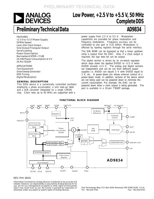
aPreliminary Technical DataFEATURES+2.3 V to +5.5 V Power Supply50 MHz SpeedLow Jitter Clock OutputSine Output/Triangular OutputSerial LoadingPower-Down OptionNarrowband SFDR > 72 dB20 mW Power Consumption at 3 V20-Pin TSSOPAPPLICATIONSTest EquipmentSlow Sweep GeneratorDDS TuningDigital ModulationPRELIMINARY TECHNICAL DATAGENERAL DESCRIPTIONThis DDS device is a numerically controlled oscillatoremploying a phase accumulator, a sine look-up tableand a D/A converter integrated on a single CMOSchip. Clock rates up to 50 MHz are supported with aLow Power, +2.5 V to +5.5 V, 50 MHzComplete DDS<strong>AD9834</strong>power supply from 2.3 V to 5.5 V. Modulationcapabilities are provided for phase modulation andfrequency modulation. Frequency accuracy can becontrolled to one part in 0.25 billion. Modulation iseffected by loading registers through the serial interface.The SIN ROM can be bypassed so that a linear up/downramp is output from the DAC. Also, if a clock output isrequired, the sign data bit can be output.The digital section is driven by an on-board regulatorwhich steps down the applied DVDD to +2.5 V whenDVDD exceeds +2.5 V. The analog and digital sectionsare independent and can be run from different powersupplies i.e. AVDD can equals 5 V with DVDD equal to3 V, etc. A power-down pin allows external control of apower-down mode. In addition, sections of the device whichare not being used can be powered down to minimise thecurrent consumption. For example, the DAC can bepowered down when a clock output is being generated. Thepart is available in a 20-pin TSSOP package.FUNCTIONAL BLOCK DIAGRAMAVDD AGND DGND DVDDCAP/2.5VREFOUTFS ADJUSTMCLKFSELECTRegulatorVCC2.5VOn-BoardReferenceFullScaleControlCOMP28 Bit FREQ0REG28 Bit FREQ1REGMUXPhaseAccumulator(28 Bit)Σ12MSBSINROM10-Bit DACIOUTIOUTB12 Bit PHASE0 REG12 Bit PHASE1 REGMUXDIV BY2MUXMUXCOMPARATORSIGN BIT OUTVIN16 Bit Data RegisterSerial Register16 Bit ControlRegister<strong>AD9834</strong>FSYNCSCLKSDATASLEEPRESETPSELREV PrH 08/01Information furnished by Analog Devices is believed to be accurate andreliable. However, no responsibility is assumed by Analog Devices for itsuse, nor for any infringements of patents or other rights of third partieswhich may result from its use. No license is granted by implication orotherwise under any patent or patent rights of Analog Devices.One Technology Way, P.O. Box 9106, Norwood, MA 02062-9106, U.S.A.Tel: 781/329-4700 Fax: 781/326-8703
<strong>AD9834</strong>PRELIMINARY TECHNICAL DATASPECIFICATIONS 1 (V DD = +2.3 V to +5.5 V; AGND = DGND = 0 V; T A = T MIN to T MAX ; R SET = 6.8 kW ;R LOAD = 200W for IOUT and IOUTB unless otherwise noted)Parameter <strong>AD9834</strong>B Units Test Conditions/CommentsSIGNAL DAC SPECIFICATIONSResolution 10 BitsUpdate Rate (f MAX ) 50 MSPS maxI OUT Full Scale 3.6 mA maxOutput Compliance 2 0.8 V maxDC AccuracyIntegral Nonlinearity ±1 LSB typDifferential Nonlinearity ±0.5 LSB typDDS SPECIFICATIONSDynamic SpecificationsSignal to Noise Ratio 50 dB min f MCLK = , f OUT = f MAX /4096Total Harmonic Distortion -53 dBc max f MCLK = , f OUT = f MAX /4096Spurious Free Dynamic Range (SFDR)Wideband (0 to Nyguist) 50 dBc min f MCLK = f MAX , f OUT = f MCLK /7NarrowBand (± 200 kHz) 72 dBc min f MCLK = f MAX , f OUT = f MCLK /7Clock Feedthrough –55 dBc typWake Up Time 1 ms typPower-Down OptionYesCOMPARATORInput Voltage Range 1 V p-p max ac-coupled internallyInput Capacitance 10 pF typInput HighPass Cutoff Frequency 4 MHz typInput DC Resistance 1 MW typInput DC Current 10 mA maxOutput Rise/Fall Time (15 pF Load) 20 ns typOutput Jitter 100 ps rms typVOLTAGE REFERENCEInternal Reference @ +25°C 1.2 Volts typT MIN to T MAX 1.2 ± 7% Volts min/maxREFIN Input Impedance 3 1 KW typReference TC 100 ppm/°C typLOGIC INPUTSV INH , Input High Voltage DVDD –0.9 V min +3.6 V to +5.5 V Power SupplyDVDD - 0.5 V min +2.7 V to +3.6 V Power Supply2 V min +2.3 V to + 2.7 V Power SupplyV INL , Input Low Voltage 0.9 V max +3.6 V to +5.5 V Power Supply0.5 V max +2.3 V to + 3.6 V Power SupplyI INH , Input Current 1 µA maxC IN , Input Capacitance 10 pF maxPOWER SUPPLIES f OUT = f MCLK /7AVDD 2.3/5.5 V min/V maxDVDD 2.3/5.5 V min/V max4I AA 5 mA max4I DD 1 + 0.04/MHz mA typ4I AA + I DD 7 mA typ 3 V Power Supply10 mA max10 mA typ 5 V Power Supply15 mA maxLow Power Sleep Mode 4 0.25 mA typNOTES1 Operating temperature range is as follows: B Version: –40°C to +85°C.2 Guaranteed by Design.3 Applies when REFIN is sourcing current. The impedance is higher when REFIN is sinking current.4 Measured with the digital inputs static and equal to 0 V or DVDD.Specifications subject to change without notice. There is 95% test coverage of the digital circuitry.–2–REV PrH 08/01
PRELIMINARY TECHNICAL DATA<strong>AD9834</strong>TIMING CHARACTERISTICS (V DD = +2.3 V to +5.5 V; AGND = DGND = 0 V, unless otherwise noted)Limit atT MIN to T MAXParameter (B Version) Units Test Conditions/Commentst 1 20 ns min MCLK Periodt 2 8 ns min MCLK High Durationt 3 8 ns min MCLK Low Durationt 4 25 ns min SCLK Periodt 5 10 ns min SCLK High Durationt 6 10 ns min SCLK Low Durationt 7 5 ns min FSYNC to SCLK Falling Edge Setup Timet 8 10 ns min FSYNC to SCLK Hold TimeSCLK - 5 ns maxt 9 5 ns min Data Setup Timet 10 3 ns min Data Hold Timet 11 8 ns min FSELECT, PSEL0, PSEL1 Setup Time Before MCLK Rising Edge*t 11A 8 ns min FSELECT, PSEL0, PSEL1 Setup Time After MCLK Rising Edge*See Pin Description Section.Guaranteed by design but not production tested.t1MCLKt2t3Figure 1. Master ClockSCLKt 7t 6t 5t 4t 8FSYNCt 9t 10SDATAD15 D14 D2 D1 D0 D15 D14Figure 2. Serial TimingMCLKt 11t 11AFSELECTPSEL0, PSEL1VALID DATA VALID DATA VALID DATAFigure 3. Control TimingREV PrH 08/01–3–
<strong>AD9834</strong>ABSOLUTE MAXIMUM RATINGS*(T A = +25°C unless otherwise noted)PRELIMINARY TECHNICAL DATAAVDD to AGND . . . . . . . . . . . . . . . . . . . . –0.3 V to +7 VDVDD to DGND . . . . . . . . . . . . . . . . . . . . –0.3 V to +7 VAVDD to DVDD . . . . . . . . . . . . . . . . . . –0.3 V to +0.3 VAGND to DGND. . . . . . . . . . . . . . . . . . –0.3 V to +0.3 VDigital I/O Voltage to DGND –0.3 V to DVDD + 0.3 VAnalog I/O Voltage to AGND –0.3 V to AVDD + 0.3 VOperating Temperature RangeIndustrial (B Version) . . . . . . . . . . . . . . –40°C to +85°CStorage Temperature Range . . . . . . . . . –65°C to +150°CMaximum Junction Temperature . . . . . . . . . . . . . +150°CTSSOP q JA Thermal Impedance . . . . . . . . . . . . . 158°C/WLead Temperature, SolderingVapor Phase (60 sec) . . . . . . . . . . . . . . . . . . . . . +215°CInfrared (15 sec) . . . . . . . . . . . . . . . . . . . . . . . . . +220°C*Stresses above those listed under “Absolute Maximum Ratings” may cause permanentdamage to the device. This is a stress rating only and functional operation of the deviceat these or any other conditions above those listed in the operational sections of thisspecification is not implied. Exposure to absolute maximum rating conditions forextended periods may affect device reliability.CAUTIONESD (electrostatic discharge) sensitive device. Electrostatic charges as high as 4000 V readilyaccumulate on the human body and test equipment and can discharge without detection.Although the AD7725 features proprietary ESD protection circuitry, permanent damage mayoccur on devices subjected to high energy electrostatic discharges. Therefore, proper ESDprecautions are recommended to avoid performance degradation or loss of functionality.ORDERING GUIDETemperature Package PackageModel Range Description Option*<strong>AD9834</strong>BRU –40°C to +85°C 20-Pin TSSOP RU-16*RU = Thin Shrink Small Outline Package (TSSOP).FS ADJUSTREFOUTCOMPAVDDDVDDCAP/+2.5VDGNDMCLKFSELPSELPIN CONFIGURATION12345678910<strong>AD9834</strong>OTOP VIEW(Not to Scale)20191817161514131211IOU TBIOUTAGNDVINSIGNBITOUTFSYNCSCLKSDATASLEEPRESETTERMINOLOGYIntegral NonlinearityThis is the maximum deviation of any code from astraight line passing through the endpoints of the transferfunction. The endpoints of the transfer function are zeroscale, a point 0.5 LSB below the first code transition(000 . . . 00 to 000 . . . 01) and full scale, a point 0.5 LSBabove the last code transition (111 . . . 10 to 111 . . . 11).The error is expressed in LSBs.Differential NonlinearityThis is the difference between the measured and ideal 1LSB change between two adjacent codes in the DAC.Output ComplianceThe output compliance refers to the maximum voltagewhich can be generated at the output of the DAC to meetthe specifications. When voltages greater than that specifiedfor the output compliance are generated, the <strong>AD9834</strong>may not meet the specifications listed in the data sheet.Spurious Free Dynamic RangeAlong with the frequency of interest, harmonics of thefundamental frequency and images of the MCLK frequencyare present at the output of a DDS device. Thespurious free dynamic range (SFDR) refers to the largestspur or harmonic which is present in the band of interest.The wide band SFDR gives the magnitude of the largestharmonic or spur relative to the magnitude of the fundamentalfrequency in the 0 to Nyguist bandwidth. Thenarrow band SFDR gives the attenuation of the largest spuror harmonic in a bandwidth of ±200 kHz about the fundamentalfrequency.Clock FeedthroughThere will be feedthrough from the MCLK input to theanalog output. Clock feedthrough refers to the magnitudeof the MCLK signal relative to the fundamental frequencyin the <strong>AD9834</strong>’s output spectrum.–4–REV PrH 08/01
PRELIMINARY TECHNICAL DATAPIN DESCRIPTION<strong>AD9834</strong>Mnemonic FunctionPOWER SUPPLYAVDDAGNDDVDDDGNDCAP/2.5 VPositive power supply for the analog section. A 0.1 µF decoupling capacitor should be connectedbetween AVDD and AGND. AVDD can have a value from +2.3 V to +5.5 V.Analog Ground.Positive power supply for the digital section. A 0.1 µF decoupling capacitor should be connectedbetween DVDD and DGND. DVDD can have a value from +2.3 V to +5.5 V.Digital Ground.The digital circuitry operates from a +2.5 V power supply. This +2.5 V is generated from DVDDusing an on board regulator (when DVDD exceeds +2.5 V). The regulator requires a decouplingcapacitor which is connected from CAP/2.5V to DGND. If DVDD is equal to or less than +2.5 V,CAP/2.5 V should be shorted to DVDD.ANALOG SIGNAL AND REFERENCEIOUT, IOUTB Current Output. This is a high impedance current source. A load resistor should be connectedbetween IOUT and AGND. IOUTB should be tied directly to AGND or through an external loadresistor to AGND.FS ADJUST Full-Scale Adjust Control. A resistor (R SET ) is connected between this pin and AGND. Thisdetermines the magnitude of the full-scale DAC current. The relationship between R SET and the fullscalecurrent is as follows:IOUT FULL-SCALE = 16 x V REFIN /R SETV REFIN = 1.2 V nominal, R SET = 6.8 kW typicalREFOUT Voltage Reference Output. The <strong>AD9834</strong> is used with a 1.23 V reference which is supplied internally.This reference is also made available on the REFOUT pin. It has a value of 1.23 V nominal.COMPCompensation pin. This is a compensation pin for the internal reference amplifier. A 10 nFdecoupling ceramic capacitor should be connected between COMP and AVDD.VINInput to comparator. The comparator can be used to generate a square wave from the sinusoidalDAC output. The DAC output should be filtered appropriately before being applied to thecomparator to improve jitter. When bit SIGNPIB in the control register is set to 1, the comparatorinput is disconnected from VIN. Instead, the NCO's MSB is fed to the comparator input.SIGN BIT OUT Comparator Output. Along with feeding the DAC output into the comparator, the MSB from theNCO can also be output on this pin. When bit SIGNPIB in the control register is set to 1, theNCO's MSB is output. When this bit equals zero, the comparator is connected externally and can beused to convert the DAC's sinusoidal output into a square waveform.DIGITAL INTERFACE AND CONTROLMCLKDigital Clock Input. DDS output frequencies are expressed as a binary fraction of the frequency ofMCLK. The output frequency accuracy and phase noise are determined by this clock.FSELECT Frequency Select Input. FSELECT controls which frequency register, FREQ0 or FREQ1, is usedin the phase accumulator. The frequency register to be used can be selected using the pin FSELECTor the bit FSELECT. FSELECT is sampled on the rising MCLK edge. FSELECT needs to be insteady state when an MCLK rising edge occurs. If FSELECT changes value when a rising edgeoccurs, there is an uncertainty of one MCLK cycle as to when control is transferred to the otherfrequency register. To avoid any uncertainty, a change on FSELECT should not coincide with anMCLK rising edge. When the bit is being used to select the frequency register, the pin FSELECTshould be tied to DGND.PSELPhase Select Input. The <strong>AD9834</strong> has two phase registers. These registers can be used to alter thevalue being input to the SIN ROM. The contents of the phase register can be added to the phaseaccumulator output, the input PSEL selecting the phase register to be used. Like the FSELECTinput, PSEL is sampled on the rising MCLK edge. Therefore, this input needs to be in steady statewhen an MCLK rising edge occurs or there is an uncertainty of one MCLK cycle as to when controlis transferred to the selected phase register. When the phase registers are being controlled by the bitPSEL, the pin should be tied to DGND.SCLKSerial Clock, Logic Input. Data is clocked into the <strong>AD9834</strong> on each falling SCLK edge.SDATASerial Data In, Logic Input. The 16-bit serial data word is applied to this input.FSYNCData Synchronisation Signal, Logic Input. When this input is taken low, the internal logic isinformed that a new word is being loaded into the device.RESETRESET, active high digital input. RESET resets the phase accumulator to zero which corresponds toREV PrH 08/01–5–
<strong>AD9834</strong>SLEEPPRELIMINARY TECHNICAL DATAan anlog output of midscale.Low Power Control, active high digital input. SLEEP puts the <strong>AD9834</strong> into a low power mode.Internal clocks are disabled and the DAC's current sources are turned off. The <strong>AD9834</strong> is re-enabledby taking SLEEP low.Table I. Frequency/Phase RegistersRegister Size DescriptionFREQ0 REG 28 Bits Frequency Register 0. This definesthe output frequency,when FSELECT = 0, as a fractionof the MCLK frequency.FREQ1 REG 28 Bits Frequency Register 1. This definesthe output frequency,when FSELECT = 1, as a fractionof the MCLK frequency.PHASE0 REG 12 Bits Phase Offset Register 0. WhenPSEL = 0, the contents of thisregister are added to the outputof the phase accumulator.PHASE1 REG 12 Bits Phase Offset Register 1. WhenPSEL = 1, the contents of thisregister are added to the outputof the phase accumulator.Table 2. Frequency Register BitsD15 D14 D13D00 1 MSB 14 FREQ0 REG BITS LSB1 0 MSB 14 FREQ1 REG BITS LSBTable 3. Phase Register BitsD15 D14 D13 D12 D11D01 1 0 X MSB 12 PHASE0 REG BITS LSB1 1 1 X MSB 12 PHASE1 REG BITS LSBTable 4. Control RegisterD15 D14 D130 0 CONTROL BITSD0Table 5. Control Register BitsBit Name FunctionD13 B28 Two write operations are required toload a new word into the FREQ registers.When the complete register isbeing loaded with a new 28-bit word,B28 can be set to 1. The first write toaddress 01 or 10 contains the 14 LSBsof the frequency word. The next writeto this address will contain the 14MSBs. When B28 is set to 0, the frequencyregister operates as 2 registers,one containing the 14 MSBs and theother containing the 14 LSBs. To alterthe 14 MSBs or the 14 LSBs, asingle write is made to the FREQ addresswhile D12 of the control registerinforms the <strong>AD9834</strong> whether the bitsare MSBs or LSBs.D12 HLB When B28 is set to 0, the 14 MSBs ofthe frequency word can be altered independentof the 14 LSBs and viceversa. A single write is made to theappropriate frequency address whilethe HLB bit indicates whether the 14bits being loaded are being transferredto the 14 MSBs or 14 LSBs of the register.This allows the user to continuouslyload the MSBs or LSBs whileignoring the remaining 14 bits. Thisis useful if the complete 28 bit resolutionis not required. When HLBequals 1, the 14 bits of data are transferredinto the 14 MSBs of the frequencyregister. When HLB equals 0,the 14 LSBs of the frequency registerare loaded.D11 FSELECT This is the FSELECT bit.D10 PSEL This is the PSEL bit.D9 PIN/SW The RESET, FSELECT, PSEL andSLEEP functions can be controlled viabits in the control register or pins.PIN/SW selects the source of controlfor these functions. When this bitequals 0, the PHASE/FREQ registersare selected using the bits FSELECTand PSEL. The device can be resetusing the RESET bit and the part ispowered down using the SLEEP12 bit.When PIN/SW equals 1, the registersare selected using the FSELECT andPSEL pins. The RESET pin is used–6–REV PrH 08/01
PRELIMINARY TECHNICAL DATAto reset the phase accumulator whilethe device is powered down using theSLEEP pin.D8 RESET This bit resets the phase accumulatorto zero which corresponds to an analogoutput of midscale. The bit is set to 1to perform a reset. The accumulatorwill remain in the reset condition untilRESET is set to 0.D7 SLEEP1 When this bit is set to 1, the internalclock is disabled. The DAC outputwill remain at its present value as theNCO is no longer accumulating.D6 SLEEP12 When this bit equals 1, the DAC ispowered down. This is useful whenthe <strong>AD9834</strong> is used to output theNCO's MSB only. In this case, theDAC is not required so, it can bepowered down to reduce the powerconsumption.D5 OPBITEN When this bit is set to 1, the MSBfrom the phase accumulator is routedto pin SIGN BIT OUT. It can besent directly to the pin or, it can be dividedby 2 prior to being output. BitPIHB determines whether the squarewave generated by the MSB is dividedby 2 before being output. WhenOPBITEN equals 0, there is no outputat SIGN BIT OUT.<strong>AD9834</strong>D4 SIGNPIB When this bit is set to 0, the MSBfrom the phase accumulator isconnected to pin SIGN BIT OUT, thesquare wave being divided by one ordivided by two before being output.Bit PIHB determines the frequency ofthe square wave. When SIGNPIBequals 1, the on board comparator isconnected to SIGN BIT OUT. Afterfiltering the sinusoidal output from theDAC appropriately, the waveform canbe applied to the comparator togenerate a square waveform.D3 PIHB This bit is used in association withOPBITEN. When OPBITEN equals1, the MSB is output on pin SIGNBIT OUT to generate a square wave.When PIHB equals 0, the square waveis divided by 2 before being output.When PIHB equals 1, the MSB ispassed directly to the output.D2 Reserved This bit must be set to 0.D1 MODE When MODE is set to 0 with SLEEP1equal to zero, the ROM is used toconvert the phase information intoamplitude information which results ina sinusoidal signal at the output.When MODE is set to 1 and SLEEP1is set to 0, the ROM is bypassed andthe phase information from the phaseaccumulator is sent directly to theDAC which results in a ramp output.D0 Reserved This bit must be set to 0.SLEEP12SLEEP1RESETPhaseAccumulator(28 Bit)SINROM0MUX1(Low Power)10-Bit DAC<strong>AD9834</strong>IOUTIOUTBMODE + SLEEP1COMPARATORVINSIGN/PIPIHB1MUX0DIV BY21MUX0DIGITALOUTPUT(enable)SIGN BIT OUTOPBITENDB15 DB14 DB13 DB12 DB11 DB10 DB9 DB8 DB7 DB6 DB5 DB4 DB3 DB2 DB1 DB0ADDRS B28 HLB FSEL PSEL PIN/SW RESET SLEEP1 SLEEP12 OPBITEN SIGN/PI PIHB 0 MODE 0Figure 4. Function of Control BitsREV PrH 08/01–7–
<strong>AD9834</strong>PRELIMINARY TECHNICAL DATACIRCUIT DESCRIPTIONThe <strong>AD9834</strong> combines the Numerical ControlledOscillator (NCO), SINE Look- Up Table, Frequency andPhase Modulators, and a Digital-to- Analog Converter ona single integrated circuit.The internal circuitry of the <strong>AD9834</strong> consists of threemain sections. These are:Numerical Controlled Oscillator (NCO) + PhaseModulatorSINE Look-Up TableDigital-to-Analog ConverterThe <strong>AD9834</strong> is a fully integrated Direct Digital Synthesis(DDS) chip. The chip requires one reference clock, onelow precision resistor and eight decoupling capacitors toprovide digitally created sine waves up to 25 MHz. Inaddition to the generation of this RF signal, the chip isfully capable of a broad range of simple and complexmodulation schemes. These modulation schemes arefully implemented in the digital domain allowing accurateand simple realization of complex modulation algorithmsusing DSP techniques.THEORY OF OPERATIONSine waves are typically thought of in terms of theirmagnitude form a(t) = sin (wt). However, these arenonlinear and not easy to generate except through piecewise construction. On the other hand, the angularinformation is linear in nature. That is, the phase anglerotates through a fixed angle for each unit of time. Theangular rate depends on the frequency of the signal by thetraditional rate of w = 2pf.+10—12π0MAGNITUDEPHASEFigure 7. Sine WaveKnowing that the phase of a sine wave is linear and given areference interval (clock period), the phase rotation forthat period can be determined.DPhase = wdtSolving for ww = DPhase/dt = 2pfSolving for f and substituting the reference clock frequencyfor the reference period (1/f MCLK = dt)f = DPhase x f MCLK /2pThe <strong>AD9834</strong> builds the output based on this simpleequation. A simple DDS chip can implement thisequation with three major subcircuits.Numerical Controlled Oscillator + Phase ModulatorThis consists of two frequency select registers, a phaseaccumulator and two phase offset registers. The maincomponent of the NCO is a 28-bit phase accumulatorwhich assembles the phase component of the outputsignal. Continuous time signals have a phase range of 0to 2p. Outside this range of numbers, the sinusoidfunctions repeat themselves in a periodic manner. Thedigital implementation is no different. The accumulatorsimply scales the range of phase numbers into a multibitdigital word. The phase accumulator in the <strong>AD9834</strong> isimplemented with 28 bits. Therefore, in the <strong>AD9834</strong>, 2p= 2 28 . Likewise, the DPhase term is scaled into this rangeof numbers 0 < DPhase < 2 28 – 1. Making thesesubstitutions into the equation abovef = DPhase x f MCLK /2 28where 0 < DPhase < 2 28The input to the phase accumulator (i.e., the phase step)can be selected either from the FREQ0 Register orFREQ1 Register and this is controlled by the FSELECTpin or the FSELECT bit. NCOs inherently generatecontinuous phase signals, thus avoiding any outputdiscontinuity when switching between frequencies.Following the NCO, a phase offset can be added toperform phase modulation using the 12-bit PHASERegisters. The contents of this register are added to themost significant bits of the NCO. The <strong>AD9834</strong> has twoPHASE registers, the resolution of these registers being2p/4096.Sine Look-Up Table (LUT)To make the output useful, the signal must be convertedfrom phase information into a sinusoidal value. Sincephase information maps directly into amplitude, a ROMLUT converts the phase information into amplitude. Todo this, the digital phase information is used to address asine ROM LUT. Although the NCO contains a 28-bitphase accumulator, the output of the NCO is truncated to12 bits. Using the full resolution of the phaseaccumulator is impractical and unnecessary as this wouldrequire a look-up table of 2 28 entries.It is necessary only to have sufficient phase resolution inthe LUTs such that the dc error of the output waveform isdominated by the quantization error in the DAC. Thisrequires the look-up table to have two bits of phaseresolution more than the 10-bit DAC.The SINE look up table is enabled using bits MODE andSLEEP1 in the control register. To enable the ROM,MODE is set to 0 and SLEEP1 is set to 1.Ramp OutputThe SINE look up table can be bypassed so that thetruncated digital output from the NCO is sent to theDAC. In this case, the output is no longer sinusoidal.The DAC will produce a ramp up/down function. TheMODE bit in the control register determines whether theSINE ROM is used or bypassed. When MODE equals 1and SLEEP1 is set to 0, the ROM is bypassed.Digital-to-Analog ConverterThe <strong>AD9834</strong> includes a high impedance current source10-bit DAC, capable of driving a wide range of loads at–8–REV PrH 08/01
PRELIMINARY TECHNICAL DATAdifferent speeds. Full-scale output current can be adjusted,for optimum power and external load requirements,through the use of a single external resistor (R SET ).The DAC is configured for single ended operation. Theload resistor can be any value required, as long as the fullscalevoltage developed across it does not exceed thevoltage compliance range. Since full-scale current iscontrolled by R SET , adjustments to R SET can balancechanges made to the load resistor. However, if the DACfull-scale output current is significantly less than 0.5 mA,the DAC’s linearity may degrade.ComparatorWhen the <strong>AD9834</strong> is used to generate clock sources, theon board comparator can be used to convert the DAC'ssinusoidal signal to a square wave. The output from theDAC may be filtered externally before being applied tothe comparator input. The comparator's input is accoupled.It can accept a fullscale signal of 1 Vpp whichhas a frequency in excess of 4 MHz. The comparator'soutput will be a square wave with an amplitude from 0 Vto DVDD.To enable the comparator, bit SIGNPIB is set to 0.MSB from the NCOThe MSB from the NCO can also be output from the<strong>AD9834</strong>. By setting the SIGNPIB to one, the MSB fromthe NCO is supplied to the comparator. This is useful asa coarse clock source.RegulatorThe digital section of the device is operated at 2.5 V. Anon board regulator steps down DVDD to 2.5 V. Thedigital inteface (serial port) is operated with a supply ofDVDD. The digital signals are level shifted within the<strong>AD9834</strong> to make them 2.5V compatible.When the digital section is operated with a supply of 2.5V(DVDD = 2.5V), pins CAP/2.5V and DVDD should betied together.The analog section can be operated with a power supplyfrom 2.5V to 5.5V also. AVDD is set independent ofDVDD i.e. the analog section can be operated at 5V andthe digital section can be operated at 3V or vice versa.DSP and MPU InterfacingThe <strong>AD9834</strong> has a serial interface, with 16 bits beingloaded during each write cycle. SCLK, SDATA andFSYNC are used to load the word into the <strong>AD9834</strong>.When FSYNC is taken low, the <strong>AD9834</strong> is informed thata word is being written to the device. The first bit is readinto the device on the next SCLK falling edge with theremaining bits being read into the device on the subsequentSCLK falling edges. FSYNC frames the 16 bits,therefore, when 16 SCLK falling edges have occurred,FSYNC should be taken high again. The SCLK can becontinuous or, alternatively, the SCLK can idle high orlow between write operations.When writing to a frequency register, bits D15 and D14give the address of the frequency register. To alter theentire contents of a frequency register, B28 should be setto 1. In this mode, two consecutive writes to the same<strong>AD9834</strong>address can be performed, the first write containing the 14LSBs while the second write contains the 14 MSBs.In some applications, the user does not need to alter all 28bits of the frequency register. With coarse tuning, onlythe 14 MSBs are altered while with fine tuning, only the14 LSBs are altered. By setting bit B28 to zero, the 14LSBs or MSBs can be altered independently i.a. all 28bits do not have to be written to the <strong>AD9834</strong>. Bit HLB inthe control register identifies which 14 bits are being altered.For example, to alter the 14 MSBs of frequencyregister 0, HLB is set to one. A single write to address 01will load the 14 data bits in the 16-bit word to the 14MSBs of FREQ REG 0.When writing to a phase register, bits D15 and D14 areset to 11. Bits D13 and D12 identify which phase registeris being loaded.The phase and frequency registers to be used are selectedusing the pins FSELECT and PSEL or the correspondingbits can be used. Bit PIN/SW determines whether the bitsor the pins are used. When PIN/SW = 1, the pins areused while the bits are used when PIN/SW = 0.Associated with each operation is a latency. When inputsFSELECT/PSEL change value, there will be a pipelinedelay before control is transferred to the selectedregister—there will be a pipeline delay before the analogoutput is controlled by the selected register. When timest11 and t11A are met, PSEL and FSELECT havelatencies of six MCLK cycles. When times t11 and t11Aare not met, the latency can increase by one MCLK cycle.Similarly, there is a latency associated with each writeoperation. If a selected frequency/phase register is loadedwith a new word, there is a delay of 6 to 7 MCLK cyclesbefore the analog output will change (there is anuncertainty of one MCLK cycle regarding the MCLKrising edge at which the data is loaded into the destinationregister).The flow chart in Figure X shows the operating routinefor the <strong>AD9834</strong>. When the <strong>AD9834</strong> is powered up, thepart should be reset. This will reset the phaseaccumulator to zero so that the analog output is atmidscale. To avoid spurious DAC outputs while the<strong>AD9834</strong> is being initialized, the RESET bit/pin should beset to 1 until the part is ready to begin generating anoutput. RESET does not reset the phase and frequencyregisters. These registers will contain invalid data and,therefore, should be set to a known value by the user.The RESET bit/pin is then set to 0 to begin generating anoutput. A signal will appear at the DAC output 6 MCLKcycles after RESET is set to 0.The analog output is f MCLK /2 28 x FREG where FREG is thevalue loaded into the selected frequency register. Thissignal will be phase shifted by the amount specified in theselected phase register (2p/4096 x PHASEREG wherePHASEREG is the value contained in the selected phaseregister).Control of the frequency/phase registers can beinterchanged from the pins to the bits.REV PrH 08/01–9–
<strong>AD9834</strong>PRELIMINARY TECHNICAL DATAAPPLICATIONSThe <strong>AD9834</strong> contains functions which make it suitable formodulation applications. The part can be used to performsimple modulation such as FSK. More complexmodulation schemes such as GMSK and QPSK can alsobe implemented using the <strong>AD9834</strong>. In an FSKapplication, the two frequency registers of the <strong>AD9834</strong> areloaded with different values; one frequency will representthe space frequency while the other will represent themark frequency. The digital data stream is fed to theFSELECT pin which will cause the <strong>AD9834</strong> to modulatethe carrier frequency between the two values.The <strong>AD9834</strong> has two phase registers; this enables the partto perform PSK. With phase shift keying, the carrierfrequency is phase shifted, the phase being altered by anamount which is related to the bit stream being input tothe modulator. The presence of four shift registers easesthe interaction needed between the DSP and the <strong>AD9834</strong>.The <strong>AD9834</strong> is also suitable for signal generatorapplications. With its low current consumption, the partis suitable for applications in which it can be used as alocal oscillator.Grounding and LayoutThe printed circuit board that houses the <strong>AD9834</strong> shouldbe designed so that the analog and digital sections areseparated and confined to certain areas of the board. Thisfacilitates the use of ground planes which can be separatedeasily. A minimum etch technique is generally best forground planes as it gives the best shielding. Digital andanalog ground planes should only be joined in one place.If the <strong>AD9834</strong> is the only device requiring an AGND toDGND connection, then the ground planes should beconnected at the AGND and DGND pins of the <strong>AD9834</strong>.If the <strong>AD9834</strong> is in a system where multiple devicesrequire AGND to DGND connections, the connectionshould be made at one point only, a star ground point thatshould be established as close as possible to the <strong>AD9834</strong>.Avoid running digital lines under the device as these willcouple noise onto the die. The analog ground planeshould be allowed to run under the <strong>AD9834</strong> to avoid noisecoupling. The power supply lines to the <strong>AD9834</strong> shoulduse as large a track as is possible to provide lowimpedance paths and reduce the effects of glitches on thepower supply line. Fast switching signals such as clocksshould be shielded with digital ground to avoid radiatingnoise to other sections of the board. Avoid crossover ofdigital and analog signals. Traces on opposite sides of theboard should run at right angles to each other. This willreduce the effects of feedthrough through the board. Amicrostrip technique is by far the best but is not alwayspossible with a double-sided board. In this technique, thecomponent side of the board is dedicated to ground planeswhile signals are placed on the other side.Good decoupling is important. The analog and digitalsupplies to the <strong>AD9834</strong> are independent and separatelypinned out to minimize coupling between analog anddigital sections of the device. All analog and digitalsupplies should be decoupled to AGND and DGNDrespectively with 0.1 µF ceramic capacitors in parallelwith 10 µF tantalum capacitors. To achieve the best fromthe decoupling capacitors, they should be placed as closeas possible to the device, ideally right up against thedevice. In systems where a common supply is used todrive both the AVDD and DVDD of the <strong>AD9834</strong>, it isrecommended that the system’s AVDD supply be used.This supply should have the recommended analog supplydecoupling between the AVDD pins of the <strong>AD9834</strong> andAGND and the recommended digital supply decouplingcapacitors between the DVDD pins and DGND.Interfacing the <strong>AD9834</strong> to MicroprocessorsThe <strong>AD9834</strong> has a standard serial interface which allowsthe part to interface directly with several microprocessors.The device uses an external serial clock to write the data/control information into the device. The serial clock canhave a frequency of 20 MHz maximum. The serial clockcan be continuous or, it can idle high or low betweenwrite operations. When data/control information is beingwritten to the <strong>AD9834</strong>, FSYNC is taken low and is heldlow while the 16 bits of data are being written into the<strong>AD9834</strong>. The FSYNC signal frames the 16 bits of informationbeing loaded into the <strong>AD9834</strong>.<strong>AD9834</strong> to ADSP-21xx InterfaceFigure 12 shows the serial interface between the <strong>AD9834</strong>and the ADSP-21xx. The ADSP-21xx should be set upto operate in the SPORT Transmit Alternate FramingMode (TFSW = 1). The ADSP-21xx is programmedthrough the SPORT control register and should be configuredas follows: Internal clock operation (ISCLK = 1),Active low framing (INVTFS = 1), 16-bit word length(SLEN = 15), Internal frame sync signal (ITFS = 1),Generate a frame sync for each write operation (TFSR =1). Transmission is initiated by writing a word to the Txregister after the SPORT has been enabled. The data isclocked out on each rising edge of the serial clock andclocked into the <strong>AD9834</strong> on the SCLK falling edge.ADSP2101/ADSP2103TFSDTSCLKADDITIONAL PINS OMITTED FOR CLARITYFSYNCSDATASCLK<strong>AD9834</strong>Figure 12. ADSP2101/ADSP2103 to <strong>AD9834</strong> Interface<strong>AD9834</strong> to 68HC11/68L11 InterfaceFigure 13 shows the serial interface between the <strong>AD9834</strong>and the 68HC11/68L11 microcontroller. Themicrocontroller is configured as the master by setting bitMSTR in the SPCR to 1 and, this provides a serial clockon SCK while the MOSI output drives the serial data lineSDATA. Since the microcontroller does not have a dedi-–10–REV PrH 08/01
PRELIMINARY TECHNICAL DATAcated frame sync pin, the FSYNC signal is derived from aport line (PC7). The set up conditions for correct operationof the interface are as follows: the SCK idles highbetween write operations (CPOL = 0), data is valid on theSCK falling edge (CPHA = 1). When data is being transmittedto the <strong>AD9834</strong>, the FSYNC line is taken low(PC7). Serial data from the 68HC11/68L11 is transmittedin 8-bit bytes with only 8 falling clock edges occuringin the transmit cycle. Data is transmitted MSB first. Inorder to load data into the <strong>AD9834</strong>, PC7 is held low afterthe first 8 bits are transferred and a second serial writeoperation is performed to the <strong>AD9834</strong>. Only after thesecond 8 bits have been transferred should FSYNC betaken high again.68HC11/68L11PC7MOSISCKADDITIONAL PINS OMITTED FOR CLARITYFSYNCSDATASCLK<strong>AD9834</strong>80C51/80L51P3.3RXDTXDADDITIONAL PINS OMITTED FOR CLARITYFSYNCSDATASCLK<strong>AD9834</strong>Figure 14. 80C51/80L51 to <strong>AD9834</strong> Interface<strong>AD9834</strong><strong>AD9834</strong> to DSP56002 InterfaceFigure 15 shows the interface between the <strong>AD9834</strong> andthe DSP56002. The DSP56002 is configured for normalmode asynchronous operation with a Gated internal clock(SYN = 0, GCK = 1, SCKD = 1). The frame sync pin isgenerated internally (SC2 = 1), the transfers are 16 bitswide (WL1 = 1, WL0 = 0) and the frame sync signal willframe the 16 bits (FSL = 0). The frame sync signal isavailable on pin SC2 but, it needs to be inverted beforebeing applied to the <strong>AD9834</strong>. The interface to theDSP56000/DSP56001 is similar to that of the DSP56002.Figure 13. 68HC11/68L11 to <strong>AD9834</strong> Interface<strong>AD9834</strong> to 80C51/80L51 InterfaceFigure 14 shows the serial interface between the <strong>AD9834</strong>and the 80C51/80L51 microcontroller. Themicrocontroller is operated in mode 0 so that TXD of the80C51/80L51 drives SCLK of the <strong>AD9834</strong> while RXDdrives the serial data line SDATA. The FSYNC signal isagain derived from a bit programmable pin on the port(P3.3 being used in the diagram). When data is to betransmitted to the <strong>AD9834</strong>, P3.3 is taken low. The80C51/80L51 transmits data in 8 bit bytes thus, only 8falling SCLK edges occur in each cycle. To load theremaining 8 bits to the <strong>AD9834</strong>, P3.3 is held low after thefirst 8 bits have been transmitted and a second write operationis initiated to transmit the second byte of data.P3.3 is taken high following the completion of the secondwrite operation. SCLK should idle high between the twowrite operations. The 80C51/80L51 outputs the serialdata in a format which has the LSB first. The <strong>AD9834</strong>accepts the MSB first (the 4 MSBs being the control information,the next 4 bits being the address while the 8LSBs contain the data when writing to a destination register).Therefore, the transmit routine of the 80C51/80L51must take this into account and re-arrange the bits so thatthe MSB is output first.DSP56002<strong>AD9834</strong>SC2FSYNCSTDSDATASCKSCLKADDITIONAL PINS OMITTED FOR CLARITYFigure 15. <strong>AD9834</strong> to DSP56002 InterfaceREV PrH 08/01–11–