
You also want an ePaper? Increase the reach of your titles
YUMPU automatically turns print PDFs into web optimized ePapers that Google loves.
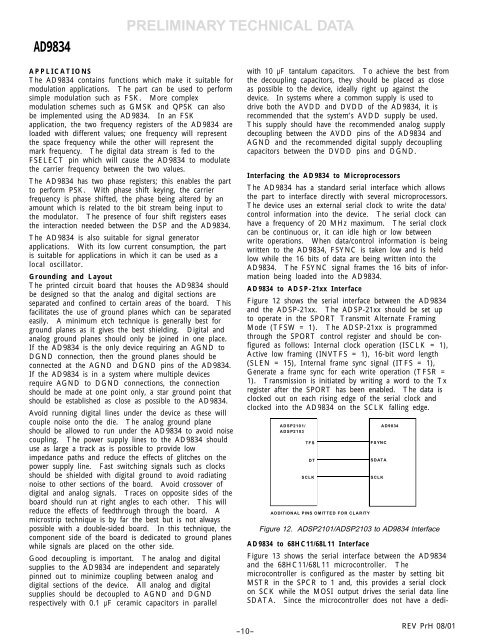
<strong>AD9834</strong>PRELIMINARY TECHNICAL DATAAPPLICATIONSThe <strong>AD9834</strong> contains functions which make it suitable formodulation applications. The part can be used to performsimple modulation such as FSK. More complexmodulation schemes such as GMSK and QPSK can alsobe implemented using the <strong>AD9834</strong>. In an FSKapplication, the two frequency registers of the <strong>AD9834</strong> areloaded with different values; one frequency will representthe space frequency while the other will represent themark frequency. The digital data stream is fed to theFSELECT pin which will cause the <strong>AD9834</strong> to modulatethe carrier frequency between the two values.The <strong>AD9834</strong> has two phase registers; this enables the partto perform PSK. With phase shift keying, the carrierfrequency is phase shifted, the phase being altered by anamount which is related to the bit stream being input tothe modulator. The presence of four shift registers easesthe interaction needed between the DSP and the <strong>AD9834</strong>.The <strong>AD9834</strong> is also suitable for signal generatorapplications. With its low current consumption, the partis suitable for applications in which it can be used as alocal oscillator.Grounding and LayoutThe printed circuit board that houses the <strong>AD9834</strong> shouldbe designed so that the analog and digital sections areseparated and confined to certain areas of the board. Thisfacilitates the use of ground planes which can be separatedeasily. A minimum etch technique is generally best forground planes as it gives the best shielding. Digital andanalog ground planes should only be joined in one place.If the <strong>AD9834</strong> is the only device requiring an AGND toDGND connection, then the ground planes should beconnected at the AGND and DGND pins of the <strong>AD9834</strong>.If the <strong>AD9834</strong> is in a system where multiple devicesrequire AGND to DGND connections, the connectionshould be made at one point only, a star ground point thatshould be established as close as possible to the <strong>AD9834</strong>.Avoid running digital lines under the device as these willcouple noise onto the die. The analog ground planeshould be allowed to run under the <strong>AD9834</strong> to avoid noisecoupling. The power supply lines to the <strong>AD9834</strong> shoulduse as large a track as is possible to provide lowimpedance paths and reduce the effects of glitches on thepower supply line. Fast switching signals such as clocksshould be shielded with digital ground to avoid radiatingnoise to other sections of the board. Avoid crossover ofdigital and analog signals. Traces on opposite sides of theboard should run at right angles to each other. This willreduce the effects of feedthrough through the board. Amicrostrip technique is by far the best but is not alwayspossible with a double-sided board. In this technique, thecomponent side of the board is dedicated to ground planeswhile signals are placed on the other side.Good decoupling is important. The analog and digitalsupplies to the <strong>AD9834</strong> are independent and separatelypinned out to minimize coupling between analog anddigital sections of the device. All analog and digitalsupplies should be decoupled to AGND and DGNDrespectively with 0.1 µF ceramic capacitors in parallelwith 10 µF tantalum capacitors. To achieve the best fromthe decoupling capacitors, they should be placed as closeas possible to the device, ideally right up against thedevice. In systems where a common supply is used todrive both the AVDD and DVDD of the <strong>AD9834</strong>, it isrecommended that the system’s AVDD supply be used.This supply should have the recommended analog supplydecoupling between the AVDD pins of the <strong>AD9834</strong> andAGND and the recommended digital supply decouplingcapacitors between the DVDD pins and DGND.Interfacing the <strong>AD9834</strong> to MicroprocessorsThe <strong>AD9834</strong> has a standard serial interface which allowsthe part to interface directly with several microprocessors.The device uses an external serial clock to write the data/control information into the device. The serial clock canhave a frequency of 20 MHz maximum. The serial clockcan be continuous or, it can idle high or low betweenwrite operations. When data/control information is beingwritten to the <strong>AD9834</strong>, FSYNC is taken low and is heldlow while the 16 bits of data are being written into the<strong>AD9834</strong>. The FSYNC signal frames the 16 bits of informationbeing loaded into the <strong>AD9834</strong>.<strong>AD9834</strong> to ADSP-21xx InterfaceFigure 12 shows the serial interface between the <strong>AD9834</strong>and the ADSP-21xx. The ADSP-21xx should be set upto operate in the SPORT Transmit Alternate FramingMode (TFSW = 1). The ADSP-21xx is programmedthrough the SPORT control register and should be configuredas follows: Internal clock operation (ISCLK = 1),Active low framing (INVTFS = 1), 16-bit word length(SLEN = 15), Internal frame sync signal (ITFS = 1),Generate a frame sync for each write operation (TFSR =1). Transmission is initiated by writing a word to the Txregister after the SPORT has been enabled. The data isclocked out on each rising edge of the serial clock andclocked into the <strong>AD9834</strong> on the SCLK falling edge.ADSP2101/ADSP2103TFSDTSCLKADDITIONAL PINS OMITTED FOR CLARITYFSYNCSDATASCLK<strong>AD9834</strong>Figure 12. ADSP2101/ADSP2103 to <strong>AD9834</strong> Interface<strong>AD9834</strong> to 68HC11/68L11 InterfaceFigure 13 shows the serial interface between the <strong>AD9834</strong>and the 68HC11/68L11 microcontroller. Themicrocontroller is configured as the master by setting bitMSTR in the SPCR to 1 and, this provides a serial clockon SCK while the MOSI output drives the serial data lineSDATA. Since the microcontroller does not have a dedi-–10–REV PrH 08/01