
Create successful ePaper yourself
Turn your PDF publications into a flip-book with our unique Google optimized e-Paper software.
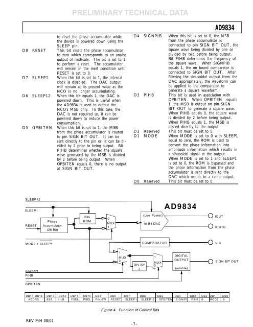
PRELIMINARY TECHNICAL DATAto reset the phase accumulator whilethe device is powered down using theSLEEP pin.D8 RESET This bit resets the phase accumulatorto zero which corresponds to an analogoutput of midscale. The bit is set to 1to perform a reset. The accumulatorwill remain in the reset condition untilRESET is set to 0.D7 SLEEP1 When this bit is set to 1, the internalclock is disabled. The DAC outputwill remain at its present value as theNCO is no longer accumulating.D6 SLEEP12 When this bit equals 1, the DAC ispowered down. This is useful whenthe <strong>AD9834</strong> is used to output theNCO's MSB only. In this case, theDAC is not required so, it can bepowered down to reduce the powerconsumption.D5 OPBITEN When this bit is set to 1, the MSBfrom the phase accumulator is routedto pin SIGN BIT OUT. It can besent directly to the pin or, it can be dividedby 2 prior to being output. BitPIHB determines whether the squarewave generated by the MSB is dividedby 2 before being output. WhenOPBITEN equals 0, there is no outputat SIGN BIT OUT.<strong>AD9834</strong>D4 SIGNPIB When this bit is set to 0, the MSBfrom the phase accumulator isconnected to pin SIGN BIT OUT, thesquare wave being divided by one ordivided by two before being output.Bit PIHB determines the frequency ofthe square wave. When SIGNPIBequals 1, the on board comparator isconnected to SIGN BIT OUT. Afterfiltering the sinusoidal output from theDAC appropriately, the waveform canbe applied to the comparator togenerate a square waveform.D3 PIHB This bit is used in association withOPBITEN. When OPBITEN equals1, the MSB is output on pin SIGNBIT OUT to generate a square wave.When PIHB equals 0, the square waveis divided by 2 before being output.When PIHB equals 1, the MSB ispassed directly to the output.D2 Reserved This bit must be set to 0.D1 MODE When MODE is set to 0 with SLEEP1equal to zero, the ROM is used toconvert the phase information intoamplitude information which results ina sinusoidal signal at the output.When MODE is set to 1 and SLEEP1is set to 0, the ROM is bypassed andthe phase information from the phaseaccumulator is sent directly to theDAC which results in a ramp output.D0 Reserved This bit must be set to 0.SLEEP12SLEEP1RESETPhaseAccumulator(28 Bit)SINROM0MUX1(Low Power)10-Bit DAC<strong>AD9834</strong>IOUTIOUTBMODE + SLEEP1COMPARATORVINSIGN/PIPIHB1MUX0DIV BY21MUX0DIGITALOUTPUT(enable)SIGN BIT OUTOPBITENDB15 DB14 DB13 DB12 DB11 DB10 DB9 DB8 DB7 DB6 DB5 DB4 DB3 DB2 DB1 DB0ADDRS B28 HLB FSEL PSEL PIN/SW RESET SLEEP1 SLEEP12 OPBITEN SIGN/PI PIHB 0 MODE 0Figure 4. Function of Control BitsREV PrH 08/01–7–