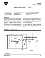
TDA3566A PAL/NTSC decoder
TDA3566A PAL/NTSC decoder
TDA3566A PAL/NTSC decoder

Create successful ePaper yourself
Turn your PDF publications into a flip-book with our unique Google optimized e-Paper software.
Philips SemiconductorsProduct specification<strong>PAL</strong>/<strong>NTSC</strong> <strong>decoder</strong><strong>TDA3566A</strong>The time constant of the saturationcontrol (pin 5) provides a delayedswitch-on after killing. Adjustment ofthe oscillator is achieved by variationof the burst phase detector loadresistance between pins 24 and 25(see Fig.8).With this application the trimmercapacitor in series with the 8.8 MHzcrystal (pin 26) can be replaced by afixed value capacitor to compensatefor unbalance of the phase detector.DemodulatorThe (R−Y) and (B−Y) demodulatorsare driven by the colour differencesignals from the delay-line matrixcircuit and the reference signals fromthe 8.8 MHz divider circuit. The (R−Y)reference signal is fed via the<strong>PAL</strong>-switch. The output signals arefed to the R and B matrix circuits andto the (G−Y) matrix to provide the(G−Y) signal which is applied to theG-matrix. The demodulation circuitsare killed and blanked by by-passingthe input signals.<strong>NTSC</strong> modeThe <strong>NTSC</strong> mode is switched on whenthe voltage at the burst phasedetector outputs (pins 24 and 25) isadjusted below 9 V.To ensure reliable application thephase detector load resistors areexternal. When the <strong>TDA3566A</strong> isused only for <strong>PAL</strong> these two 33 kΩresistors must be connected to +12 V(see Fig.8).For <strong>PAL</strong>/<strong>NTSC</strong> application the valueof each resistor must be reduced to20 kΩ (with a tolerance of 1%) andconnected to the slider of apotentiometer (see Fig.9). Theswitching transistor brings the voltageat pins 24 and 25 below 9 V whichswitches the circuit tot the <strong>NTSC</strong>mode.The position of the <strong>PAL</strong> flip-flopensures that the correct phase of the(R−Y) reference signal is supplied tothe (R−Y) demodulator.The drive to the H/2 detector is nowprovided by the (B−Y) referencesignal. In the <strong>PAL</strong> mode it is driven bythe (R−Y) reference signal. Huecontrol is realized by changing thephase of the reference drive to theburst phase detector.This is achieved by varying thevoltage at pins 24 and 25 between7.0 V and 8.5 V, nominal position7.65 V. The hue control characteristicis shown in Fig.6.RGB matrix and amplifiersThe three matrix and amplifier circuitsare identical and only one circuit willbe described.The luminance and the colourdifference signals are added in thematrix circuit to obtain the coloursignal, which is then fed to thecontrast control stage.The contrast control voltage issupplied to pin 6 (high-inputimpedance). The control range is+5 dB to −11.5 dB nominal. Therelationship between the controlvoltage and the gain is linear (seeFig.3).During the 3-line period after blankinga pulse is inserted at the output of thecontrast control stage. The amplitudeof this pulse is varied by a controlvoltage at pin 11. This applies avariable offset to the normal blacklevel, thus providing brightnesscontrol.The brightness control range is 1 V to3.6 V. While this offset level ispresent, the black-current inputimpedance (pin 18) is high and theinternal clamp circuit is activated. Theclamp circuit then compares thereference voltage at pin 19 with thevoltage developed across theexternal resistor network R A andR B (pin 18) which is provided bypicture tube beam current.The output of the comparator isstored in capacitors connected frompins 10, 20 and 21 to ground whichcontrols the black level at the output.The reference voltage is composedby the resistor divider network and theleakage current of the picture tubeinto this bleeder. During verticalblanking, this voltage is stored in thecapacitor connected to pin 19, whichensures that the leakage current ofthe CRT does not influence the blackcurrent measurement.The RGB output signals can neverexceed a level of 10.6 V. When thesignal tends to exceed this level theoutput signal is clipped. The blacklevel at the outputs (pins 13, 15 and17) will be approximately 3 V. Thislevel depends on the spread of theguns of the picture tube. If a beamcurrent stabilizer is not used it ispossible to stabilize the black levels atthe outputs, which in this applicationmust be connected to the blackcurrent measuring input (pin 18) via aresistor network.February 1994 6