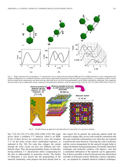
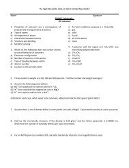
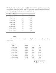
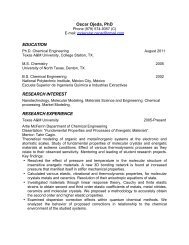
SEMINARIO et al.: NANOCELL: CHEMICALLY ASSEMBLED MOLECULAR ELECTRONIC CIRCUIT 1621Fig. 7. Single molecule and corresponding I–V characteristics for (a) single molecule featuring NDR and (b) two NDR molecules in series configuration; thissimplest configuration of a combined molecular circuit features multivalued characteristics that are used for programmability. (c) Combination of three of thesedevices already shows characteristics not observed in any other bulk device; the level of programmability can be further controlled by a third gate. This complexityincreases until we get to addressable circuits connected to microelectronic interfaces, as the one shown in Fig. 6 [3], [4], [12], [17], [28], [104]–[106], [110], [111].Fig. 8.Possible bottom-up approach to the fabrication of a nanocell IC on a top-down substrate.Fig. 7 [3], [4], [12], [17], [28], [104]–[106], [110]. <strong>The</strong> singledevice shows a nonlinear I–V behavior, which is an NDR.If two of these devices are connected in series, the resultantI–V for the series circuits shows multivalued responses, asindicated in Fig. 7(b). For some bias voltages, the currentthrough the series circuit can have two different and welldefinedvalues. Thus, the programmability feature of moleculeshaving nonlinear I–V characteristics allows compensating forthe lack of addressability in molecular circuits. <strong>The</strong> burdenof fabrication is now passed into the programming of thenanocell; fortunately, some progress has been already done inthis respect [8]. In general, the molecular pattern inside thenanocell is unique; thus, no two cells would be constructed withthe same molecular conformation even when they are requiredto perform the same functions. Choosing the correct moleculesand the correct arrangement for the nanocell strongly helps toreduce the burden of programming them. Eventually, depositiontechniques and molecular synthesis will improve, such thata nonrandom fabrication of the nanocell can be approached.Fig. 8 shows a possible, at least for the present time, hierarchicalassembly of molecular systems. Molecules, clusters, nanotubes,etc., are prepared by standard chemical synthesis techniques,
1622 <strong>IEEE</strong> SENSORS JOURNAL, VOL. 6, NO. 6, DECEMBER 2006and the semiconductor chips are prepared by the standardlithographic techniques. <strong>The</strong>n, chemical assembly techniquesare used to make the nanocells, which can be manipulated toreconfigure into useful molecular circuits; combined assemblyand lithographic techniques would need to be used.VII. STATE OF THE ART ON NANOCELLSWork using the flow shown in Fig. 8 is underway with acharge-current technique in order to demonstrate the concept.Thus, nanocells are converted into nanosensors operatingelectronically and at optical and terahertz frequencies [112].Since the electrical characteristic of the nanocell depends onthe conductance of the molecules inside the cell, adding moremolecules will certainly change the electrical characteristics.Future designs most likely will involve MEPs to detect andprocess information combined with molecular vibrational statesto transport information. Several nanocells have been alreadyconstructed by Franzon at NCSU using gold and palladiumdiscontinuous films on silicon oxide substrates. Experiments onthese cells have been performed by Tour [113] at Rice Universityand by our group [11]. Reproducible NDR-like behaviorwas found from filaments and clusters between discontinuousgold films; thus, one of the major problems encountered in theseexperiments is the careful manipulation of gold needed to avoidelectromigration. However, a stable and repeatable behaviorhas been found when electromigration takes place, that couldalso be implemented as a bond-formation–bond-breakingapproach to process information. <strong>The</strong> theoretical explanationof the mechanism leading to electromigration in nanocellswas also reported [11], [28]. Both groups, Tour’s and ours, arealso studying the possibility of constructing nanocells withoutmetallic contacts using heavily doped semiconductors or carbonnanotubes, and plans exist to use biomolecules such as DNAor proteins in building less random architectures for chargelessapproaches. Tour et al. [10] reported the first assembly of ananocell with disordered arrays of molecules and Au islands,which exhibited reproducible switching behavior and memoryeffects at room temperature. Major efforts were also performedby Allara and co-workers at Pennsylvania State University,where gold clusters were used instead of discontinuous goldfilms in addition to extensive work on molecular self-assembly[114]–[119]. An extraordinary set of molecules for molecularcircuits has been synthesized, assembled, and measured byTour and co-workers at Rice [6], [16], [107], [108], [116],[120]–[143]; their suitable selection of molecules has beenthe actual drive for the development of molecular electronics.Several of these devices present highly nonlinear characteristicsneeded for the formation of programmable devices. <strong>The</strong> groupof Tour et al. [7] also performed simulations and demonstratedthe ability to program nanocells using genetic algorithmbasedsimulations. With some simplifying assumptions, theseresults showed that it is possible to use nanocells as NANDand XOR gates as well as a 1-bit adder. Later, these authorsconsidered connecting nanocells using bistable latches forsignal restoration for logic and memory to determine theviability of programming the nanocells [8], [144]. On the otherhand, our group has been involved in the study of the intrinsiccharacteristics of single molecules to perform programmablefunctions using high-level quantum chemistry methods andalso demonstrating theoretically the possibility of transmissionof signals through molecules and the processing of informationusing MEPs [12], [17]–[20], [86], [90], [96], [97], [106], [110],[111]. <strong>The</strong> next step for these two approaches is to perform theproof of concept experiments. This proof of concept needs tobe performed at present time for strategic reasons since CMOSdevices will be fabricated at atomistic scales sometime after2010 according to the ITRS-2004 [145] predictions, using theEUV 157-nm immersion lithography, which will reduce thefeature sizes to 16 nm by 2016. By considering the typical lagtime between concepts and commercialization, perhaps the useof molecules for computation can change the whole picturewithin no more than five years from now, certainly if enoughsupport is provided.ACKNOWLEDGMENT<strong>The</strong> authors would like to thank L. Yan, L. Agapito,M. Mondragon, M. Diaz, and N. Rangel for the discussions andhelp with the manuscript, which is also connected to the researchperformed by former members of our team: L. Cordova,P. Derosa, A. Zacarias, and B. Bozard. <strong>The</strong> authors would alsolike to thank long time collaborators Tour and Franzon.REFERENCES[1] Intel, 65-Nanometer Process Technology Extends Benefits ofMoore’sLaw. [Online]. Available: www.intel.com/technology/silicon/si08042.htm[2] ——, Intel Pentium D Processor 900 Sequence and Intel PentiumProcessor Extreme Edition 955, p. 107, Jan. 2006. Intel Datasheet.[3] J. M. Seminario and L. E. Cordova, “Toward multiple-valued configurablerandom molecular logic units,” in Proc. <strong>IEEE</strong> Nanotechnol. Conf.,2001, vol. 1, pp. 146–150.[4] J. M. Seminario, A. G. Zacarias, and P. A. Derosa, “Analysis of a dinitrobasedmolecular device,” J. Chem. Phys., vol. 116, no. 4, pp. 1671–1683,Jan. 2002.[5] J. M. Seminario, L. E. Cordova, and P. A. Derosa, “An Ab Initio approachto the calculation of current-voltage characteristics of programmablemolecular devices,” Proc. <strong>IEEE</strong>, vol. 91, no. 11, pp. 1958–1975,Nov. 2003.[6] J. M. Tour, M. A. Reed, J. M. Seminario, D. A. Allara, and P. A. Weiss,“<strong>Molecular</strong> computer,” U.S. Patent 6 430 511, Aug. 6, 2002.[7] J. M. Tour, W. L. VanZandt, C. P. Husband, S. M. Husband, L. S. Wilson,P. D. Franzon, and D. P. Nackashi, “NanoCell logic gates for molecularcomputing,” <strong>IEEE</strong> Trans. Nanotechnol., vol. 1, no. 2, pp. 100–109,Jun. 2002.[8] C. P. Husband, S. M. Husband, J. S. Daniels, and J. M. Tour, “Logic andmemory with nanocell circuits,” <strong>IEEE</strong> Trans. Electron Devices, vol. 50,no. 9, pp. 1865–1875, Sep. 2003.[9] J. M. Tour, <strong>Molecular</strong> electronics. Commercial insights, chemistry,devices, architecture and programming. Singapore: World Scientific,2003.[10] J. M. Tour, L. Cheng, D. P. Nackashi, Y. Yao, A. K. Flatt,S. K. St. Angelo, T. E. Mallouk, and P. D. Franzon, “NanoCell electronicmemories,” J. Amer. Chem. Soc., vol. 125, no. 43, pp. 13279–13283,2003.[11] J .M. Seminario, Y. Ma, L. A. Agapito, L. Yan, R. A. Araujo, S. Bingi,N. S. Vadlamani, K. Chagarlamudi, T. S. Sudarshan, M. L. Myrick,P. E. Colavita, P. D. Franzon, D. P. Nackashi, L. Cheng, Y. Yao, andJ. M. Tour, “Clustering effects on discontinuous gold film nanocells,”J. Nanosci. Nanotechnol., vol. 4, no. 7, pp. 907–917, Sep. 2004.[12] J. M. Seminario, “<strong>Molecular</strong> electronics: Approaching Reality,” Nat.Mater., vol. 4, no. 2, pp. 111–113, Feb. 2005.[13] J. Chen, J. Su, W. Wang, and M. A. Reed, “Electronic memory effects inself-assembled monolayer systems,” Phys. E, vol. 16, no. 1, pp. 17–23,Jan. 2003.
- Page 1 and 2: 1614 IEEE SENSORS JOURNAL, VOL. 6,
- Page 3 and 4: 1616 IEEE SENSORS JOURNAL, VOL. 6,
- Page 5 and 6: 1618 IEEE SENSORS JOURNAL, VOL. 6,
- Page 7: 1620 IEEE SENSORS JOURNAL, VOL. 6,
- Page 11 and 12: 1624 IEEE SENSORS JOURNAL, VOL. 6,
- Page 13: 1626 IEEE SENSORS JOURNAL, VOL. 6,