Infrared readout electronics for space science sensors - Eric Fossum
Infrared readout electronics for space science sensors - Eric Fossum
Infrared readout electronics for space science sensors - Eric Fossum

Create successful ePaper yourself
Turn your PDF publications into a flip-book with our unique Google optimized e-Paper software.
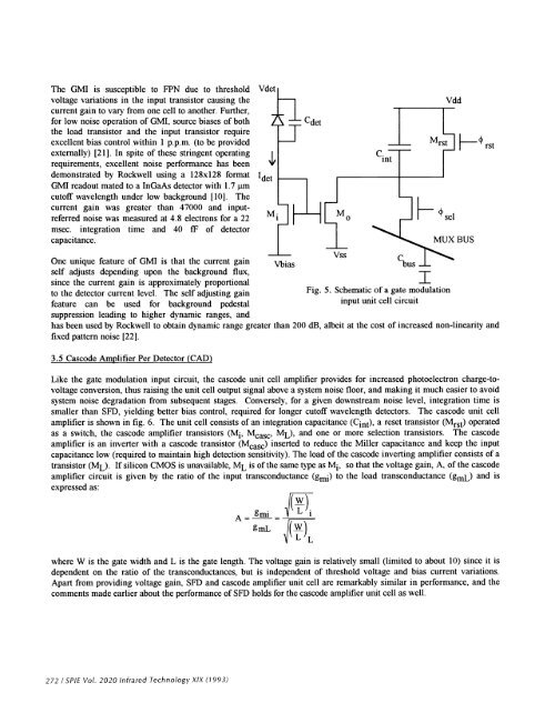
The GMI is susceptible to FPN due to thresholdvoltage variations in the input transistor causing theVddcurrent gain to vary from one cell to another. Further,<strong>for</strong> low noise operation of GMI, source biases of bothCdetthe load transistor and the input transistor requireexcellent bias control within 1 ppm. (to be providedi— i rstexternally) [2 1]. In spite of these stringent operatingrequirements, excellent noise per<strong>for</strong>mance has been "Idemonstrated by Rockwell using a 128x128 <strong>for</strong>mat 'detGMI <strong>readout</strong> mated to a InGaAs detector with 1.7 tmcutoff wavelength under low background [10]. Thecurrent gain was greater than 47000 and inputreferrednoise was measured at 4.8 electrons <strong>for</strong> a 22selmsec. integration time and 40 fF of detectorcapacitance.MUXBUSVssOne unique feature of GMI is that the current gainCv,iasbusself adjusts depending upon the background flux,since the current gain is approximately proportionalto the detector current level. The self adjusting gainFig. 5. Schematicofa gate modulationfeature can be used <strong>for</strong> background pedestalinput umt cell circuitsuppression leading to higher dynamic ranges, andhas been used by Rockwell to obtain dynamic range greater than 200 dB, albeit at the cost of increased non-linearity andfixed pattern noise [22].3.5 Cascode Amplifier Per Detector (CAD)Like the gate modulation input circuit, the cascode unit cell amplifier provides <strong>for</strong> increased photoelectron charge-tovoltageconversion, thus raising the unit cell output signal above a system noise floor, and making it much easier to avoidsystem noise degradation from subsequent stages. Conversely, <strong>for</strong> a given downstream noise level, integration time issmaller than SFD, yielding better bias control, required <strong>for</strong> longer cutoff wavelength detectors. The cascode unit cellamplifier is shown in fig. 6. The unit cell consists of an integration capacitance (Cint), a reset transistor (Mrst) operatedas a switch, the cascode amplifier transistors (M1, Mcasc, ML), and one or more selection transistors. The cascodeamplifier is an inverter with a cascode transistor (Mcasc) inserted to reduce the Miller capacitance and keep the inputcapacitance low (required to maintain high detection sensitivity). The load of the cascode inverting amplifier consists of atransistor (L) If silicon CMOS is unavailable, ML is of the same type as M, so that the voltage gain, A, of the cascodeamplifier circuit is given by the ratio of the input transconductance (gmi) to the load transconductance (g) and isexpressed as:A=--=1gmLi()\i LLwhere W is the gate width and L is the gate length. The voltage gain is relatively small (limited to about 10) since it isdependent on the ratio of the transconductances, but is independent of threshold voltage and bias current variations.Apart from providing voltage gain, SFD and cascode amplifier unit cell are remarkably similar in per<strong>for</strong>mance, and thecomments made earlier about the per<strong>for</strong>mance of SFD holds <strong>for</strong> the cascode amplifier unit cell as well.272 / SPIE Vol. 2020 <strong>Infrared</strong> Technology XIX (1993)