BRT 11, BRT 12, BRT 13 SITAC® AC Switches Without Zero Voltage ...
BRT 11, BRT 12, BRT 13 SITAC® AC Switches Without Zero Voltage ...
BRT 11, BRT 12, BRT 13 SITAC® AC Switches Without Zero Voltage ...

Create successful ePaper yourself
Turn your PDF publications into a flip-book with our unique Google optimized e-Paper software.
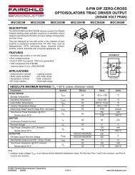
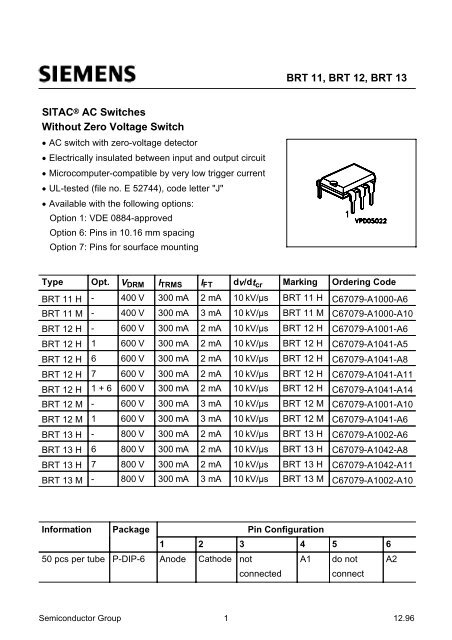
<strong>BRT</strong> <strong>11</strong>, <strong>BRT</strong> <strong>12</strong>, <strong>BRT</strong> <strong>13</strong>SIT<strong>AC</strong> ® <strong>AC</strong> <strong>Switches</strong><strong>Without</strong> <strong>Zero</strong> <strong>Voltage</strong> Switch• <strong>AC</strong> switch with zero-voltage detector• Electrically insulated between input and output circuit• Microcomputer-compatible by very low trigger current• UL-tested (file no. E 52744), code letter "J"• Available with the following options:Option 1: VDE 0884-approvedOption 6: Pins in 10.16 mm spacingOption 7: Pins for sourface mountingType Opt. V DRM I TRMS I FT dv/dt cr Marking Ordering Code<strong>BRT</strong> <strong>11</strong> H - 400 V 300 mA 2 mA 10 kV/µs <strong>BRT</strong> <strong>11</strong> H C67079-A1000-A6<strong>BRT</strong> <strong>11</strong> M - 400 V 300 mA 3 mA 10 kV/µs <strong>BRT</strong> <strong>11</strong> M C67079-A1000-A10<strong>BRT</strong> <strong>12</strong> H - 600 V 300 mA 2 mA 10 kV/µs <strong>BRT</strong> <strong>12</strong> H C67079-A1001-A6<strong>BRT</strong> <strong>12</strong> H 1 600 V 300 mA 2 mA 10 kV/µs <strong>BRT</strong> <strong>12</strong> H C67079-A1041-A5<strong>BRT</strong> <strong>12</strong> H 6 600 V 300 mA 2 mA 10 kV/µs <strong>BRT</strong> <strong>12</strong> H C67079-A1041-A8<strong>BRT</strong> <strong>12</strong> H 7 600 V 300 mA 2 mA 10 kV/µs <strong>BRT</strong> <strong>12</strong> H C67079-A1041-A<strong>11</strong><strong>BRT</strong> <strong>12</strong> H 1 + 6 600 V 300 mA 2 mA 10 kV/µs <strong>BRT</strong> <strong>12</strong> H C67079-A1041-A14<strong>BRT</strong> <strong>12</strong> M - 600 V 300 mA 3 mA 10 kV/µs <strong>BRT</strong> <strong>12</strong> M C67079-A1001-A10<strong>BRT</strong> <strong>12</strong> M 1 600 V 300 mA 3 mA 10 kV/µs <strong>BRT</strong> <strong>12</strong> M C67079-A1041-A6<strong>BRT</strong> <strong>13</strong> H - 800 V 300 mA 2 mA 10 kV/µs <strong>BRT</strong> <strong>13</strong> H C67079-A1002-A6<strong>BRT</strong> <strong>13</strong> H 6 800 V 300 mA 2 mA 10 kV/µs <strong>BRT</strong> <strong>13</strong> H C67079-A1042-A8<strong>BRT</strong> <strong>13</strong> H 7 800 V 300 mA 2 mA 10 kV/µs <strong>BRT</strong> <strong>13</strong> H C67079-A1042-A<strong>11</strong><strong>BRT</strong> <strong>13</strong> M - 800 V 300 mA 3 mA 10 kV/µs <strong>BRT</strong> <strong>13</strong> M C67079-A1002-A10Information Package Pin Configuration1 2 3 4 5 650 pcs per tube P-DIP-6 Anode Kathode Cathode notconnectedA1 do notconnectA2Semiconductor Group 1 <strong>12</strong>.96
<strong>BRT</strong> <strong>11</strong>, <strong>BRT</strong> <strong>12</strong>, <strong>BRT</strong> <strong>13</strong>Maximum Ratings, at Tj= 25 °C, unless otherwise specified.<strong>AC</strong> SwitchParameter Symbol Value UnitMax. Power dissipation P tot630 mWChip or operating temperature T j -40 ...+ 100 °CStorage temperature T stg -40 ...+ 150Insulation test voltage 1)between input/output circuit(climate in acc. with DIN 40046, part2, Nov.74)V IS5300 V RMSReference voltage in acc. with VDE 0<strong>11</strong>0 b(insulation group C)Creepage tracking resistance(in acc. with DIN IEC <strong>11</strong>2/VDE 0303, part 1)Insulation resistanceV IO = 500 V, T A = 25 °CV IO = 500 V, T A = 100 °CV refC TIR is500600175≥ 10 <strong>12</strong>≥ 10 <strong>11</strong>DIN humidity category, DIN 40 040 - F -Creepage distance (input/output circuit) - ≥ 7.2 mmClearance (input/output circuit) - ≥ 7.2Input CircuitParameter Symbol Value UnitParam VR V R 6 VContinuous forward current I F 20 mASurge forward current, I FSM(I) 1.5 AMax. power dissipation, , t ≤ 10 µsP tot 30 mWOutput CircuitParameter Symbol <strong>BRT</strong> <strong>BRT</strong><strong>11</strong> <strong>12</strong><strong>BRT</strong><strong>13</strong>V RMSV DC(group IIIaacc. to DINVDE 0109)ΩUnitRepetitive peak off-state voltage V DRM 400 600 800 VRMS on-state current I TRMS 300 mASingle cycle surge current (50 Hz) I TSM(I) 3 AMax. power dissipation P tot 600 mWSemiconductor Group 2 <strong>12</strong>.96
<strong>BRT</strong> <strong>11</strong>, <strong>BRT</strong> <strong>12</strong>, <strong>BRT</strong> <strong>13</strong>Characteristicsat Tj= 25 °C, unless otherwise specified.Input CircuitParameterForward <strong>Voltage</strong>,I F = 10 mAReverse current,V R = 6 VThermal resistance 2)junction - ambientSymbolValuesmin. typ. max.V F - 1.1 1.35 VI R- - 10UnitµAR thJA - - 750 K/WOutput CircuitParameter Symbol Values Unitmin. typ. max.Critical rate of rise of off-state voltagedv/dt crkV/µsV D = 0.67 V DRM , T j = 25 °CV D = 0.67 V DRM , T j = 80 °C105----Critical rate of rise of voltage at currentdv/dt crqcommunicationcommutationV D = 0.67 V DRM , T j = 25 °C, di/dt crq ≤ 15 A/ms10--V D = 0.67 V DRM , T j = 80 °C, di/dt crq ≤ 15 A/ms5--Critical rate of rise of on-state current di/dt cr 8 - - A/µsPulse currentt p ≤ 5 µs, f = 100 Hz, , di tp di /dt tp ≤ /dt 8 ≤ A/µs 8 A/µsOn-state voltage,I T = 300 mAOff-state currentT C = 100 °C, V DRM = V DRMI tp - - 2 AV T - - 2.3I D -V0.5 100 µAHolding current,V D = 10 VThermal resistance 2)junction - ambientI H - 80 500R thJA - - <strong>12</strong>5 K/WSemiconductor Group 3 <strong>12</strong>.96
Response Characteristicsat T j = 25 °C, unless otherwise specified.ParameterTrigger currentV D = 10 Vtype Htype MSymbolI FT<strong>BRT</strong> <strong>11</strong>, <strong>BRT</strong> <strong>12</strong>, <strong>BRT</strong> <strong>13</strong>Valuesmin. typ. max.0.40.8Trigger current temperature gradient ∆ I FT /∆ T j - 7Capacitance between input and output circuitV R = 0 V, f = 1 kHz--23UnitmA14 µA/KC IO - - 2 pF1) Test <strong>AC</strong> voltage in acc. with DIN 57883, June 19802) Static air, SIT<strong>AC</strong> soldered in pcb or base plate.3) The SIT<strong>AC</strong> switch is soldered in pcb or base plate.4) Thermocouple measurement has to be performed potentially separated to A1 and A2. The measuringjunction should be as near as possible at the case.Semiconductor Group 4 <strong>12</strong>.96
<strong>BRT</strong> <strong>11</strong>, <strong>BRT</strong> <strong>12</strong>, <strong>BRT</strong> <strong>13</strong>Characteristicsat Tj= 25 °C, unless otherwise specified.Typical input characteristicsIF = ƒ(VF)Typical output characteristicsIT = ƒ(VT)Current reduction ITRMS = ƒ(TA)R thJA = <strong>12</strong>5 K/W 3)Current reduction ITRMS = ƒ(TPIN5)RthJ-PIN5 = 16,5 K/W 4)Semiconductor Group 5 <strong>12</strong>.96
<strong>BRT</strong> <strong>11</strong>, <strong>BRT</strong> <strong>12</strong>, <strong>BRT</strong> <strong>13</strong>Typical trigger delay time tgd = f(IF/IFT25°C)VD = 200VPower dissipation for 40 ... 60 Hzline operationP tot = ƒ(ITRMS)Typical off-state current ID = f(Tj)VD = 800VPulse trigger current IFTN = f(tpIF)IFTN normalized to IFT refering to tpIF ≥ 1 msVop = 220 V, f= 40 ... 60 Hz typ.Semiconductor Group 6 <strong>12</strong>.96