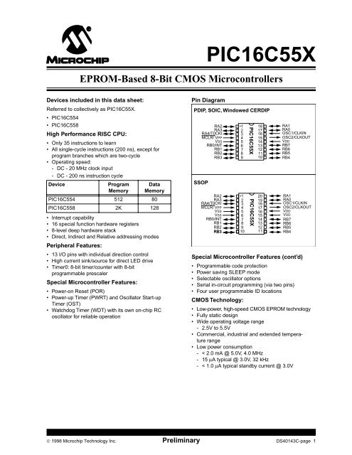
PIC16C55X, EPROM-Based 8-Bit CMOS MCU Data Sheet
PIC16C55X, EPROM-Based 8-Bit CMOS MCU Data Sheet
PIC16C55X, EPROM-Based 8-Bit CMOS MCU Data Sheet

You also want an ePaper? Increase the reach of your titles
YUMPU automatically turns print PDFs into web optimized ePapers that Google loves.
<strong>PIC16C55X</strong>NOTES:DS40143C-page 4 Preliminary © 1998 Microchip Technology Inc.
<strong>PIC16C55X</strong>1.0 GENERAL DESCRIPTIONThe <strong>PIC16C55X</strong> are 18 and 20-Pin <strong>EPROM</strong>-basedmembers of the versatile PIC16CXX family of low-cost,high-performance, <strong>CMOS</strong>, fully-static, 8-bitmicrocontrollers.All PICmicro ® microcontrollers employ an advancedRISC architecture. The <strong>PIC16C55X</strong> have enhancedcore features, eight-level deep stack, and multiple internaland external interrupt sources. The separateinstruction and data buses of the Harvard architectureallow a 14-bit wide instruction word with the separate8-bit wide data. The two-stage instruction pipelineallows all instructions to execute in a single-cycle,except for program branches (which require twocycles). A total of 35 instructions (reduced instructionset) are available. Additionally, a large register set givessome of the architectural innovations used to achieve avery high performance.<strong>PIC16C55X</strong> microcontrollers typically achieve a 2:1code compression and a 4:1 speed improvement overother 8-bit microcontrollers in their class.The PIC16C554 has 80 bytes of RAM. The PIC16C558has 128 bytes of RAM. Each device has 13 I/O pins andan 8-bit timer/counter with an 8-bit programmable prescaler.<strong>PIC16C55X</strong> devices have special features to reduceexternal components, thus reducing cost, enhancingsystem reliability and reducing power consumption.There are four oscillator options, of which the single pinRC oscillator provides a low-cost solution, the LPoscillator minimizes power consumption, XT is astandard crystal, and the HS is for High Speed crystals.The SLEEP (power-down) mode offers power saving.The user can wake up the chip from SLEEP throughseveral external and internal interrupts and reset.A highly reliable Watchdog Timer with its own on-chipRC oscillator provides protection against softwarelock-up.A UV-erasable CERDIP-packaged version is ideal forcode development while the cost-effective One-TimeProgrammable (OTP) version is suitable for productionin any volume.Table 1-1 shows the features of the <strong>PIC16C55X</strong>mid-range microcontroller families.A simplified block diagram of the <strong>PIC16C55X</strong> is shownin Figure 3-1.The <strong>PIC16C55X</strong> series fit perfectly in applicationsranging from motor control to low-power remote sensors.The <strong>EPROM</strong> technology makes customization ofapplication programs (detection levels, pulse generation,timers, etc.) extremely fast and convenient. Thesmall footprint packages make this microcontrollerseries perfect for all applications with space limitations.Low-cost, low-power, high-performance, ease of useand I/O flexibility make the <strong>PIC16C55X</strong> very versatile.1.1 Family and Upward CompatibilityThose users familiar with the PIC16C5X family ofmicrocontrollers will realize that this is an enhancedversion of the PIC16C5X architecture. Please refer toAppendix A for a detailed list of enhancements. Codewritten for PIC16C5X can be easily ported to<strong>PIC16C55X</strong> family of devices (Appendix B).The <strong>PIC16C55X</strong> family fills the niche for users wantingto migrate up from the PIC16C5X family and not needingvarious peripheral features of other members of thePIC16XX mid-range microcontroller family.1.2 Development SupportThe <strong>PIC16C55X</strong> family is supported by a full-featuredmacro assembler, a software simulator, an in-circuitemulator, a low-cost development programmer and afull-featured programmer. A “C” compiler and fuzzylogic support tools are also available.© 1998 Microchip Technology Inc. Preliminary DS40143C-page 5
<strong>PIC16C55X</strong>TABLE 1-1:<strong>PIC16C55X</strong> FAMILY OF DEVICESPIC16C554Clock Maximum Frequency of Operation (MHz) 20 20Memory<strong>EPROM</strong> Program Memory (x14 words) 512 2K<strong>Data</strong> Memory (bytes) 80 128Peripherals Timer Module(s) TMR0 TMR0FeaturesPIC16C558Interrupt Sources 3 3I/O Pins 13 13Voltage Range (Volts) 2.5-5.5 2.5-5.5Brown-out Reset — —Packages18-pin DIP,SOIC;20-pin SSOP18-pin DIP,SOIC;20-pin SSOPAll PICmicro ® Family devices have Power-on Reset, selectable Watchdog Timer, selectable code protect and highI/O current capability. All <strong>PIC16C55X</strong> Family devices use serial programming with clock pin RB6 and data pin RB7.DS40143C-page 6 Preliminary © 1998 Microchip Technology Inc.
<strong>PIC16C55X</strong>2.0 <strong>PIC16C55X</strong> DEVICE VARIETIESA variety of frequency ranges and packaging options areavailable. Depending on application and productionrequirements the proper device option can be selectedusing the information in the <strong>PIC16C55X</strong> ProductIdentification System section at the end of this datasheet. When placing orders, please use this page of thedata sheet to specify the correct part number.2.1 UV Erasable DevicesThe UV erasable version, offered in CERDIP packageis optimal for prototype development and pilotprograms. This version can be erased andreprogrammed to any of the oscillator modes.Microchip's PICSTART ® and PROMATE ®programmers both support programming of the<strong>PIC16C55X</strong>.2.2 One-Time-Programmable (OTP)DevicesThe availability of OTP devices is especially useful forcustomers who need the flexibility for frequent codeupdates and small volume applications. In addition tothe program memory, the configuration bits must alsobe programmed.2.3 Quick-Turnaround-Production (QTP)DevicesMicrochip offers a QTP Programming Service forfactory production orders. This service is madeavailable for users who choose not to program amedium to high quantity of units and whose code patternshave stabilized. The devices are identical to theOTP devices but with all <strong>EPROM</strong> locations and configurationoptions already programmed by the factory.Certain code and prototype verification proceduresapply before production shipments are available.Please contact your Microchip Technology sales officefor more details.2.4 SerializedQuick-Turnaround-Production(SQTP SM ) DevicesMicrochip offers a unique programming service wherea few user-defined locations in each device areprogrammed with different serial numbers. The serialnumbers may be random, pseudo-random orsequential.Serial programming allows each device to have aunique number which can serve as an entry-code,password or ID number.© 1998 Microchip Technology Inc. Preliminary DS40143C-page 7
<strong>PIC16C55X</strong>NOTES:DS40143C-page 8 Preliminary © 1998 Microchip Technology Inc.
<strong>PIC16C55X</strong>3.0 ARCHITECTURAL OVERVIEWThe high performance of the <strong>PIC16C55X</strong> family can beattributed to a number of architectural featurescommonly found in RISC microprocessors. To beginwith, the <strong>PIC16C55X</strong> uses a Harvard architecture, inwhich, program and data are accessed from separatememories using separate busses. This improvesbandwidth over traditional von Neumann architecturewhere program and data are fetched from the samememory. Separating program and data memory furtherallows instructions to be sized differently than 8-bitwide data words. Instruction opcodes are 14-bits widemaking it possible to have all single word instructions.A 14-bit wide program memory access bus fetches a14-bit instruction in a single cycle. A two-stage pipelineoverlaps fetch and execution of instructions.Consequently, all instructions (35) execute in a single-cycle(200 ns @ 20 MHz) except for programbranches. The table below lists the memory (E<strong>EPROM</strong>and ROM).DeviceProgramMemory<strong>Data</strong>MemoryPIC16C554 512 80PIC16C558 2K 128The PIC16C554 addresses 512 x 14 on-chip programmemory. The PIC16C558 addresses 2K x 14 programmemory. All program memory is internal.The <strong>PIC16C55X</strong> can directly or indirectly address itsregister files or data memory. All special functionregisters including the program counter are mappedinto the data memory. The <strong>PIC16C55X</strong> have anorthogonal (symmetrical) instruction set that makes itpossible to carry out any operation on any registerusing any addressing mode. This symmetrical natureand lack of ‘special optimal situations’ make programmingwith the <strong>PIC16C55X</strong> simple yet efficient. In addition,the learning curve is reduced significantly.The <strong>PIC16C55X</strong> devices contain an 8-bit ALU andworking register. The ALU is a general purposearithmetic unit. It performs arithmetic and Booleanfunctions between data in the working register and anyregister file.The ALU is 8-bits wide and capable of addition,subtraction, shift and logical operations. Unlessotherwise mentioned, arithmetic operations are two'scomplement in nature. In two-operand instructions,typically one operand is the working register(W register). The other operand is a file register or animmediate constant. In single operand instructions, theoperand is either the W register or a file register.The W register is an 8-bit working register used for ALUoperations. It is not an addressable register.Depending on the instruction executed, the ALU mayaffect the values of the Carry (C), Digit Carry (DC), andZero (Z) bits in the STATUS register. The C and DC bitsoperate as a Borrow and Digit Borrow out bit,respectively, in subtraction. See the SUBLW andSUBWF instructions for examples.A simplified block diagram is shown in Figure 3-1, witha description of the device pins in Table 3-1.© 1998 Microchip Technology Inc. Preliminary DS40143C-page 9
<strong>PIC16C55X</strong>FIGURE 3-1: BLOCK DIAGRAMDevicePIC16C554PIC16C558ProgramMemory512 x 142K x 14<strong>Data</strong> Memory(RAM)80 x 8128 x 8ProgramBus<strong>EPROM</strong>ProgramMemory512 x 14to2K x 1414Instruction reg13Program Counter8 Level Stack(13-bit)Direct Addr 7RAM Addr (1)<strong>Data</strong> BusRAMFileRegisters80 x 8 to128 x 88Addr MUX8FSR reg8IndirectAddrPORTAPORTBRA0RA1RA2RA3RA4/T0CKIRB0/INTRB7:RB18STATUS regPower-upTimer3MUXOSC1/CLKINOSC2/CLKOUTInstructionDecode &ControlTimingGenerationOscillatorStart-up TimerPower-onResetWatchdogTimer8ALUW regMCLRVDD, VSSTimer0Note 1: Higher order bits are from the status register.DS40143C-page 10 Preliminary © 1998 Microchip Technology Inc.
<strong>PIC16C55X</strong>FIGURE 4-3:DATA MEMORY MAP FORTHE PIC16C554FIGURE 4-4:DATA MEMORY MAP FORTHE PIC16C558FileAddressFileAddressFileAddressFileAddress00h01h02h03h04h05h06h07h08h09h0Ah0Bh0Ch0Dh0Eh0Fh10h11h12h13h14h15h16h17h18h19h1Ah1Bh1Ch1Dh1Eh1FhINDF (1)TMR0PCLSTATUSFSRPORTAPORTBPCLATHINTCONINDF (1)OPTIONPCLSTATUSFSRTRISATRISBPCLATHINTCONPCON80h81h82h83h84h85h86h87h88h89h8Ah8Bh8Ch8Dh8Eh8Fh90h91h92h93h94h95h96h97h98h99h9Ah9Bh9Ch9Dh9Eh9Fh00h01h02h03h04h05h06h07h08h09h0Ah0Bh0Ch0Dh0Eh0Fh10h11h12h13h14h15h16h17h18h19h1Ah1Bh1Ch1Dh1Eh1FhINDF (1)TMR0PCLSTATUSFSRPORTAPORTBPCLATHINTCONINDF (1)OPTIONPCLSTATUSFSRTRISATRISBPCLATHINTCONPCON80h81h82h83h84h85h86h87h88h89h8Ah8Bh8Ch8Dh8Eh8Fh90h91h92h93h94h95h96h97h98h99h9Ah9Bh9Ch9Dh9Eh9Fh20h6FhGeneralPurposeRegisterA0h20hGeneralPurposeRegisterGeneralPurposeRegisterA0hBFh70hC0h7FhBank 0 Bank 1FFh7FhBank 0 Bank 1FFhUnimplemented data memory locations, read as '0'.Note 1: Not a physical register.Unimplemented data memory locations, read as '0'.Note 1: Not a physical register.DS40143C-page 14 Preliminary © 1998 Microchip Technology Inc.
<strong>PIC16C55X</strong>4.2.2 SPECIAL FUNCTION REGISTERSThe Special Function Registers are registers used bythe CPU and peripheral functions for controlling thedesired operation of the device (Table 4-1). Theseregisters are static RAM.The special function registers can be classified into twosets (core and peripheral). The special function registersassociated with the “core” functions are describedin this section. Those related to the operation of theperipheral features are described in the section of thatperipheral feature.TABLE 4-1:SPECIAL REGISTERS FOR THE <strong>PIC16C55X</strong>Address Name <strong>Bit</strong> 7 <strong>Bit</strong> 6 <strong>Bit</strong> 5 <strong>Bit</strong> 4 <strong>Bit</strong> 3 <strong>Bit</strong> 2 <strong>Bit</strong> 1 <strong>Bit</strong> 0Value onPOR ResetValue onall otherresets (1)Bank 000h INDFAddressing this location uses contents of FSR to address data memory (not a physicalregister)xxxx xxxx xxxx xxxx01h TMR0 Timer0 Module’s Register xxxx xxxx uuuu uuuu02h PCL Program Counter's (PC) Least Significant Byte 0000 0000 0000 000003h STATUS IRP (2) RP1 (2) RP0 TO PD Z DC C 0001 1xxx 000q quuu04h FSR Indirect data memory address pointer xxxx xxxx uuuu uuuu05h PORTA — — — RA4 RA3 RA2 RA1 RA0 ---x xxxx ---u uuuu06h PORTB RB7 RB6 RB5 RB4 RB3 RB2 RB1 RB0 xxxx xxxx uuuu uuuu07h Unimplemented — —08h Unimplemented — —09h Unimplemented — —0Ah PCLATH — — — Write buffer for upper 5 bits of program counter ---0 0000 ---0 00000Bh INTCON GIE (3) T0IE INTE RBIE T0IF INTF RBIF 0000 000x 0000 000u0Ch Unimplemented — —0Dh-1Eh Unimplemented — —1Fh Unimplemented — —Bank 180h INDFAddressing this location uses contents of FSR to address data memory (not a physical xxxx xxxx xxxx xxxxregister)81h OPTION RBPU INTEDG T0CS T0SE PSA PS2 PS1 PS0 1111 1111 1111 111182h PCL Program Counter's (PC) Least Significant Byte 0000 0000 0000 000083h STATUS — — RP0 TO PD Z DC C 0001 1xxx 000q quuu84h FSR Indirect data memory address pointer xxxx xxxx uuuu uuuu85h TRISA — — — TRISA4 TRISA3 TRISA2 TRISA1 TRISA0 ---1 1111 ---1 111186h TRISB TRISB7 TRISB6 TRISB5 TRISB4 TRISB3 TRISB2 TRISB1 TRISB0 1111 1111 1111 111187h Unimplemented — —88h Unimplemented — —89h Unimplemented — —8Ah PCLATH — — — Write buffer for upper 5 bits of program counter ---0 0000 ---0 00008Bh INTCON GIE (3) T0IE INTE RBIE T0IF INTF RBIF 0000 000x 0000 000u8Ch Unimplemented — —8Dh Unimplemented — —8Eh PCON — — — — — — POR — ---- --0- ---- --u-8Fh-9Eh Unimplemented — —9Fh Unimplemented — —Legend: — = Unimplemented locations read as ‘0’, u = unchanged, x = unknown, q = value depends on condition,shaded = unimplementedNote 1: Other (non power-up) resets include MCLR reset and Watchdog Timer reset during normal operation.Note 2: IRP & RP1bits are reserved, always maintain these bits clear.Note 3: <strong>Bit</strong> 6 of INTCON register is reserved for future use. Always maintain this bit as clear.© 1998 Microchip Technology Inc. Preliminary DS40143C-page 15
<strong>PIC16C55X</strong>4.2.2.2 OPTION REGISTERThe OPTION register is a readable and writableregister which contains various control bits to configurethe TMR0/WDT prescaler, the external RB0/INTinterrupt, TMR0 and the weak pull-ups on PORTB.Note:To achieve a 1:1 prescaler assignment forTMR0, assign the prescaler to the WDT(PSA = 1).FIGURE 4-6: OPTION REGISTER (ADDRESS 81H)R/W-1 R/W-1 R/W-1 R/W-1 R/W-1 R/W-1 R/W-1 R/W-1RBPU INTEDG T0CS T0SE PSA PS2 PS1 PS0 R = Readable bitbit7bit0 W = Writable bit- n = Value at POR resetbit 7: RBPU: PORTB Pull-up Enable bit1 = PORTB pull-ups are disabled0 = PORTB pull-ups are enabled by individual port latch valuesbit 6: INTEDG: Interrupt Edge Select bit1 = Interrupt on rising edge of RB0/INT pin0 = Interrupt on falling edge of RB0/INT pinbit 5: T0CS: TMR0 Clock Source Select bit1 = Transition on RA4/T0CKI pin0 = Internal instruction cycle clock (CLKOUT)bit 4: T0SE: TMR0 Source Edge Select bit1 = Increment on high-to-low transition on RA4/T0CKI pin0 = Increment on low-to-high transition on RA4/T0CKI pinbit 3: PSA: Prescaler Assignment bit1 = Prescaler is assigned to the WDT0 = Prescaler is assigned to the Timer0 modulebit 2-0: PS2:PS0: Prescaler Rate Select bits<strong>Bit</strong> Value TMR0 Rate WDT Rate0000010100111001011101111 : 21 : 41 : 81 : 161 : 321 : 641 : 1281 : 2561 : 11 : 21 : 41 : 81 : 161 : 321 : 641 : 128© 1998 Microchip Technology Inc. Preliminary DS40143C-page 17
<strong>PIC16C55X</strong>4.2.2.3 INTCON REGISTERThe INTCON register is a readable and writableregister which contains the various enable and flag bitsfor all interrupt sources.Note:Interrupt flag bits get set when an interruptcondition occurs regardless of the state ofits corresponding enable bit or the globalenable bit, GIE (INTCON).FIGURE 4-7:INTCON REGISTER (ADDRESS 0BH OR 8BH)R/W-0 Reserved R/W-0 R/W-0 R/W-0 R/W-0 R/W-0 R/W-xGIE — T0IE INTE RBIE T0IF INTF RBIF R = Readable bitbit7bit0 W = Writable bit- n = Value at POR reset- x = Unknown at POR resetbit 7: GIE: Global Interrupt Enable bit1 = Enables all un-masked interrupts0 = Disables all interruptsbit 6: — = Reserved for future use. Always maintain this bit clear.bit 5: T0IE: TMR0 Overflow Interrupt Enable bit1 = Enables the TMR0 interrupt0 = Disables the TMR0 interruptbit 4: INTE: RB0/INT External Interrupt Enable bit1 = Enables the RB0/INT external interrupt0 = Disables the RB0/INT external interruptbit 3: RBIE: RB Port Change Interrupt Enable bit1 = Enables the RB port change interrupt0 = Disables the RB port change interruptbit 2: T0IF: TMR0 Overflow Interrupt Flag bit1 = TMR0 register has overflowed (must be cleared in software)0 = TMR0 register did not overflowbit 1: INTF: RB0/INT External Interrupt Flag bit1 = The RB0/INT external interrupt occurred (must be cleared in software)0 = The RB0/INT external interrupt did not occurbit 0: RBIF: RB Port Change Interrupt Flag bit1 = When at least one of the RB7:RB4 pins changed state (must be cleared in software)0 = None of the RB7:RB4 pins have changed stateDS40143C-page 18 Preliminary © 1998 Microchip Technology Inc.
<strong>PIC16C55X</strong>4.2.2.4 PCON REGISTERThe PCON register contains flag bits to differentiatebetween a Power-on Reset, an external MCLR reset orWDT reset. See Section 7.3 and Section 7.4 fordetailed reset operation.FIGURE 4-8:PCON REGISTER (ADDRESS 8Eh)U-0 U-0 U-0 U-0 U-0 U-0 R/W-0 U-0— — — — — — POR — R = Readable bitbit7bit0 W = Writable bitU = Unimplemented bit,read as ‘0’- n = Value at POR resetbit 7-2: Unimplemented: Read as '0'bit 1: POR: Power-on Reset Status bit1 = No Power-on Reset occurred0 = Power-on Reset occurredbit 0: Unimplemented: Read as '0'© 1998 Microchip Technology Inc. Preliminary DS40143C-page 19
<strong>PIC16C55X</strong>4.3 PCL and PCLATHThe program counter (PC) is 13-bits wide. The low bytecomes from the PCL register, which is a readable andwritable register. The high bits (PC) are not directlyreadable or writable and come from PCLATH. On anyreset, the PC is cleared. Figure 4-9 shows the twosituations for the loading of the PC. The upper example inthe figure shows how the PC is loaded on a write to PCL(PCLATH → PCH). The lower example in Figure 4-9shows how the PC is loaded during a CALL or GOTOinstruction (PCLATH → PCH).FIGURE 4-9:PCPCPCHLOADING OF PC INDIFFERENT SITUATIONS12 8 7 05PCHPCLATHPCLATHPCLPCL12 11 10 8 708Instruction withPCL asDestinationALU resultGOTO, CALL4.3.2 STACKThe <strong>PIC16C55X</strong> family has an 8 level deep x 13-bitwide hardware stack (Figure 4-1 and Figure 4-2). Thestack space is not part of either program or data spaceand the stack pointer is not readable or writable. ThePC is PUSHed onto the stack when a CALL instructionis executed or an interrupt causes a branch. The stackis POPed in the event of a RETURN, RETLW or a RETFIEinstruction execution. PCLATH is not affected by aPUSH or POP operation.The stack operates as a circular buffer. This means thatafter the stack has been PUSHed eight times, the ninthpush overwrites the value that was stored from the firstpush. The tenth push overwrites the second push (andso on).Note 1: There are no STATUS bits to indicatestack overflow or stack underflowconditions.Note 2: There are no instructions mnemonicscalled PUSH or POP. These are actionsthat occur from the execution of theCALL, RETURN, RETLW and RETFIEinstructions, or vectoring to an interruptaddress.2PCLATH11Opcode PCLATH4.3.1 COMPUTED GOTOA computed GOTO is accomplished by adding anoffset to the program counter (ADDWF PCL). Whendoing a table read using a computed GOTO method,care should be exercised if the table location crosses aPCL memory boundary (each 256 byte block). Refer tothe application note “Implementing a Table Read"(AN556).DS40143C-page 20 Preliminary © 1998 Microchip Technology Inc.
<strong>PIC16C55X</strong>4.4 Indirect Addressing, INDF and FSRRegistersThe INDF register is not a physical register. Addressingthe INDF register will cause indirect addressing.Indirect addressing is possible by using the INDF register.Any instruction using the INDF register actuallyaccesses data pointed to by the file select register(FSR). Reading INDF itself indirectly will produce 00h.Writing to the INDF register indirectly results in ano-operation (although status bits may be affected). Aneffective 9-bit address is obtained by concatenating the8-bit FSR register and the IRP bit (STATUS), asshown in Figure 4-10. However, IRP is not used in the<strong>PIC16C55X</strong>.A simple program to clear RAM locations 20h-2Fhusing indirect addressing is shown in Example 4-1.EXAMPLE 4-1:INDIRECT ADDRESSINGmovlw 0x20 ;initialize pointermovwf FSR ;to RAMNEXT clrf INDF ;clear INDF registerincf FSR ;inc pointerbtfss FSR,4 ;all done?goto NEXT ;no clear next;yes continueCONTINUE:FIGURE 4-10: DIRECT/INDIRECT ADDRESSING <strong>PIC16C55X</strong>Direct AddressingIndirect Addressing(1) RP1 RP0 6 from opcode 0IRP (1) 7 FSR register 0bank selectlocation selectbank selectlocation select00h00 01 10 1100h<strong>Data</strong>Memorynot used7FhBank 0 Bank 1 Bank 2 Bank 37FhFor memory map detail see Figure 4-3 and Figure 4-4.Note 1: The RP1 and IRP bits are reserved, always maintain these bits clear.© 1998 Microchip Technology Inc. Preliminary DS40143C-page 21
<strong>PIC16C55X</strong>NOTES:DS40143C-page 22 Preliminary © 1998 Microchip Technology Inc.
<strong>PIC16C55X</strong>5.0 I/O PORTSThe <strong>PIC16C55X</strong> have two ports, PORTA and PORTB.5.1 PORTA and TRISA RegistersPORTA is a 5-bit wide latch. RA4 is a Schmitt Trigger inputand an open drain output. Port RA4 is multiplexed with theT0CKI clock input. All other RA port pins have SchmittTrigger input levels and full <strong>CMOS</strong> output drivers. All pinshave data direction bits (TRIS registers) which can configurethese pins as input or output.A '1' in the TRISA register puts the corresponding outputdriver in a hi- impedance mode. A '0' in the TRISA registerputs the contents of the output latch on the selected pin(s).Reading the PORTA register reads the status of the pins,whereas writing to it will write to the port latch. All writeoperations are read-modify-write operations. So a writeto a port implies that the port pins are first read, then thisvalue is modified and written to the port data latch.Note:On reset, the TRISA register is set to all inputs.FIGURE 5-2:<strong>Data</strong>busWRPORTAWRTRISARD PORTADCKBLOCK DIAGRAM OF RA4 PIN<strong>Data</strong> LatchDCKQQQQTRISA LatchRD TRISAQSchmittTriggerinputbufferDENNVSSVSSI/O pin (1)FIGURE 5-1:BLOCK DIAGRAM OFPORT PINS RATMR0 clock input<strong>Data</strong>busDQWRPortACKQVDDPVDD<strong>Data</strong> LatchDQNI/O pinWRTRISACK QTRIS LatchVSSSchmittTriggerinputbufferVSSRD TRISAQDENRD PORTA© 1998 Microchip Technology Inc. Preliminary DS40143C-page 23
<strong>PIC16C55X</strong>TABLE 5-1:PORTA FUNCTIONSName <strong>Bit</strong> #BufferTypeFunctionRA0 bit0 ST Bi-directional I/O port.RA1 bit1 ST Bi-directional I/O port.RA2 bit2 ST Bi-directional I/O port.RA3 bit3 ST Bi-directional I/O port.RA4/T0CKI bit4 ST Bi-directional I/O port or external clock input for TMR0. Output is opendrain type.Legend: ST = Schmitt Trigger inputTABLE 5-2:SUMMARY OF REGISTERS ASSOCIATED WITH PORTAAddress Name <strong>Bit</strong> 7 <strong>Bit</strong> 6 <strong>Bit</strong> 5 <strong>Bit</strong> 4 <strong>Bit</strong> 3 <strong>Bit</strong> 2 <strong>Bit</strong> 1 <strong>Bit</strong> 0Value onPORValue onAll Other Resets05h PORTA — — — RA4 RA3 RA2 RA1 RA0 ---x xxxx ---u uuuu85h TRISA — — — TRISA4 TRISA3 TRISA2 TRISA1 TRISA0 ---1 1111 ---1 1111Legend: — = Unimplemented locations, read as ‘0’x = unknownu = unchangedNote: Shaded bits are not used by PORTA.DS40143C-page 24 Preliminary © 1998 Microchip Technology Inc.
<strong>PIC16C55X</strong>5.2 PORTB and TRISB RegistersPORTB is an 8-bit wide bi-directional port. Thecorresponding data direction register is TRISB. A '1' inthe TRISB register puts the corresponding output driverin a high impedance mode. A '0' in the TRISB registerputs the contents of the output latch on the selectedpin(s).Reading PORTB register reads the status of the pins,whereas writing to it will write to the port latch. All writeoperations are read-modify-write operations. So a writeto a port implies that the port pins are first read, thenthis value is modified and written to the port data latch.Each of the PORTB pins has a weak internal pull-up(≈200 µA typical). A single control bit can turn on all thepull-ups. This is done by clearing the RBPU(OPTION) bit. The weak pull-up is automaticallyturned off when the port pin is configured as an output.The pull-ups are disabled on Power-on Reset.Four of PORTB’s pins, RB7:RB4, have an interrupt onchange feature. Only pins configured as inputs cancause this interrupt to occur (i.e., any RB7:RB4 pinconfigured as an output is excluded from the interrupton change comparison). The input pins (of RB7:RB4)are compared with the old value latched on the lastread of PORTB. The “mismatch” outputs of RB7:RB4are OR’ed together to generate the RBIF interrupt (flaglatched in INTCON). This interrupt can wake thedevice from SLEEP. The user, in the interrupt serviceroutine, can clear the interrupt in the following manner:a) Any read or write of PORTB. This will end themismatch condition.b) Clear flag bit RBIF.A mismatch condition will continue to set flag bit RBIF.Reading PORTB will end the mismatch condition, andallow flag bit RBIF to be cleared.This interrupt on mismatch feature, together withsoftware configurable pull-ups on these four pins alloweasy interface to a key pad and make it possible forwake-up on key-depression. (See AN552 in theMicrochip Embedded Control Handbook.)Note:If a change on the I/O pin should occur when theread operation is being executed (start of the Q2cycle), then the RBIF interrupt flag may notget set.The interrupt on change feature is recommended forwake-up on key depression operation and operationswhere PORTB is only used for the interrupt on changefeature. Polling of PORTB is not recommended whileusing the interrupt on change feature.FIGURE 5-3:BLOCK DIAGRAM OF RB7:RB4 PINSRBPU (1)VDD<strong>Data</strong> busWR PortBWR TRISB<strong>Data</strong> LatchD QCKTRIS LatchD QCK QVDDPNVSSPTTLInputBufferweakpull-upSTBufferVDDVSSI/OpinSet RBIFRD TRISBRD PortBLatchQ DENFrom otherQRB7:RB4 pinsRB7:RB6 in serial programming modeENDRD Port BNote 1: TRISB = 1 enables weak pull-up if RBPU = '0'(OPTION).© 1998 Microchip Technology Inc. Preliminary DS40143C-page 25
<strong>PIC16C55X</strong>FIGURE 5-4:BLOCK DIAGRAM OF RB3:RB0 PINSRBPU (1)VDD<strong>Data</strong> busWR PortBWR TRISB<strong>Data</strong> LatchD QCKTRIS LatchD QCK QVDDPNVSSPTTLInputBufferweakpull-upSTBufferVDDVSSI/OpinRD TRISBRD PortBLatchQ DENRB0:INTSTBufferRD Port BNote 1: TRISB = 1 enables weak pull-up if RBPU = '0'(OPTION).TABLE 5-3:PORTB FUNCTIONSName <strong>Bit</strong> # Buffer Type FunctionRB0/INT bit0 TTL/ST (1) Input/output or external interrupt input. Internal software programmableweak pull-up.RB1 bit1 TTL Input/output pin. Internal software programmable weak pull-up.RB2 bit2 TTL Input/output pin. Internal software programmable weak pull-up.RB3 bit3 TTL Input/output pin. Internal software programmable weak pull-up.RB4 bit4 TTL Input/output pin (with interrupt on change). Internal softwareprogrammable weak pull-up.RB5 bit5 TTL Input/output pin (with interrupt on change). Internal softwareprogrammable weak pull-up.RB6 bit6 TTL/ST (2) Input/output pin (with interrupt on change). Internal softwareprogrammable weak pull-up. Serial programming clock pin.RB7 bit7 TTL/ST (2) Input/output pin (with interrupt on change). Internal softwareprogrammable weak pull-up. Serial programming data pin.Legend: ST = Schmitt Trigger, TTL = TTL inputNote 1: This buffer is a Schmitt Trigger input when configured as the external interrupt.Note 2: This buffer is a Schmitt Trigger input when used in serial programming mode.TABLE 5-4:SUMMARY OF REGISTERS ASSOCIATED WITH PORTBAddress Name <strong>Bit</strong> 7 <strong>Bit</strong> 6 <strong>Bit</strong> 5 <strong>Bit</strong> 4 <strong>Bit</strong> 3 <strong>Bit</strong> 2 <strong>Bit</strong> 1 <strong>Bit</strong> 0Value onPORValue onAll Other Rests06h PORTB RB7 RB6 RB5 RB4 RB3 RB2 RB1 RB0 xxxx xxxx uuuu uuuu86h TRISB TRISB7 TRISB6 TRISB5 TRISB4 TRISB3 TRISB2 TRISB1 TRISB0 1111 1111 1111 111181h OPTION RBPU INTEDG T0CS T0SE PSA PS2 PS1 PS0 1111 1111 1111 1111Legend:Note:x = unknown, u = unchangedShaded bits are not used by PORTB.DS40143C-page 26 Preliminary © 1998 Microchip Technology Inc.
<strong>PIC16C55X</strong>5.3 I/O Programming Considerations5.3.1 BI-DIRECTIONAL I/O PORTSAny instruction which writes, operates internally as aread followed by a write operation. The BCF and BSFinstructions, for example, read the register into theCPU, execute the bit operation and write the result backto the register. Caution must be used when theseinstructions are applied to a port with both inputs andoutputs defined. For example, a BSF operation on bit5of PORTB will cause all eight bits of PORTB to be readinto the CPU. Then the BSF operation takes place onbit5 and PORTB is written to the output latches. Ifanother bit of PORTB is used as a bidirectional I/O pin(e.g., bit0) and it is defined as an input at this time, theinput signal present on the pin itself would be read intothe CPU and re-written to the data latch of thisparticular pin, overwriting the previous content. As longas the pin stays in the input mode, no problem occurs.However, if bit0 is switched into output mode later on,the content of the data latch may now be unknown.Reading the port register, reads the values of the portpins. Writing to the port register writes the value to theport latch. When using read modify write instructions(ex. BCF, BSF, etc.) on a port, the value of the port pinsis read, the desired operation is done to this value, andthis value is then written to the port latch.Example 5-1 shows the effect of two sequentialread-modify-write instructions (ex., BCF, BSF, etc.) onan I/O port.A pin actively outputting a Low or High should not bedriven from external devices at the same time in orderto change the level on this pin (“wired-or”, “wired-and”).The resulting high output currents may damagethe chip.EXAMPLE 5-1: READ-MODIFY-WRITEINSTRUCTIONS ON ANI/O PORT; Initial PORT settings: PORTB Inputs;; PORTB Outputs; PORTB have external pull-up and are not; connected to other circuitry;; PORT latch PORT pins; ---------- ----------BCF PORTB, 7 ; 01pp pppp 11pp ppppBCF PORTB, 6 ; 10pp pppp 11pp ppppBSF STATUS,RP0 ;BCF TRISB, 7 ; 10pp pppp 11pp ppppBCF TRISB, 6 ; 10pp pppp 10pp pppp;; Note that the user may have expected the pin; values to be 00pp pppp. The 2nd BCF caused; RB7 to be latched as the pin value (High).5.3.2 SUCCESSIVE OPERATIONS ON I/O PORTSThe actual write to an I/O port happens at the end of aninstruction cycle, whereas for reading, the data must bevalid at the beginning of the instruction cycle(Figure 5-5). Therefore, care must be exercised if awrite followed by a read operation is carried out on thesame I/O port. The sequence of instructions should besuch to allow the pin voltage to stabilize (loaddependent) before the next instruction which causesthat file to be read into the CPU is executed. Otherwise,the previous state of that pin may be read into the CPUrather than the new state. When in doubt, it is better toseparate these instructions with an NOP or anotherinstruction not accessing this I/O port.FIGURE 5-5:SUCCESSIVE I/O OPERATIONPCInstructionfetchedRB7:RB0Q1 Q2 Q3 Q4 Q1 Q2 Q3 Q4 Q1 Q2 Q3 Q4 Q1 Q2 Q3 Q4PC PC + 1 PC + 2 PC + 3MOVWF PORTBWrite toPORTBMOVF PORTB, WRead PORTBNOPNOPTPDExecuteMOVWFPORTBPort pinsampled hereExecuteMOVFPORTB, WExecuteNOPNote:This example shows write to PORTBfollowed by a read from PORTB.Note that:data setup time = (0.25 TCY - TPD)where TCY = instruction cycle andTPD = propagation delay of Q1 cycleto output valid.Therefore, at higher clock frequencies,a write followed by a read may beproblematic.© 1998 Microchip Technology Inc. Preliminary DS40143C-page 27
<strong>PIC16C55X</strong>NOTES:DS40143C-page 28 Preliminary © 1998 Microchip Technology Inc.
<strong>PIC16C55X</strong>6.0 TIMER0 MODULEThe Timer0 module timer/counter has the followingfeatures:• 8-bit timer/counter• Readable and writable• 8-bit software programmable prescaler• Internal or external clock select• Interrupt on overflow from FFh to 00h• Edge select for external clockFigure 6-1 is a simplified block diagram of the Timer0module.Timer mode is selected by clearing the T0CS bit(OPTION). In timer mode, the TMR0 will incrementevery instruction cycle (without prescaler). If Timer0 iswritten, the increment is inhibited for the following twocycles (Figure 6-2 and Figure 6-3). The user can workaround this by writing an adjusted value to TMR0.Counter mode is selected by setting the T0CS bit. Inthis mode Timer0 will increment either on every risingor falling edge of pin RA4/T0CKI. The incrementingedge is determined by the source edge (T0SE) controlbit (OPTION). Clearing the T0SE bit selects therising edge. Restrictions on the external clock input arediscussed in detail in Section 6.2.The prescaler is shared between the Timer0 moduleand the WatchdogTimer. The prescaler assignment iscontrolled in software by the control bit PSA(OPTION). Clearing the PSA bit will assign theprescaler to Timer0. The prescaler is not readable orwritable. When the prescaler is assigned to the Timer0module, prescale value of 1:2, 1:4, ..., 1:256 areselectable. Section 6.3 details the operation of theprescaler.6.1 TIMER0 InterruptTimer0 interrupt is generated when the TMR0 registertimer/counter overflows from FFh to 00h. This overflowsets the T0IF bit. The interrupt can be masked byclearing the T0IE bit (INTCON). The T0IF bit(INTCON) must be cleared in software by theTimer0 module interrupt service routine beforere-enabling this interrupt. The Timer0 interrupt cannotwake the processor from SLEEP since the timer is shutoff during SLEEP. See Figure 6-4 for Timer0 interrupttiming.FIGURE 6-1:TIMER0 BLOCK DIAGRAMRA4/T0CKI FOSC/4pinT0SE01ProgrammablePrescaler10PSoutSync withInternalclocks(2 Tcy delay)PSout<strong>Data</strong> busTMR08T0CSPS2:PS0PSASet Flag bit T0IFon OverflowNote 1: <strong>Bit</strong>s, T0SE, T0CS, PS2, PS1, PS0 and PSA are located in the OPTION register.2: The prescaler is shared with Watchdog Timer (Figure 6-6)FIGURE 6-2:TIMER0 (TMR0) TIMING: INTERNAL CLOCK/NO PRESCALERPC(ProgramCounter)InstructionFetchQ1 Q2 Q3 Q4 Q1 Q2 Q3 Q4 Q1 Q2 Q3 Q4 Q1 Q2 Q3 Q4 Q1 Q2 Q3 Q4 Q1 Q2 Q3 Q4 Q1 Q2 Q3 Q4 Q1 Q2 Q3 Q4PC-1PC PC+1 PC+2 PC+3 PC+4 PC+5 PC+6MOVWF TMR0 MOVF TMR0,W MOVF TMR0,W MOVF TMR0,W MOVF TMR0,W MOVF TMR0,WTMR0T0 T0+1 T0+2 NT0 NT0 NT0 NT0+1 NT0+2 T0InstructionExecutedWrite TMR0executedRead TMR0reads NT0Read TMR0reads NT0Read TMR0reads NT0Read TMR0reads NT0 + 1Read TMR0reads NT0 + 2© 1998 Microchip Technology Inc. Preliminary DS40143C-page 29
<strong>PIC16C55X</strong>FIGURE 6-3: TIMER0 TIMING: INTERNAL CLOCK/PRESCALE 1:2PC(ProgramCounter)InstructionFetchQ1 Q2 Q3 Q4 Q1 Q2 Q3 Q4 Q1 Q2 Q3 Q4 Q1 Q2 Q3 Q4 Q1 Q2 Q3 Q4 Q1 Q2 Q3 Q4 Q1 Q2 Q3 Q4 Q1 Q2 Q3 Q4PC-1PC PC+1 PC+2 PC+3 PC+4 PC+5 PC+6MOVWF TMR0 MOVF TMR0,W MOVF TMR0,W MOVF TMR0,W MOVF TMR0,W MOVF TMR0,WTMR0T0T0+1 NT0NT0+1InstructionExecuteWrite TMR0executedRead TMR0reads NT0Read TMR0reads NT0Read TMR0reads NT0Read TMR0reads NT0Read TMR0reads NT0 + 1FIGURE 6-4:TIMER0 INTERRUPT TIMINGQ1 Q2 Q3 Q4 Q1 Q2 Q3 Q4 Q1 Q2 Q3 Q4 Q1 Q2 Q3 Q4 Q1 Q2 Q3 Q4OSC1CLKOUT(3)TMR0 timerT0IF bit(INTCON)FEh1 1FFh 00h 01h 02hGIE bit(INTCON)INSTRUCTION FLOWPCInterrupt Latency TimePC PC +1 PC +1 0004h 0005hInstructionfetchedInst (PC)Inst (PC+1)Inst (0004h)Inst (0005h)InstructionexecutedInst (PC-1)Inst (PC)Dummy cycleDummy cycleInst (0004h)Note 1: T0IF interrupt flag is sampled here (every Q1).2: Interrupt latency = 4Tcy, where Tcy = instruction cycle time.3: CLKOUT is available only in RC oscillator mode.DS40143C-page 30 Preliminary © 1998 Microchip Technology Inc.
<strong>PIC16C55X</strong>6.2 Using Timer0 with External ClockWhen an external clock input is used for Timer0, it mustmeet certain requirements. The external clockrequirement is due to internal phase clock (TOSC)synchronization. Also, there is a delay in the actualincrementing of Timer0 after synchronization.6.2.1 EXTERNAL CLOCK SYNCHRONIZATIONWhen no prescaler is used, the external clock input isthe same as the prescaler output. The synchronizationof T0CKI with the internal phase clocks isaccomplished by sampling the prescaler output on theQ2 and Q4 cycles of the internal phase clocks(Figure 6-5). Therefore, it is necessary for T0CKI to behigh for at least 2TOSC (and a small RC delay of 20 ns)and low for at least 2TOSC (and a small RC delay of20 ns). Refer to the electrical specification of thedesired device.When a prescaler is used, the external clock input isdivided by the asynchronous ripple-counter typeprescaler so that the prescaler output is symmetrical.For the external clock to meet the samplingrequirement, the ripple-counter must be taken intoaccount. Therefore, it is necessary for T0CKI to have aperiod of at least 4TOSC (and a small RC delay of40 ns) divided by the prescaler value. The onlyrequirement on T0CKI high and low time is that they donot violate the minimum pulse width requirement of10 ns. Refer to parameters 40, 41 and 42 in theelectrical specification of the desired device.6.2.2 TIMER0 INCREMENT DELAYSince the prescaler output is synchronized with theinternal clocks, there is a small delay from the time theexternal clock edge occurs to the time the TMR0 isactually incremented. Figure 6-5 shows the delay fromthe external clock edge to the timer incrementing.FIGURE 6-5:TIMER0 TIMING WITH EXTERNAL CLOCKExternal Clock Input orPrescaler output (2)External Clock/PrescalerOutput after samplingIncrement Timer0 (Q4)Q1 Q2 Q3 Q4 Q1 Q2 Q3 Q4 Q1 Q2 Q3 Q4 Q1 Q2 Q3 Q4Small pulsemisses sampling(3)(1)Timer0 T0 T0 + 1 T0 + 2Note 1: Delay from clock input change to Timer0 increment is 3Tosc to 7Tosc. (Duration of Q = Tosc).Therefore, the error in measuring the interval between two edges on Timer0 input = ±4Tosc max.2: External clock if no prescaler selected, Prescaler output otherwise.3: The arrows indicate the points in time where sampling occurs.© 1998 Microchip Technology Inc. Preliminary DS40143C-page 31
<strong>PIC16C55X</strong>6.3 PrescalerAn 8-bit counter is available as a prescaler for theTimer0 module, or as a postscaler for the WatchdogTimer, respectively (Figure 6-6). For simplicity, thiscounter is being referred to as “prescaler” throughoutthis data sheet. Note that there is only one prescaleravailable which is mutually exclusive between theTimer0 module and the Watchdog Timer. Thus, aprescaler assignment for the Timer0 module meansthat there is no prescaler for the Watchdog Timer, andvice-versa.The PSA and PS2:PS0 bits (OPTION) determinethe prescaler assignment and prescale ratio.When assigned to the Timer0 module, all instructionswriting to the TMR0 register (e.g., CLRF 1, MOVWF 1,BSF 1,x....etc.) will clear the prescaler. Whenassigned to WDT, a CLRWDT instruction will clear theprescaler along with the Watchdog Timer. Theprescaler is not readable or writable.FIGURE 6-6:BLOCK DIAGRAM OF THE TIMER0/WDT PRESCALERCLKOUT (=Fosc/4)<strong>Data</strong> BusT0CKIpin0MU1X1 0MUXSYNC2Tcy8TMR0 regT0SET0CSPSASet flag bit T0IFon OverflowWatchdogTimer01MUX8-bit Prescaler8PSA8-to-1MUXPS0 - PS2WDT Enable bit0 1M U XPSAWDTTime-outNote: T0SE, T0CS, PSA, PS0-PS2 are bits in the OPTION register.DS40143C-page 32 Preliminary © 1998 Microchip Technology Inc.
<strong>PIC16C55X</strong>6.3.1 SWITCHING PRESCALER ASSIGNMENTThe prescaler assignment is fully under softwarecontrol (i.e., it can be changed “on the fly” duringprogram execution). To avoid an unintended deviceRESET, the following instruction sequence(Example 6-1) must be executed when changing theprescaler assignment from Timer0 to WDT. Lines 5-7are required only if the desired postscaler rate is 1:1(PS = 000) or 1:2 (PS = 001).EXAMPLE 6-1:CHANGING PRESCALER(TIMER0→WDT)1.BCF STATUS, RP0 ;Skip if already in; Bank 02.CLRWDT;Clear WDT3.CLRF TMR0 ;Clear TMR0 & Prescaler4.BSF STATUS, RP0 ;Bank 15.MOVLW '00101111’b; ;These 3 lines (5, 6, 7)6.MOVWF OPTION ; are required only if; desired PS are7.CLRWDT ; 000 or 0018.MOVLW '00101xxx’b ;Set Postscaler to9.MOVWF OPTION ; desired WDT rate10.BCF STATUS, RP0 ;Return to Bank 0To change prescaler from the WDT to the TMR0module use the sequence shown in Example 6-2. Thisprecaution must be taken even if the WDT is disabled.EXAMPLE 6-2:CHANGING PRESCALER(WDT→TIMER0)CLRWDT;Clear WDT and;prescalerBSF STATUS, RP0MOVLW b'xxxx0xxx' ;Select TMR0, new;prescale value and;clock sourceMOVWF OPTIONBCF STATUS, RP0TABLE 6-1:REGISTERS ASSOCIATED WITH TIMER0Address Name <strong>Bit</strong> 7 <strong>Bit</strong> 6 <strong>Bit</strong> 5 <strong>Bit</strong> 4 <strong>Bit</strong> 3 <strong>Bit</strong> 2 <strong>Bit</strong> 1 <strong>Bit</strong> 0Value onPORValue onAll Other Resets01h TMR0 Timer0 module’s register xxxx xxxx uuuu uuuu0Bh/8Bh INTCON GIE + T0IE INTE RBIE T0IF INTF RBIF 0000 000x 0000 000x81h OPTION RBPU INTEDG T0CS T0SE PSA PS2 PS1 PS0 1111 1111 1111 111185h TRISA — — — TRISA4 TRISA3 TRISA2 TRISA1 TRISA0 ---1 1111 ---1 1111Legend: — = Unimplemented locations, read as ‘0’.+ = Reserved for future use.Note: Shaded bits are not used by TMR0 module.© 1998 Microchip Technology Inc. Preliminary DS40143C-page 33
<strong>PIC16C55X</strong>NOTES:DS40143C-page 34 Preliminary © 1998 Microchip Technology Inc.
<strong>PIC16C55X</strong>7.0 SPECIAL FEATURES OF THECPUWhat sets a microcontroller apart from otherprocessors are special circuits to deal with the needs ofreal time applications. The <strong>PIC16C55X</strong> family has ahost of such features intended to maximize systemreliability, minimize cost through elimination of externalcomponents, provide power saving operating modesand offer code protection.These are:1. OSC selection2. ResetPower-on Reset (POR)Power-up Timer (PWRT)Oscillator Start-Up Timer (OST)3. Interrupts4. Watchdog Timer (WDT)5. SLEEP6. Code protection7. ID Locations8. In-circuit serial programmingThe <strong>PIC16C55X</strong> has a Watchdog Timer which iscontrolled by configuration bits. It runs off its own RCoscillator for added reliability. There are two timers thatoffer necessary delays on power-up. One is theOscillator Start-up Timer (OST), intended to keep thechip in reset until the crystal oscillator is stable. Theother is the Power-up Timer (PWRT), which provides afixed delay of 72 ms (nominal) on power-up only,designed to keep the part in reset while the powersupply stabilizes. With these two functions on-chip,most applications need no external reset circuitry.The SLEEP mode is designed to offer a very lowcurrent power-down mode. The user can wake-up fromSLEEP through external reset, Watchdog Timerwake-up or through an interrupt. Several oscillatoroptions are also made available to allow the part to fitthe application. The RC oscillator option saves systemcost while the LP crystal option saves power. A set ofconfiguration bits are used to select various options.© 1998 Microchip Technology Inc. Preliminary DS40143C-page 35
<strong>PIC16C55X</strong>7.1 Configuration <strong>Bit</strong>sThe configuration bits can be programmed (read as '0')or left unprogrammed (read as '1') to select variousdevice configurations. These bits are mapped inprogram memory location 2007h.The user will note that address 2007h is beyondthe user program memory space. In fact, it belongsto the special test/configuration memory space(2000h – 3FFFh), which can be accessed only duringprogramming.FIGURE 7-1:CONFIGURATION WORDCP1 CP0 1 CP1 CP0 1 CP1 CP0 1 — Reserved CP1 CP0 1 PWRTE WDTE F0SC1 F0SC0 CONFIG Addressbit13bit0 REGISTER: 2007hbit 13-8 CP: Code protection bits (1)5-4: 11 = Program Memory code protection off10 = 0400h - 07FFh code protected01 = 0200h - 07FFh code protected11 = 0000h - 07FFh code protectedbit 7: Unimplemented: Read as '1'bit 6: Reserved: Do not usebit 3:bit 2:bit 1-0:PWRTE: Power-up Timer Enable bit1 = PWRT disabled0 = PWRT enabledWDTE: Watchdog Timer Enable bit1 = WDT enabled0 = WDT disabledFOSC1:FOSC0: Oscillator Selection bits11 = RC oscillator10 = HS oscillator01 = XT oscillator00 = LP oscillatorNote 1: All of the CP1:CP0 pairs have to be given the same value to enable the code protection scheme listed.DS40143C-page 36 Preliminary © 1998 Microchip Technology Inc.
<strong>PIC16C55X</strong>7.2 Oscillator Configurations7.2.1 OSCILLATOR TYPESThe <strong>PIC16C55X</strong> can be operated in four differentoscillator options. The user can program twoconfiguration bits (FOSC1 and FOSC0) to select one ofthese four modes:• LP Low Power Crystal• XT Crystal/Resonator• HS High Speed Crystal/Resonator• RC Resistor/Capacitor7.2.2 CRYSTAL OSCILLATOR / CERAMICRESONATORSIn XT, LP or HS modes a crystal or ceramic resonatoris connected to the OSC1 and OSC2 pins to establishoscillation (Figure 7-2). The <strong>PIC16C55X</strong> oscillatordesign requires the use of a parallel cut crystal. Use ofa series cut crystal may give a frequency out of thecrystal manufacturers specifications. When in XT, LP orHS modes, the device can have an external clocksource to drive the OSC1 pin (Figure 7-3).TABLE 7-1:Ranges Characterized:CAPACITOR SELECTIONFOR CERAMIC RESONATORS(PRELIMINARY)Mode Freq OSC1(C1) OSC2(C2)XTHSTABLE 7-2:455 kHz2.0 MHz4.0 MHz8.0 MHz16.0 MHz22 - 100 pF15 - 68 pF15 - 68 pF10 - 68 pF10 - 22 pF22 - 100 pF15 - 68 pF15 - 68 pF10 - 68 pF10 - 22 pFHigher capacitance increases the stability of the oscillatorbut also increases the start-up time. These values are fordesign guidance only. Since each resonator has its owncharacteristics, the user should consult with the resonatormanufacturer for appropriate values of external components.CAPACITOR SELECTIONFOR CRYSTAL OSCILLATOR(PRELIMINARY)Mode Freq OSC1(C1) OSC2(C2)FIGURE 7-2:CRYSTAL OPERATION(OR CERAMIC RESONATOR)(HS, XT OR LP OSCCONFIGURATION)LPXT32 kHz200 kHz100 kHz2 MHz4 MHz68 - 100 pF15 - 30 pF68 - 150 pF15 - 30 pF15 - 30 pF68 - 100 pF15 - 30 pF150 - 200 pF15 - 30 pF15 - 30 pFC1C2See Table 7-1 and Table 7-2 for recommendedvalues of C1 and C2.Note:XTALRSsee NoteOSC1OSC2RFTo internal logicSLEEP<strong>PIC16C55X</strong>A series resistor may be required forAT strip cut crystals.HS8 MHz10 MHz20 MHz15 - 30 pF15 - 30 pF15 - 30 pF15 - 30 pF15 - 30 pF15 - 30 pFHigher capacitance increases the stability of the oscillatorbut also increases the start-up time. These values are fordesign guidance only. Rs may be required in HS mode aswell as XT mode to avoid overdriving crystals with low drivelevel specification. Since each crystal has its owncharacteristics, the user should consult with the crystalmanufacturer for appropriate values of external components.FIGURE 7-3:EXTERNAL CLOCK INPUTOPERATION (HS, XT OR LPOSC CONFIGURATION)Clock fromext. systemOpenOSC1<strong>PIC16C55X</strong>OSC2© 1998 Microchip Technology Inc. Preliminary DS40143C-page 37
<strong>PIC16C55X</strong>7.2.3 EXTERNAL CRYSTAL OSCILLATORCIRCUITEither a pre-packaged oscillator can be used or a simpleoscillator circuit with TTL gates can be built.Prepackaged oscillators provide a wide operatingrange and better stability. A well-designed crystaloscillator will provide good performance with TTLgates. Two types of crystal oscillator circuits can beused; one with series resonance, or one with parallelresonance.Figure 7-4 shows implementation of a parallel resonantoscillator circuit. The circuit is designed to use thefundamental frequency of the crystal. The 74AS04inverter performs the 180° phase shift that a paralleloscillator requires. The 4.7 kΩ resistor provides thenegative feedback for stability. The 10 kΩpotentiometers bias the 74AS04 in the linear region.This could be used for external oscillator designs.FIGURE 7-4:+5V10k4.7kEXTERNAL PARALLELRESONANT CRYSTALOSCILLATOR CIRCUIT74AS04XTAL10k74AS04To otherDevices<strong>PIC16C55X</strong>CLKIN7.2.4 RC OSCILLATORFor timing insensitive applications the “RC” deviceoption offers additional cost savings. The RC oscillatorfrequency is a function of the supply voltage, theresistor (Rext) and capacitor (Cext) values, and theoperating temperature. In addition to this, the oscillatorfrequency will vary from unit to unit due to normalprocess parameter variation. Furthermore, thedifference in lead frame capacitance between packagetypes will also affect the oscillation frequency,especially for low Cext values. The user also needs totake into account variation due to tolerance of externalR and C components used. Figure 7-6 shows how theR/C combination is connected to the <strong>PIC16C55X</strong>. ForRext values below 2.2 kΩ, the oscillator operation maybecome unstable, or stop completely. For very highRext values (e.g., 1 MΩ), the oscillator becomessensitive to noise, humidity and leakage. Thus, werecommend to keep Rext between 3 kΩ and 100 kΩ.Although the oscillator will operate with no externalcapacitor (Cext = 0 pF), we recommend using valuesabove 20 pF for noise and stability reasons. With no orsmall external capacitance, the oscillation frequencycan vary dramatically due to changes in externalcapacitances, such as PCB trace capacitance orpackage lead frame capacitance.The oscillator frequency, divided by 4, is available onthe OSC2/CLKOUT pin, and can be used for testpurposes or to synchronize other logic (Figure 3-2 forwaveform).FIGURE 7-6:RC OSCILLATOR MODE10k20 pF20 pFFigure 7-5 shows a series resonant oscillator circuit.This circuit is also designed to use the fundamentalfrequency of the crystal. The inverter performs a 180°phase shift in a series resonant oscillator circuit. The330 Ω resistors provide the negative feedback to biasthe inverters in their linear region.VDDRextCextVDDFosc/4<strong>PIC16C55X</strong>OSC1Internal ClockOSC2/CLKOUTFIGURE 7-5:EXTERNAL SERIESRESONANT CRYSTALOSCILLATOR CIRCUIT330 Ω74AS04330 Ω74AS04To otherDevices<strong>PIC16C55X</strong>74AS040.1 µFCLKINXTALDS40143C-page 38 Preliminary © 1998 Microchip Technology Inc.
<strong>PIC16C55X</strong>7.3 ResetThe <strong>PIC16C55X</strong> differentiates between various kindsof reset:a) Power-on reset (POR)b) MCLR reset during normal operationc) MCLR reset during SLEEPd) WDT reset (normal operation)e) WDT wake-up (SLEEP)Some registers are not affected in any reset condition;their status is unknown on POR and unchanged in anyother reset. Most other registers are reset to a “resetstate” on Power-on reset, on MCLR or WDT reset andon MCLR reset during SLEEP. They are not affected bya WDT wake-up, since this is viewed as the resumptionof normal operation. TO and PD bits are set or cleareddifferently in different reset situations as indicated inTable 7-4. These bits are used in software to determinethe nature of the reset. See Table 7-6 for a full descriptionof reset states of all registers.A simplified block diagram of the on-chip reset circuit isshown in Figure 7-7.The MCLR reset path has a noise filter to detect andignore small pulses. See Table 10-4 for pulse widthspecification.FIGURE 7-7:SIMPLIFIED BLOCK DIAGRAM OF ON-CHIP RESET CIRCUITExternalResetMCLR/VPP PinVDDWDTModuleVDD risedetectSLEEPWDTTime-outResetPower-on ResetSOST/PWRTOST10-bit Ripple-counterRQChip_ResetOSC1/CLKINPinOn-chip (1)RC OSCPWRT10-bit Ripple-counterEnable PWRTSee Table 7-3 for time-out situations.Enable OSTNote 1:This is a separate oscillator from the RC oscillator of the CLKIN pin.© 1998 Microchip Technology Inc. Preliminary DS40143C-page 39
<strong>PIC16C55X</strong>7.4 Power-on Reset (POR), Power-upTimer (PWRT), Oscillator Start-upTimer (OST)7.4.1 POWER-ON RESET (POR)A Power-on Reset pulse is generated on-chip whenVDD rise is detected (in the range of 1.6 V – 1.8 V). Totake advantage of the POR, just tie the MCLR pinthrough a resistor to VDD. This will eliminate externalRC components usually needed to create Power-onReset. A maximum rise time for VDD is required. SeeElectrical Specifications for details.The POR circuit does not produce internal reset whenVDD declines.When the device starts normal operation (exits thereset condition), device operating parameters (voltage,frequency, temperature, etc.) must be met to ensureoperation. If these conditions are not met, the devicemust be held in reset until the operating conditions aremet.For additional information, refer to Application NoteAN607 “Power-up Trouble Shooting”.7.4.2 POWER-UP TIMER (PWRT)The Power-up Timer provides a fixed 72 ms (nominal)time-out on power-up only, from POR. The Power-upTimer operates on an internal RC oscillator. The chip iskept in reset as long as PWRT is active. The PWRTdelay allows the VDD to rise to an acceptable level. Aconfiguration bit, PWRTE can disable (if set) or enable(if cleared or programmed) the Power-up Timer. ThePower-Up Time delay will vary from chip to chip anddue to VDD, temperature and process variation. SeeDC parameters for details.7.4.3 OSCILLATOR START-UP TIMER (OST)The Oscillator Start-Up Timer (OST) provides a 1024oscillator cycle (from OSC1 input) delay after thePWRT delay is over. This ensures that the crystaloscillator or resonator has started and stabilized.The OST time-out is invoked only for XT, LP and HSmodes and only on power-on reset or wake-up fromSLEEP.7.4.4 TIME-OUT SEQUENCEOn power-up, the time-out sequence is as follows: FirstPWRT time-out is invoked after POR has expired, thenOST is activated. The total time-out will vary based onoscillator configuration and PWRTE bit status. Forexample, in RC mode with PWRTE bit erased (PWRTdisabled), there will be no time-out at all. Figure 7-8,Figure 7-9 and Figure 7-10 depict time-out sequences.Since the time-outs occur from the POR pulse, if MCLRis kept low long enough, the time-outs will expire. Thenbringing MCLR high will begin execution immediately(see Figure 7-9). This is useful for testing purposes orto synchronize more than one <strong>PIC16C55X</strong> device operatingin parallel.Table 7-5 shows the reset conditions for some specialregisters, while Table 7-6 shows the reset conditions forall the registers.DS40143C-page 40 Preliminary © 1998 Microchip Technology Inc.
<strong>PIC16C55X</strong>7.4.5 POWER CONTROL/STATUS REGISTER(PCON)<strong>Bit</strong>1 is POR (Power-on-reset). It is a ‘0’ onpower-on-reset and unaffected otherwise. The usermust write a ‘1’ to this bit following a power-on-reset.On a subsequent reset if POR is ‘0’, it will indicate thata power-on-reset must have occurred (VDD may havegone too low).TABLE 7-3:TIME-OUT IN VARIOUS SITUATIONSOscillator ConfigurationPower-upPWRTE = 0 PWRTE = 1Wake-up fromSLEEPXT, HS, LP 72 ms + 1024 TOSC 1024 TOSC 1024 TOSCRC 72 ms — —TABLE 7-4:STATUS BITS AND THEIR SIGNIFICANCEPOR TO PD0 1 1 Power-on-reset0 0 X Illegal, TO is set on POR0 X 0 Illegal, PD is set on POR1 0 u WDT Reset1 0 0 WDT Wake-up1 u u MCLR reset during normal operation1 1 0 MCLR reset during SLEEP© 1998 Microchip Technology Inc. Preliminary DS40143C-page 41
<strong>PIC16C55X</strong>TABLE 7-5:INITIALIZATION CONDITION FOR SPECIAL REGISTERSConditionProgramCounterSTATUSRegisterPCONRegisterPower-on Reset 000h 0001 1xxx ---- --0-MCLR reset during normal operation 000h 000u uuuu ---- --u-MCLR reset during SLEEP 000h 0001 0uuu ---- --u-WDT reset 000h 0000 uuuu ---- --u-WDT Wake-up PC + 1 uuu0 0uuu ---- --u-Interrupt Wake-up from SLEEP PC + 1 (1) uuu1 0uuu ---- --u-Legend: u = unchanged, x = unknown, - = unimplemented bit, reads as ‘0’.Note 1: When the wake-up is due to an interrupt and global enable bit, GIE is set, the PC is loaded with the interrupt vector(0004h) after execution of PC+1.TABLE 7-6:INITIALIZATION CONDITION FOR REGISTERS• MCLR Reset duringnormal operation• MCLR Reset duringSLEEP• Wake up from SLEEPthrough interrupt• Wake up from SLEEPthrough WDT time-outRegister Address Power-on Reset • WDT ResetW - xxxx xxxx uuuu uuuu uuuu uuuuINDF 00h - - -TMR0 01h xxxx xxxx uuuu uuuu uuuu uuuuPCL 02h 0000 0000 0000 0000 PC + 1 (2)STATUS 03h 0001 1xxx 000q quuu (3) uuuq quuu (3)FSR 04h xxxx xxxx uuuu uuuu uuuu uuuuPORTA 05h ---x xxxx ---u uuuu ---u uuuuPORTB 06h xxxx xxxx uuuu uuuu uuuu uuuuPCLATH 0Ah ---0 0000 ---0 0000 ---u uuuuINTCON 0Bh 0000 000x 0000 000u uuuu uuuu (1)OPTION 81h 1111 1111 1111 1111 uuuu uuuuTRISA 85h ---1 1111 ---1 1111 ---u uuuuTRISB 86h 1111 1111 1111 1111 uuuu uuuuPCON 8Eh ---- --0- ---- --u- ---- --u-Legend: u = unchanged, x = unknown, - = unimplemented bit, reads as ‘0’,q = value depends on condition.Note 1: One or more bits in INTCON will be affected (to cause wake-up).2: When the wake-up is due to an interrupt and the GIE bit is set, the PC is loaded with the interruptvector (0004h).3: See Table 7-5 for reset value for specific condition.DS40143C-page 42 Preliminary © 1998 Microchip Technology Inc.
<strong>PIC16C55X</strong>FIGURE 7-8: TIME-OUT SEQUENCE ON POWER-UP (MCLR NOT TIED TO VDD): CASE 1VDDMCLRINTERNAL PORTPWRTPWRT TIME-OUTTOSTOST TIME-OUTINTERNAL RESETFIGURE 7-9: TIME-OUT SEQUENCE ON POWER-UP (MCLR NOT TIED TO VDD): CASE 2VDDMCLRINTERNAL PORTPWRTPWRT TIME-OUTTOSTOST TIME-OUTINTERNAL RESETFIGURE 7-10: TIME-OUT SEQUENCE ON POWER-UP (MCLR TIED TO VDD): CASE 3VDDMCLRINTERNAL PORTPWRTPWRT TIME-OUTTOSTOST TIME-OUTINTERNAL RESET© 1998 Microchip Technology Inc. Preliminary DS40143C-page 43
<strong>PIC16C55X</strong>FIGURE 7-11:EXTERNAL POWER-ONRESET CIRCUIT (FOR SLOWVDD POWER-UP)VDDVDDDRR1MCLRC<strong>PIC16C55X</strong>Note 1: External power-on reset circuit is requiredonly if VDD power-up slope is too slow.The diode D helps discharge the capacitorquickly when VDD powers down.2: < 40 kΩ is recommended to make surethat voltage drop across R does not violatethe device’s electrical specification.3: R1 = 100Ω to 1 kΩ will limit any currentflowing into MCLR from external capacitorC in the event of MCLR/VPP pin breakdowndue to Electrostatic Discharge(ESD) or Electrical Overstress (EOS).DS40143C-page 44 Preliminary © 1998 Microchip Technology Inc.
<strong>PIC16C55X</strong>7.5 InterruptsThe <strong>PIC16C55X</strong> has 3 sources of interrupt:• External interrupt RB0/INT• TMR0 overflow interrupt• PortB change interrupts (pins RB7:RB4)The interrupt control register (INTCON) recordsindividual interrupt requests in flag bits. It also hasindividual and global interrupt enable bits.A global interrupt enable bit, GIE (INTCON)enables (if set) all un-masked interrupts or disables (ifcleared) all interrupts. Individual interrupts can bedisabled through their corresponding enable bits inINTCON register. GIE is cleared on reset.The “return from interrupt” instruction, RETFIE, exitsthe interrupt routine as well as sets the GIE bit, whichre-enables RB0/INT interrupts.The INT pin interrupt, the RB port change interrupt andthe TMR0 overflow interrupt flags are contained in theINTCON register.When an interrupt is responded to, the GIE is clearedto disable any further interrupt, the return address ispushed into the stack and the PC is loaded with 0004h.Once in the interrupt service routine the source(s) ofthe interrupt can be determined by polling the interruptflag bits. The interrupt flag bit(s) must be cleared in softwarebefore re-enabling interrupts to avoid RB0/INTrecursive interrupts.For external interrupt events, such as the INT pin orPORTB change interrupt, the interrupt latency will bethree or four instruction cycles. The exact latencydepends when the interrupt event occurs (Figure 7-13).The latency is the same for one or two cycleinstructions. Once in the interrupt service routine thesource(s) of the interrupt can be determined by pollingthe interrupt flag bits. The interrupt flag bit(s) must becleared in software before re-enabling interrupts toavoid multiple interrupt requests. Individual interruptflag bits are set regardless of the status of theircorresponding mask bit or the GIE bit.Note 1: Individual interrupt flag bits are setregardless of the status of theircorresponding mask bit or the GIE bit.2: When an instruction that clears the GIEbit is executed, any interrupts that werepending for execution in the next cycleare ignored. The CPU will execute aNOP in the cycle immediately followingthe instruction which clears the GIE bit.The interrupts which were ignored arestill pending to be serviced when the GIEbit is set again.FIGURE 7-12:INTERRUPT LOGICT0IFT0IEINTFINTERBIFRBIEWake-up(If in SLEEP mode)Interruptto CPUGIE© 1998 Microchip Technology Inc. Preliminary DS40143C-page 45
<strong>PIC16C55X</strong>7.5.1 RB0/INT INTERRUPTAn external interrupt on RB0/INT pin is edge triggered:either rising if INTEDG bit (OPTION) is set, or fallingif INTEDG bit is clear. When a valid edge appearson the RB0/INT pin, the INTF bit (INTCON) is set.This interrupt can be disabled by clearing the INTEcontrol bit (INTCON). The INTF bit must be clearedin software in the interrupt service routine beforere-enabling this interrupt. The RB0/INT interrupt canwake-up the processor from SLEEP, if the INTE bit wasset prior to going into SLEEP. The status of the GIE bitdecides whether or not the processor branches to theinterrupt vector following wake-up. See Section 7.8 fordetails on SLEEP and Figure 7-16 for timing ofwake-up from SLEEP through RB0/INT interrupt.7.5.2 TMR0 INTERRUPTAn overflow (FFh → 00h) in the TMR0 register willset the T0IF (INTCON) bit. The interrupt canbe enabled/disabled by setting/clearing T0IE(INTCON) bit. For operation of the Timer0 module,see Section 6.0.7.5.3 PORTB INTERRUPTAn input change on PORTB sets the RBIF(INTCON) bit. The interrupt can be enabled/disabledby setting/clearing the RBIE (INTCON) bit.For operation of PORTB (Section 5.2).Note:If a change on the I/O pin should occurwhen the read operation is being executed(start of the Q2 cycle), then the RBIF interruptflag may get set.FIGURE 7-13:INT PIN INTERRUPT TIMINGQ1 Q2 Q3 Q4 Q1 Q2 Q3 Q4 Q1 Q2 Q3 Q4 Q1 Q2 Q3 Q4 Q1 Q2 Q3 Q4OSC1CLKOUT 34INT pinINTF flag(INTCON)151Interrupt Latency2GIE bit(INTCON)INSTRUCTION FLOWPCInstructionfetchedPC PC+1 PC+1 0004h 0005hInst (PC)Inst (PC+1)—Inst (0004h)Inst (0005h)InstructionexecutedInst (PC-1)Inst (PC)Dummy CycleDummy CycleInst (0004h)Note1: INTF flag is sampled here (every Q1).2: Interrupt latency = 3-4 Tcy where Tcy = instruction cycle time.Latency is the same whether Inst (PC) is a single cycle or a 2-cycle instruction.3: CLKOUT is available only in RC oscillator mode.4: For minimum width of INT pulse, refer to AC specs.5: INTF is enabled to be set anytime during the Q4-Q1 cycles.DS40143C-page 46 Preliminary © 1998 Microchip Technology Inc.
<strong>PIC16C55X</strong>7.6 Context Saving During InterruptsDuring an interrupt, only the return PC value is savedon the stack. Typically, users may wish to save key registersduring an interrupt, e.g. W register and STATUSregister. This will have to be implemented in software.Example 7-1 stores and restores the STATUS and Wregisters. The user register, W_TEMP, must be definedin both banks and must be defined at the same offsetfrom the bank base address (i.e., W_TEMP is definedat 0x20 in Bank 0 and it must also be defined at 0xA0in Bank 1). The user register, STATUS_TEMP, must bedefined in Bank 0. The Example 7-1:• Stores the W register• Stores the STATUS register in Bank 0• Executes the ISR code• Restores the STATUS (and bank select bitregister)• Restores the W registerEXAMPLE 7-1:SAVING THE STATUS ANDW REGISTERS IN RAMMOVWF W_TEMP ;copy W to temp register,;could be in either bankSWAPF STATUS,W ;swap status to be saved into WBCF STATUS,RP0 ;change to bank 0 regardless;of current bankMOVWF STATUS_TEMP ;save status to bank 0;register:: (ISR):SWAPF STATUS_TEMP,W ;swap STATUS_TEMP register;into W, sets bank to original;stateMOVWF STATUS ;move W into STATUS registerSWAPF W_TEMP,F ;swap W_TEMPSWAPF W_TEMP,W ;swap W_TEMP into W7.7 Watchdog Timer (WDT)The watchdog timer is a free running on-chip RC oscillatorwhich does not require any external components.This RC oscillator is separate from the RC oscillator ofthe CLKIN pin. That means that the WDT will run, evenif the clock on the OSC1 and OSC2 pins of the devicehas been stopped, for example, by execution of aSLEEP instruction. During normal operation, a WDTtime-out generates a device RESET. If the device is inSLEEP mode, a WDT time-out causes the device towake-up and continue with normal operation. The WDTcan be permanently disabled by programming the configurationbit WDTE as clear (Section 7.1).7.7.1 WDT PERIODThe WDT has a nominal time-out period of 18 ms, (withno prescaler). The time-out periods vary with temperature,VDD and process variations from part to part (seeDC specs). If longer time-out periods are desired, aprescaler with a division ratio of up to 1:128 can beassigned to the WDT under software control by writingto the OPTION register. Thus, time-out periods up to2.3 seconds can be realized.The CLRWDT and SLEEP instructions clear the WDTand the postscaler, if assigned to the WDT, and preventit from timing out and generating a device RESET.The TO bit in the STATUS register will be cleared upona Watchdog Timer time-out.7.7.2 WDT PROGRAMMING CONSIDERATIONSIt should also be taken in account that under worst caseconditions (VDD = Min., Temperature = Max., max.WDT prescaler) it may take several seconds before aWDT time-out occurs.© 1998 Microchip Technology Inc. Preliminary DS40143C-page 47
<strong>PIC16C55X</strong>FIGURE 7-14:WATCHDOG TIMER BLOCK DIAGRAMFrom TMR0 Clock Source(Figure 6-6)WatchdogTimer01•MUXPostscaler88 - to -1 MUXPSWDTEnable <strong>Bit</strong>PSA•To TMR0 (Figure 6-6)01MUXPSAWDTTime-outNote: T0SE, T0CS, PSA, PS0-PS2 are bits in the OPTION register.FIGURE 7-15:SUMMARY OF WATCHDOG TIMER REGISTERSAddress Name <strong>Bit</strong> 7 <strong>Bit</strong> 6 <strong>Bit</strong> 5 <strong>Bit</strong> 4 <strong>Bit</strong> 3 <strong>Bit</strong> 2 <strong>Bit</strong> 1 <strong>Bit</strong> 0 Value on PORValue on allother Resets2007h Config. bits — + CP1 CP0 PWRTE WDTE FOSC1 FOSC081h OPTION RBPU INTEDG T0CS T0SE PSA PS2 PS1 PS0 1111 1111 1111 1111Legend: Shaded cells are not used by the Watchdog Timer.— = Unimplemented location, read as ‘0’.+ = Reserved for future use.DS40143C-page 48 Preliminary © 1998 Microchip Technology Inc.
<strong>PIC16C55X</strong>7.8 Power-Down Mode (SLEEP)The Power-down mode is entered by executing aSLEEP instruction.If enabled, the Watchdog Timer will be cleared butkeeps running, the PD bit in the STATUS register iscleared, the TO bit is set, and the oscillator driver isturned off. The I/O ports maintain the status they had,before SLEEP was executed (driving high, low, orhi-impedance).For lowest current consumption in this mode, all I/Opins should be either at VDD, or VSS, with no externalcircuitry drawing current from the I/O pin. I/O pins thatare hi-impedance inputs should be pulled high or lowexternally to avoid switching currents caused by floatinginputs. The T0CKI input should also be at VDD orVSS for lowest current consumption. The contributionfrom on chip pull-ups on PORTB should be considered.The MCLR pin must be at a logic high level (VIHMC).Note:It should be noted that a RESET generatedby a WDT time-out does not drive MCLRpin low.7.8.1 WAKE-UP FROM SLEEPThe device can wake-up from SLEEP through one ofthe following events:1. External reset input on MCLR pin2. Watchdog Timer Wake-up (if WDT was enabled)3. Interrupt from RB0/INT pin or RB Port changeThe first event will cause a device reset. The two latterevents are considered a continuation of program execution.The TO and PD bits in the STATUS register canbe used to determine the cause of device reset. PDbit, which is set on power-up is cleared when SLEEP isinvoked. TO bit is cleared if WDT Wake-up occurred.When the SLEEP instruction is being executed, thenext instruction (PC + 1) is pre-fetched. For the deviceto wake-up through an interrupt event, the correspondinginterrupt enable bit must be set (enabled). Wake-upis regardless of the state of the GIE bit. If the GIE bit isclear (disabled), the device continues execution at theinstruction after the SLEEP instruction. If the GIE bit isset (enabled), the device executes the instruction afterthe SLEEP instruction and then branches to the interruptaddress (0004h). In cases where the execution ofthe instruction following SLEEP is not desirable, theuser should have an NOP after the SLEEP instruction.Note:If the global interrupts are disabled (GIE iscleared), but any interrupt source has bothits interrupt enable bit and the correspondinginterrupt flag bits set, the device willimmediately wakeup from sleep. The sleepinstruction is completely executed.The WDT is cleared when the device wakes-up fromsleep, regardless of the source of wake-up.FIGURE 7-16:WAKE-UP FROM SLEEP THROUGH INTERRUPTOSC1CLKOUT(4)Q1 Q2 Q3 Q4 Q1 Q2 Q3 Q4 Q1 Q1 Q2 Q3 Q4 Q1 Q2 Q3 Q4 Q1 Q2 Q3 Q4 Q1 Q2 Q3 Q4TOST(2)INT pinINTF flag(INTCON)GIE bit(INTCON)Processor inSLEEPInterrupt Latency(Note 2)INSTRUCTION FLOWPCInstructionfetchedInstructionexecutedPC PC+1 PC+2Inst(PC) = SLEEPInst(PC - 1)Inst(PC + 1)SLEEPPC+2Inst(PC + 2)Inst(PC + 1)PC + 2 0004h 0005hInst(0004h) Inst(0005h)Dummy cycle Dummy cycle Inst(0004h)Note 1: XT, HS or LP oscillator mode assumed.2: TOST = 1024TOSC (drawing not to scale) This delay will not be there for RC osc mode.3: GIE = '1' assumed. In this case after wake- up, the processor jumps to the interrupt routine. If GIE = '0', execution will continue in-line.4: CLKOUT is not available in these osc modes, but shown here for timing reference.© 1998 Microchip Technology Inc. Preliminary DS40143C-page 49
<strong>PIC16C55X</strong>7.9 Code ProtectionIf the code protection bit(s) have not beenprogrammed, the on-chip program memory can beread out for verification purposes.Note:Microchip does not recommend codeprotecting windowed devices.7.10 ID LocationsFour memory locations (2000h-2003h) are designatedas ID locations where the user can store checksum orother code-identification numbers. These locations arenot accessible during normal execution but arereadable and writable during program/verify. Only theleast significant 4 bits of the ID locations are used.7.11 In-Circuit Serial ProgrammingThe <strong>PIC16C55X</strong> microcontrollers can be seriallyprogrammed while in the end application circuit. This issimply done with two lines for clock and data, and threeother lines for power, ground, and the programmingvoltage. This allows customers to manufacture boardswith unprogrammed devices, and then program themicrocontroller just before shipping the product. Thisalso allows the most recent firmware or a customfirmware to be programmed.The device is placed into a program/verify mode byholding the RB6 and RB7 pins low while raising theMCLR (VPP) pin from VIL to VIHH (see programmingspecification). RB6 becomes the programming clockand RB7 becomes the programming data. Both RB6and RB7 are Schmitt Trigger inputs in this mode.After reset, to place the device into programming/verifymode, the program counter (PC) is at location 00h. A6-bit command is then supplied to the device.Depending on the command, 14-bits of program dataare then supplied to or from the device, depending if thecommand was a load or a read. For complete details ofserial programming, please refer to the PIC16C6X/7XProgramming Specifications (Literature #DS30228).A typical in-circuit serial programming connection isshown in Figure 7-17.FIGURE 7-17:TYPICAL IN-CIRCUIT SERIALPROGRAMMINGCONNECTIONExternalConnectorSignals+5V0VVPPCLK<strong>Data</strong> I/OTo NormalConnections<strong>PIC16C55X</strong>VDDVSSMCLR/VPPRB6RB7VDDTo NormalConnectionsDS40143C-page 50 Preliminary © 1998 Microchip Technology Inc.
<strong>PIC16C55X</strong>8.0 INSTRUCTION SET SUMMARYEach <strong>PIC16C55X</strong> instruction is a 14-bit word dividedinto an OPCODE which specifies the instruction typeand one or more operands which further specify theoperation of the instruction. The <strong>PIC16C55X</strong> instructionset summary in Table 8-2 lists byte-oriented,bit-oriented, and literal and control operations.Table 8-1 shows the opcode field descriptions.For byte-oriented instructions, 'f' represents a fileregister designator and 'd' represents a destinationdesignator. The file register designator specifies whichfile register is to be used by the instruction.The destination designator specifies where the result ofthe operation is to be placed. If 'd' is zero, the result isplaced in the W register. If 'd' is one, the result is placedin the file register specified in the instruction.For bit-oriented instructions, 'b' represents a bit fielddesignator which selects the number of the bit affectedby the operation, while 'f' represents the number of thefile in which the bit is located.For literal and control operations, 'k' represents aneight or eleven bit constant or literal value.TABLE 8-1:FieldOPCODE FIELDDESCRIPTIONSDescriptionf Register file address (0x00 to 0x7F)W Working register (accumulator)b <strong>Bit</strong> address within an 8-bit file registerk Literal field, constant data or labelx Don't care location (= 0 or 1)The assembler will generate code with x = 0. It is therecommended form of use for compatibility with allMicrochip software tools.d Destination select; d = 0: store result in W,d = 1: store result in file register f.Default is d = 1label Label nameTOS Top of StackPC Program CounterPCLATH Program Counter High LatchGIE Global Interrupt Enable bitWDT Watchdog Timer/CounterTO Time-out bitPD Power-down bitdest Destination either the W register or the specifiedregister file location[ ] Options( ) Contents→ Assigned to< > Register bit field∈ In the set ofitalics User defined term (font is courier)The instruction set is highly orthogonal and is groupedinto three basic categories:• Byte-oriented operations• <strong>Bit</strong>-oriented operations• Literal and control operationsAll instructions are executed within one singleinstruction cycle, unless a conditional test is true or theprogram counter is changed as a result of aninstruction. In this case, the execution takes twoinstruction cycles with the second cycle executed as aNOP. One instruction cycle consists of four oscillatorperiods. Thus, for an oscillator frequency of 4 MHz, thenormal instruction execution time is 1 µs. If aconditional test is true or the program counter ischanged as a result of an instruction, the instructionexecution time is 2 µs.Table 8-1 lists the instructions recognized by theMPASM assembler.Figure 8-1 shows the three general formats that theinstructions can have.Note:All examples use the following format to represent ahexadecimal number:0xhhwhere h signifies a hexadecimal digit.FIGURE 8-1:To maintain upward compatibility withfuture PICmicro ® products, do not use theOPTION and TRIS instructions.GENERAL FORMAT FORINSTRUCTIONSByte-oriented file register operations13 8 7 6 0OPCODE d f (FILE #)d = 0 for destination Wd = 1 for destination ff = 7-bit file register address<strong>Bit</strong>-oriented file register operations13 10 9 7 6 0OPCODE b (BIT #) f (FILE #)b = 3-bit bit addressf = 7-bit file register addressLiteral and control operationsGeneral13 8 7 0OPCODEk (literal)k = 8-bit immediate valueCALL and GOTO instructions only13 11 10 0OPCODEk (literal)k = 11-bit immediate value© 1998 Microchip Technology Inc. Preliminary DS40143C-page 51
<strong>PIC16C55X</strong>TABLE 8-2:Mnemonic,Operands<strong>PIC16C55X</strong> INSTRUCTION SETDescription Cycles 14-<strong>Bit</strong> Opcode StatusMSbLSbAffectedNotesBYTE-ORIENTED FILE REGISTER OPERATIONSADDWFANDWFCLRFCLRWCOMFDECFDECFSZINCFINCFSZIORWFMOVFMOVWFNOPRLFRRFSUBWFSWAPFXORWFf, df, df-f, df, df, df, df, df, df, df-f, df, df, df, df, dAdd W and fAND W with fClear fClear WComplement fDecrement fDecrement f, Skip if 0Increment fIncrement f, Skip if 0Inclusive OR W with fMove fMove W to fNo OperationRotate Left f through CarryRotate Right f through CarrySubtract W from fSwap nibbles in fExclusive OR W with fBIT-ORIENTED FILE REGISTER OPERATIONSBCFBSFBTFSCBTFSSf, bf, bf, bf, b<strong>Bit</strong> Clear f<strong>Bit</strong> Set f<strong>Bit</strong> Test f, Skip if Clear<strong>Bit</strong> Test f, Skip if SetLITERAL AND CONTROL OPERATIONSADDLWANDLWCALLCLRWDTGOTOIORLWMOVLWRETFIERETLWRETURNSLEEPSUBLWXORLWkkk-kkk-k--kkAdd literal and WAND literal with WCall subroutineClear Watchdog TimerGo to addressInclusive OR literal with WMove literal to WReturn from interruptReturn with literal in WReturn from SubroutineGo into standby modeSubtract W from literalExclusive OR literal with W1111111(2)11(2)111111111111 (2)1 (2)1121211222111000000000000000000000000000000000000010101011111100010111100110000111101110101000100011001001110111010111101001000000000001101110000101110011000bb01bb10bb11bb111x10010kkk00001kkk100000xx000001xx00000000110x1010dfffdffflfff0000dfffdfffdfffdfffdfffdfffdffflfff0xx0dfffdfffdfffdfffdfffbfffbfffbfffbfffkkkkkkkkkkkk0110kkkkkkkkkkkk0000kkkk00000110kkkkkkkkffffffffffff0011ffffffffffffffffffffffffffffffff0000ffffffffffffffffffffffffffffffffffffkkkkkkkkkkkk0100kkkkkkkkkkkk1001kkkk10000011kkkkkkkkC,DC,ZZZZZZZZZCCC,DC,ZZC,DC,ZZTO,PDZTO,PDC,DC,ZZNote 1: When an I/O register is modified as a function of itself ( e.g., MOVF PORTB, 1), the value used will be that value presenton the pins themselves. For example, if the data latch is '1' for a pin configured as input and is driven low by an externaldevice, the data will be written back with a '0'.2: If this instruction is executed on the TMR0 register (and, where applicable, d = 1), the prescaler will be cleared if assignedto the Timer0 Module.3: If Program Counter (PC) is modified or a conditional test is true, the instruction requires two cycles. The second cycle isexecuted as a NOP.1,21,221,21,21,2,31,21,2,31,21,21,21,21,21,21,21,21,233DS40143C-page 52 Preliminary © 1998 Microchip Technology Inc.
<strong>PIC16C55X</strong>8.1 Instruction DescriptionsADDLW Add Literal and WSyntax: [ label ] ADDLW kOperands: 0 ≤ k ≤ 255Operation: (W) + k → (W)Status Affected: C, DC, ZEncoding: 11 111x kkkk kkkkDescription: The contents of the W register areadded to the eight bit literal 'k' and theresult is placed in the W register.Words: 1Cycles: 1Example ADDLW 0x15Before InstructionW = 0x10After InstructionW = 0x25ANDLW AND Literal with WSyntax: [ label ] ANDLW kOperands: 0 ≤ k ≤ 255Operation: (W) .AND. (k) → (W)Status Affected: ZEncoding: 11 1001 kkkk kkkkDescription: The contents of W register areAND’ed with the eight bit literal 'k'. Theresult is placed in the W register.Words: 1Cycles: 1Example ANDLW 0x5FBefore InstructionW = 0xA3After InstructionW = 0x03ADDWF Add W and fSyntax: [ label ] ADDWF f,dOperands: 0 ≤ f ≤ 127d ∈ [0,1]Operation: (W) + (f) → (dest)Status Affected: C, DC, ZEncoding: 00 0111 dfff ffffDescription: Add the contents of the W registerwith register 'f'. If 'd' is 0 the result isstored in the W register. If 'd' is 1 theresult is stored back in register 'f'.Words: 1Cycles: 1Example ADDWF FSR, 0Before InstructionW = 0x17FSR = 0xC2After InstructionW = 0xD9FSR = 0xC2ANDWF AND W with fSyntax: [ label ] ANDWF f,dOperands: 0 ≤ f ≤ 127d ∈ [0,1]Operation: (W) .AND. (f) → (dest)Status Affected: ZEncoding: 00 0101 dfff ffffDescription: AND the W register with register 'f'. If'd' is 0 the result is stored in the Wregister. If 'd' is 1 the result is storedback in register 'f'.Words: 1Cycles: 1Example ANDWF FSR, 1Before InstructionW = 0x17FSR = 0xC2After InstructionW = 0x17FSR = 0x02© 1998 Microchip Technology Inc. Preliminary DS40143C-page 53
<strong>PIC16C55X</strong>BCF<strong>Bit</strong> Clear fSyntax: [ label ] BCF f,bOperands: 0 ≤ f ≤ 1270 ≤ b ≤ 7Operation: 0 → (f)Status Affected: NoneEncoding: 01 00bb bfff ffffDescription: <strong>Bit</strong> 'b' in register 'f' is cleared.Words: 1Cycles: 1Example BCF FLAG_REG, 7Before InstructionFLAG_REG = 0xC7After InstructionFLAG_REG = 0x47BSF<strong>Bit</strong> Set fSyntax: [ label ] BSF f,bOperands: 0 ≤ f ≤ 1270 ≤ b ≤ 7Operation: 1 → (f)Status Affected: NoneEncoding: 01 01bb bfff ffffDescription:<strong>Bit</strong> 'b' in register 'f' is set.Words: 1Cycles: 1Example BSF FLAG_REG, 7Before InstructionFLAG_REG = 0x0AAfter InstructionFLAG_REG = 0x8ABTFSC<strong>Bit</strong> Test, Skip if ClearSyntax:[ label ] BTFSC f,bOperands: 0 ≤ f ≤ 1270 ≤ b ≤ 7Operation: skip if (f) = 0Status Affected: NoneEncoding: 01 10bb bfff ffffDescription: If bit 'b' in register 'f' is '0' then the nextinstruction is skipped.If bit 'b' is '0' then the next instructionfetched during the current instructionexecution is discarded, and a NOP isexecuted instead, making this atwo-cycle instruction.Words: 1Cycles: 1(2)ExampleHEREFALSETRUEBTFSCGOTO•••FLAG,1PROCESS_CODEBefore InstructionPC = address HEREAfter Instructionif FLAG = 0,PC = address TRUEif FLAG=1,PC = address FALSEDS40143C-page 54 Preliminary © 1998 Microchip Technology Inc.
<strong>PIC16C55X</strong>BTFSS<strong>Bit</strong> Test f, Skip if SetSyntax:[ label ] BTFSS f,bOperands: 0 ≤ f ≤ 1270 ≤ b < 7Operation: skip if (f) = 1Status Affected: NoneEncoding: 01 11bb bfff ffffDescription:Words: 1Cycles: 1(2)ExampleHEREFALSETRUEIf bit 'b' in register 'f' is '1' then the nextinstruction is skipped.If bit 'b' is '1', then the next instructionfetched during the current instructionexecution, is discarded and a NOP isexecuted instead, making this atwo-cycle instruction.BTFSSGOTO•••FLAG,1PROCESS_CODEBefore InstructionPC = address HEREAfter Instructionif FLAG = 0,PC = address FALSEif FLAG = 1,PC = address TRUECLRFClear fSyntax: [ label ] CLRF fOperands: 0 ≤ f ≤ 127Operation: 00h → (f)1 → ZStatus Affected: ZEncoding: 00 0001 1fff ffffDescription: The contents of register 'f' are clearedand the Z bit is set.Words: 1Cycles: 1Example CLRF FLAG_REGBefore InstructionFLAG_REG = 0x5AAfter InstructionFLAG_REG = 0x00Z = 1CALLCall SubroutineSyntax:[ label ] CALL kOperands: 0 ≤ k ≤ 2047Operation: (PC)+ 1→ TOS,k → PC,(PCLATH) → PCStatus Affected: NoneEncoding: 10 0kkk kkkk kkkkDescription:Call Subroutine. First, return address(PC+1) is pushed onto the stack. Theeleven bit immediate address is loadedinto PC bits . The upper bits ofthe PC are loaded from PCLATH.CALL is a two-cycle instruction.Words: 1Cycles: 2Example HERE CALL THEREBefore InstructionPC = Address HEREAfter InstructionPC = Address THERETOS = Address HERE+1CLRWSyntax:Operands:Operation:Clear W[ label ] CLRWNone00h → (W)1 → ZStatus Affected: ZEncoding: 00 0001 0000 0011Description: W register is cleared. Zero bit (Z) isset.Words: 1Cycles: 1ExampleCLRWBefore InstructionW = 0x5AAfter InstructionW = 0x00Z = 1© 1998 Microchip Technology Inc. Preliminary DS40143C-page 55
<strong>PIC16C55X</strong>CLRWDTSyntax:Operands:Operation:Status Affected:Clear Watchdog Timer[ label ] CLRWDTNone00h → WDT0 → WDT prescaler,1 → TO1 → PDTO, PDEncoding: 00 0000 0110 0100Description:CLRWDT instruction resets theWatchdog Timer. It also resets theprescaler of the WDT. Status bits TOand PD are set.Words: 1Cycles: 1ExampleCLRWDTBefore InstructionWDT counter = ?After InstructionWDT counter = 0x00WDT prescaler= 0TO = 1PD = 1COMFComplement fSyntax: [ label ] COMF f,dOperands: 0 ≤ f ≤ 127d ∈ [0,1]Operation: (f) → (dest)Status Affected: ZEncoding: 00 1001 dfff ffffDescription:The contents of register 'f' arecomplemented. If 'd' is 0 the result isstored in W. If 'd' is 1 the result isstored back in register 'f'.Words: 1Cycles: 1Example COMF REG1,0Before InstructionREG1 = 0x13After InstructionREG1 = 0x13W = 0xECDECFDecrement fSyntax:[ label ] DECF f,dOperands: 0 ≤ f ≤ 127d ∈ [0,1]Operation: (f) - 1 → (dest)Status Affected: ZEncoding: 00 0011 dfff ffffDescription: Decrement register 'f'. If 'd' is 0 theresult is stored in the W register. If 'd'is 1 the result is stored back in register'f'.Words: 1Cycles: 1Example DECF CNT, 1Before InstructionCNT = 0x01Z = 0After InstructionCNT = 0x00Z = 1DECFSZ Decrement f, Skip if 0Syntax:[ label ] DECFSZ f,dOperands: 0 ≤ f ≤ 127d ∈ [0,1]Operation: (f) - 1 → (dest); skip if result = 0Status Affected: NoneEncoding: 00 1011 dfff ffffDescription:The contents of register 'f' aredecremented. If 'd' is 0 the result isplaced in the W register. If 'd' is 1 theresult is placed back in register 'f'.If the result is 0, the next instruction,which is already fetched, is discarded. ANOP is executed instead making it atwo-cycle instruction.Words: 1Cycles: 1(2)Example HERE DECFSZ CNT, 1GOTO LOOPCONTINUE •••Before InstructionPC = address HEREAfter InstructionCNT = CNT - 1if CNT = 0,PC = address CONTINUEif CNT ≠ 0,PC = address HERE+1DS40143C-page 56 Preliminary © 1998 Microchip Technology Inc.
<strong>PIC16C55X</strong>GOTOUnconditional BranchSyntax: [ label ] GOTO kOperands: 0 ≤ k ≤ 2047Operation: k → PCPCLATH → PCStatus Affected: NoneEncoding: 10 1kkk kkkk kkkkDescription:GOTO is an unconditional branch. Theeleven bit immediate value is loadedinto PC bits . The upper bits ofPC are loaded from PCLATH.GOTO is a two-cycle instruction.Words: 1Cycles: 2ExampleGOTO THEREAfter InstructionPC = Address THEREINCFSZ Increment f, Skip if 0Syntax: [ label ] INCFSZ f,dOperands: 0 ≤ f ≤ 127d ∈ [0,1]Operation: (f) + 1 → (dest), skip if result = 0Status Affected: NoneEncoding: 00 1111 dfff ffffDescription: The contents of register 'f' areincremented. If 'd' is 0 the result isplaced in the W register. If 'd' is 1 theresult is placed back in register 'f'.If the result is 0, the next instruction,which is already fetched, is discarded.A NOP is executed instead making ita two-cycle instruction.Words: 1Cycles: 1(2)Example HERE INCFSZ CNT, 1GOTO LOOPCONTINUE •••Before InstructionPC = address HEREAfter InstructionCNT = CNT + 1if CNT= 0,PC = address CONTINUEif CNT≠ 0,PC = address HERE +1INCFIncrement fSyntax: [ label ] INCF f,dOperands: 0 ≤ f ≤ 127d ∈ [0,1]Operation: (f) + 1 → (dest)Status Affected: ZEncoding: 00 1010 dfff ffffDescription:The contents of register 'f' areincremented. If 'd' is 0 the result isplaced in the W register. If 'd' is 1 theresult is placed back in register 'f'.Words: 1Cycles: 1Example INCF CNT, 1Before InstructionCNT = 0xFFZ = 0After InstructionCNT = 0x00Z = 1IORLWInclusive OR Literal with WSyntax: [ label ] IORLW kOperands: 0 ≤ k ≤ 255Operation: (W) .OR. k → (W)Status Affected: ZEncoding: 11 1000 kkkk kkkkDescription: The contents of the W register isOR’ed with the eight bit literal 'k'. Theresult is placed in the W register.Words: 1Cycles: 1Example IORLW 0x35Before InstructionW = 0x9AAfter InstructionW = 0xBFZ = 1© 1998 Microchip Technology Inc. Preliminary DS40143C-page 57
<strong>PIC16C55X</strong>IORWFInclusive OR W with fSyntax: [ label ] IORWF f,dOperands: 0 ≤ f ≤ 127d ∈ [0,1]Operation: (W) .OR. (f) → (dest)Status Affected: ZEncoding: 00 0100 dfff ffffDescription:Inclusive OR the W register withregister 'f'. If 'd' is 0 the result is placedin the W register. If 'd' is 1 the result isplaced back in register 'f'.Words: 1Cycles: 1Example IORWF RESULT, 0Before InstructionRESULT = 0x13W = 0x91After InstructionRESULT = 0x13W = 0x93Z = 1MOVFMove fSyntax: [ label ] MOVF f,dOperands: 0 ≤ f ≤ 127d ∈ [0,1]Operation: (f) → (dest)Status Affected: ZEncoding: 00 1000 dfff ffffDescription:The contents of register f is moved toa destination dependant upon thestatus of d. If d = 0, destination is Wregister. If d = 1, the destination is fileregister f itself. d = 1 is useful to test afile register since status flag Z isaffected.Words: 1Cycles: 1Example MOVF FSR, 0After InstructionW = value in FSR registerZ = 1MOVLW Move Literal to WSyntax: [ label ] MOVLW kOperands: 0 ≤ k ≤ 255Operation: k → (W)Status Affected: NoneEncoding: 11 00xx kkkk kkkkDescription:Words: 1Cycles: 1Example MOVLW 0x5AThe eight bit literal 'k' is loaded into Wregister. The don’t cares will assembleas 0’s.After InstructionW = 0x5AMOVWF Move W to fSyntax: [ label ] MOVWF fOperands: 0 ≤ f ≤ 127Operation: (W) → (f)Status Affected: NoneEncoding: 00 0000 1fff ffffDescription: Move data from W register to register'f'.Words: 1Cycles: 1Example MOVWF OPTIONBefore InstructionOPTION = 0xFFW = 0x4FAfter InstructionOPTION = 0x4FW = 0x4FDS40143C-page 58 Preliminary © 1998 Microchip Technology Inc.
<strong>PIC16C55X</strong>NOPNo OperationSyntax: [ label ] NOPOperands: NoneOperation: No operationStatus Affected: NoneEncoding: 00 0000 0xx0 0000Description: No operation.Words: 1Cycles: 1ExampleNOPRETFIEReturn from InterruptSyntax: [ label ] RETFIEOperands: NoneOperation: TOS → PC,1 → GIEStatus Affected: NoneEncoding: 00 0000 0000 1001Description:Return from Interrupt. Stack is POPedand Top of Stack (TOS) is loaded inthe PC. Interrupts are enabled bysetting Global Interrupt Enable bit,GIE (INTCON). This is a two-cycleinstruction.Words: 1Cycles: 2ExampleRETFIEAfter InterruptPC = TOSGIE = 1OPTION Load Option RegisterSyntax: [ label ] OPTIONOperands: NoneOperation:Status Affected: None(W) → OPTIONEncoding: 00 0000 0110 0010Description:Words: 1Cycles: 1ExampleThe contents of the W register areloaded in the OPTION register. Thisinstruction is supported for codecompatibility with PIC16C5X products.Since OPTION is a readable/writableregister, the user can directlyaddress it.To maintain upward compatibilitywith future PICmicro products,do not use this instruction.RETLWReturn with Literal in WSyntax: [ label ] RETLW kOperands: 0 ≤ k ≤ 255Operation: k → (W);TOS → PCStatus Affected: NoneEncoding: 11 01xx kkkk kkkkDescription:Words: 1Cycles: 2ExampleCALL TABLETABLEThe W register is loaded with the eightbit literal 'k'. The program counter isloaded from the top of the stack (thereturn address). This is a two-cycleinstruction.;W contains table;offset value• ;W now has tablevalue••ADDWF PCRETLW k1RETLW k2 ;•••RETLW kn;W = offset;Begin table; End of tableBefore InstructionW = 0x07After InstructionW = value of k8© 1998 Microchip Technology Inc. Preliminary DS40143C-page 59
<strong>PIC16C55X</strong>RETURN Return from SubroutineSyntax: [ label ] RETURNOperands: NoneOperation: TOS → PCStatus Affected: NoneEncoding: 00 0000 0000 1000Description:Return from subroutine. The stack isPOPed and the top of the stack (TOS)is loaded into the program counter.This is a two cycle instruction.Words: 1Cycles: 2ExampleRETURNAfter InterruptPC = TOSRRFRotate Right f through CarrySyntax: [ label ] RRF f,dOperands: 0 ≤ f ≤ 127d ∈ [0,1]Operation: See description belowStatus Affected: CEncoding: 00 1100 dfff ffffDescription:The contents of register 'f' are rotatedone bit to the right through the CarryFlag. If 'd' is 0 the result is placed inthe W register. If 'd' is 1 the result isplaced back in register 'f'.CRegister fWords: 1Cycles: 1Example RRF REG1,0Before InstructionREG1 = 1110 0110C = 0After InstructionREG1 = 1110 0110W = 0111 0011C = 0RLFRotate Left f through CarrySyntax: [ label ] RLF f,dOperands: 0 ≤ f ≤ 127d ∈ [0,1]Operation: See description belowStatus Affected: CEncoding: 00 1101 dfff ffffDescription:The contents of register 'f' are rotatedone bit to the left through the CarryFlag. If 'd' is 0 the result is placed inthe W register. If 'd' is 1 the result isstored back in register 'f'.Register fWords: 1Cycles: 1Example RLF REG1,0CBefore InstructionREG1 = 1110 0110C = 0After InstructionREG1 = 1110 0110W = 1100 1100C = 1SLEEPSyntax: [ label ] SLEEPOperands: NoneOperation: 00h → WDT,0 → WDT prescaler,1 → TO,0 → PDStatus Affected:TO, PDEncoding: 00 0000 0110 0011Description:Words: 1Cycles: 1Example: SLEEPThe power-down status bit, PD iscleared. Time-out status bit, TO isset. Watchdog Timer and itsprescaler are cleared.The processor is put into SLEEPmode with the oscillator stopped.See Section 7.8 for more details.DS40143C-page 60 Preliminary © 1998 Microchip Technology Inc.
<strong>PIC16C55X</strong>SUBLW Subtract W from LiteralSyntax: [ label ] SUBLW kOperands: 0 ≤ k ≤ 255Operation: k - (W) → (W)Status C, DC, ZAffected:Encoding: 11 110x kkkk kkkkDescription: The W register is subtracted (2’s complementmethod) from the eight bit literal'k'. The result is placed in the W register.Words: 1Cycles: 1Example 1: SUBLW 0x02Before InstructionExample 2:Example 3:W = 1C = ?After InstructionBefore InstructionW = 1C = 1; result is positiveW = 2C = ?After InstructionBefore InstructionW = 0C = 1; result is zeroW = 3C = ?After InstructionW = 0xFFC = 0; result is negativeSUBWF Subtract W from fSyntax: [ label ] SUBWF f,dOperands: 0 ≤ f ≤ 127d ∈ [0,1]Operation: (f) - (W) → (dest)Status C, DC, ZAffected:Encoding: 00 0010 dfff ffffDescription: Subtract (2’s complement method)W register from register 'f'. If 'd' is 0 theresult is stored in the W register. If 'd' is 1the result is stored back in register 'f'.Words: 1Cycles: 1Example 1: SUBWF REG1,1Before InstructionExample 2:Example 3:REG1 = 3W = 2C = ?After InstructionREG1 = 1W = 2C = 1; result is positiveBefore InstructionREG1 = 2W = 2C = ?After InstructionREG1 = 0W = 2C = 1; result is zeroBefore InstructionREG1 = 1W = 2C = ?After InstructionREG1 = 0xFFW = 2C = 0; result is negative© 1998 Microchip Technology Inc. Preliminary DS40143C-page 61
<strong>PIC16C55X</strong>SWAPFSwap Nibbles in fSyntax:[ label ] SWAPF f,dOperands: 0 ≤ f ≤ 127d ∈ [0,1]Operation: (f) → (dest),(f) → (dest)Status Affected: NoneEncoding: 00 1110 dfff ffffDescription: The upper and lower nibbles ofregister 'f' are exchanged. If 'd' is 0the result is placed in W register. If 'd'is 1 the result is placed in register 'f'.Words: 1Cycles: 1Example SWAPF REG, 0Before InstructionAfter InstructionREG1 = 0xA5REG1 = 0xA5W = 0x5AXORLWExclusive OR Literal with WSyntax: [ label ] XORLW kOperands: 0 ≤ k ≤ 255Operation: (W) .XOR. k → (W)Status Affected: ZEncoding: 11 1010 kkkk kkkkDescription: The contents of the W register areXOR’ed with the eight bit literal 'k'.The result is placed in theW register.Words: 1Cycles: 1Example: XORLW 0xAFBefore InstructionAfter InstructionW = 0xB5W = 0x1ATRISLoad TRIS RegisterSyntax: [ label ] TRIS fOperands: 5 ≤ f ≤ 7Operation: (W) → TRIS register f;Status Affected: NoneEncoding: 00 0000 0110 0fffDescription:Words: 1Cycles: 1ExampleThe instruction is supported for codecompatibility with the PIC16C5Xproducts. Since TRIS registers arereadable and writable, the user candirectly address them.To maintain upward compatibilitywith future PICmicro products,do not use this instruction.XORWF Exclusive OR W with fSyntax: [ label ] XORWF f,dOperands: 0 ≤ f ≤ 127d ∈ [0,1]Operation: (W) .XOR. (f) → (dest)Status Affected: ZEncoding: 00 0110 dfff ffffDescription: Exclusive OR the contents of theW register with register 'f'. If 'd' is 0 theresult is stored in the W register. If 'd'is 1 the result is stored back in register'f'.Words: 1Cycles: 1Example XORWF REG 1Before InstructionREG = 0xAFW = 0xB5After InstructionREG = 0x1AW = 0xB5DS40143C-page 62 Preliminary © 1998 Microchip Technology Inc.
<strong>PIC16C55X</strong>9.0 DEVELOPMENT SUPPORT9.1 Development ToolsThe PICmicrο ® microcontrollers are supported with afull range of hardware and software development tools:• MPLAB-ICE Real-Time In-Circuit Emulator• ICEPIC Low-Cost PIC16C5X and PIC16CXXXIn-Circuit Emulator• PRO MATE ® II Universal Programmer• PICSTART ® Plus Entry-Level PrototypeProgrammer• SIMICE• PICDEM-1 Low-Cost Demonstration Board• PICDEM-2 Low-Cost Demonstration Board• PICDEM-3 Low-Cost Demonstration Board• MPASM Assembler• MPLAB SIM Software Simulator• MPLAB-C17 (C Compiler)• Fuzzy Logic Development System(fuzzyTECH ® −MP)• KEELOQ ® Evaluation Kits and Programmer9.2 MPLAB-ICE: High PerformanceUniversal In-Circuit Emulator withMPLAB IDEThe MPLAB-ICE Universal In-Circuit Emulator isintended to provide the product development engineerwith a complete microcontroller design tool set forPICmicro microcontrollers (<strong>MCU</strong>s). MPLAB-ICE is suppliedwith the MPLAB Integrated Development Environment(IDE), which allows editing, “make” anddownload, and source debugging from a single environment.Interchangeable processor modules allow the systemto be easily reconfigured for emulation of different processors.The universal architecture of the MPLAB-ICEallows expansion to support all new Microchip microcontrollers.The MPLAB-ICE Emulator System has been designedas a real-time emulation system with advanced featuresthat are generally found on more expensivedevelopment tools. The PC compatible 386 (and higher)machine platform and Microsoft Windows ® 3.x orWindows 95 environment were chosen to best makethese features available to you, the end user.MPLAB-ICE is available in two versions.MPLAB-ICE 1000 is a basic, low-cost emulator systemwith simple trace capabilities. It shares processor moduleswith the MPLAB-ICE 2000. This is a full-featuredemulator system with enhanced trace, trigger, and datamonitoring features. Both systems will operate acrossthe entire operating speed reange of the PICmicro<strong>MCU</strong>.9.3 ICEPIC: Low-Cost PICmicroIn-Circuit EmulatorICEPIC is a low-cost in-circuit emulator solution for theMicrochip PIC12CXXX, PIC16C5X and PIC16CXXXfamilies of 8-bit OTP microcontrollers.ICEPIC is designed to operate on PC-compatiblemachines ranging from 386 through Pentium basedmachines under Windows 3.x, Windows 95, or WindowsNT environment. ICEPIC features real time,non-intrusive emulation.9.4 PRO MATE II: Universal ProgrammerThe PRO MATE II Universal Programmer is a full-featuredprogrammer capable of operating in stand-alonemode as well as PC-hosted mode. PRO MATE II is CEcompliant.The PRO MATE II has programmable VDD and VPPsupplies which allows it to verify programmed memoryat VDD min and VDD max for maximum reliability. It hasan LCD display for displaying error messages, keys toenter commands and a modular detachable socketassembly to support various package types. In standalonemode the PRO MATE II can read, verify or programPIC12CXXX, PIC14C000, PIC16C5X,PIC16CXXX and PIC17CXX devices. It can also setconfiguration and code-protect bits in this mode.9.5 PICSTART Plus Entry LevelDevelopment SystemThe PICSTART programmer is an easy-to-use,low-cost prototype programmer. It connects to the PCvia one of the COM (RS-232) ports. MPLAB IntegratedDevelopment Environment software makes using theprogrammer simple and efficient. PICSTART Plus isnot recommended for production programming.PICSTART Plus supports all PIC12CXXX, PIC14C000,PIC16C5X, PIC16CXXX and PIC17CXX devices withup to 40 pins. Larger pin count devices such as thePIC16C923, PIC16C924 and PIC17C756 may be supportedwith an adapter socket. PICSTART Plus is CEcompliant.© 1998 Microchip Technology Inc. Preliminary DS40143C-page 63
<strong>PIC16C55X</strong>9.6 SIMICE Entry-Level HardwareSimulatorSIMICE is an entry-level hardware development systemdesigned to operate in a PC-based environmentwith Microchip’s simulator MPLAB-SIM. Both SIM-ICE and MPLAB-SIM run under Microchip Technology’sMPLAB Integrated Development Environment(IDE) software. Specifically, SIMICE provides hardwaresimulation for Microchip’s PIC12C5XX, PIC12CE5XX,and PIC16C5X families of PICmicro 8-bit microcontrollers.SIMICE works in conjunction with MPLAB-SIM toprovide non-real-time I/O port emulation. SIMICEenables a developer to run simulator code for drivingthe target system. In addition, the target system canprovide input to the simulator code. This capabilityallows for simple and interactive debugging withouthaving to manually generate MPLAB-SIM stimulusfiles. SIMICE is a valuable debugging tool forentry-level system development.9.7 PICDEM-1 Low-Cost PICmicroDemonstration BoardThe PICDEM-1 is a simple board which demonstratesthe capabilities of several of Microchip’s microcontrollers.The microcontrollers supported are: PIC16C5X(PIC16C54 to PIC16C58A), PIC16C61, PIC16C62X,PIC16C71, PIC16C8X, PIC17C42, PIC17C43 andPIC17C44. All necessary hardware and software isincluded to run basic demo programs. The users canprogram the sample microcontrollers provided withthe PICDEM-1 board, on a PRO MATE II orPICSTART-Plus programmer, and easily test firmware.The user can also connect the PICDEM-1board to the MPLAB-ICE emulator and download thefirmware to the emulator for testing. Additional prototypearea is available for the user to build some additionalhardware and connect it to the microcontrollersocket(s). Some of the features include an RS-232interface, a potentiometer for simulated analog input,push-button switches and eight LEDs connected toPORTB.9.8 PICDEM-2 Low-Cost PIC16CXXDemonstration BoardThe PICDEM-2 is a simple demonstration board thatsupports the PIC16C62, PIC16C64, PIC16C65,PIC16C73 and PIC16C74 microcontrollers. All thenecessary hardware and software is included torun the basic demonstration programs. The usercan program the sample microcontrollers providedwith the PICDEM-2 board, on a PRO MATE II programmeror PICSTART-Plus, and easily test firmware.The MPLAB-ICE emulator may also be used with thePICDEM-2 board to test firmware. Additional prototypearea has been provided to the user for adding additionalhardware and connecting it to the microcontrollersocket(s). Some of the features include a RS-232 interface,push-button switches, a potentiometer for simulatedanalog input, a Serial E<strong>EPROM</strong> to demonstrateusage of the I 2 C bus and separate headers for connectionto an LCD module and a keypad.9.9 PICDEM-3 Low-Cost PIC16CXXXDemonstration BoardThe PICDEM-3 is a simple demonstration board thatsupports the PIC16C923 and PIC16C924 in the PLCCpackage. It will also support future 44-pin PLCCmicrocontrollers with a LCD Module. All the necessaryhardware and software is included to run thebasic demonstration programs. The user can programthe sample microcontrollers provided withthe PICDEM-3 board, on a PRO MATE II programmeror PICSTART Plus with an adapter socket, andeasily test firmware. The MPLAB-ICE emulator mayalso be used with the PICDEM-3 board to test firmware.Additional prototype area has been provided tothe user for adding hardware and connecting it to themicrocontroller socket(s). Some of the features includean RS-232 interface, push-button switches, a potentiometerfor simulated analog input, a thermistor andseparate headers for connection to an external LCDmodule and a keypad. Also provided on the PICDEM-3board is an LCD panel, with 4 commons and 12 segments,that is capable of displaying time, temperatureand day of the week. The PICDEM-3 provides an additionalRS-232 interface and Windows 3.1 software forshowing the demultiplexed LCD signals on a PC. A simpleserial interface allows the user to construct a hardwaredemultiplexer for the LCD signals.DS40143C-page 64 Preliminary © 1998 Microchip Technology Inc.
<strong>PIC16C55X</strong>9.10 MPLAB Integrated DevelopmentEnvironment SoftwareThe MPLAB IDE Software brings an ease of softwaredevelopment previously unseen in the 8-bit microcontrollermarket. MPLAB is a windows based applicationwhich contains:• A full featured editor• Three operating modes- editor- emulator- simulator• A project manager• Customizable tool bar and key mapping• A status bar with project information• Extensive on-line helpMPLAB allows you to:• Edit your source files (either assembly or ‘C’)• One touch assemble (or compile) and downloadto PICmicro tools (automatically updates allproject information)• Debug using:- source files- absolute listing fileThe ability to use MPLAB with Microchip’s simulatorallows a consistent platform and the ability to easilyswitch from the low cost simulator to the full featuredemulator with minimal retraining due to developmenttools.9.11 Assembler (MPASM)The MPASM Universal Macro Assembler is aPC-hosted symbolic assembler. It supports all microcontrollerseries including the PIC12C5XX, PIC14000,PIC16C5X, PIC16CXXX, and PIC17CXX families.MPASM offers full featured Macro capabilities, conditionalassembly, and several source and listing formats.It generates various object code formats to supportMicrochip's development tools as well as third partyprogrammers.MPASM allows full symbolic debugging fromMPLAB-ICE, Microchip’s Universal Emulator System.MPASM has the following features to assist in developingsoftware for specific use applications.• Provides translation of Assembler source code toobject code for all Microchip microcontrollers.• Macro assembly capability.• Produces all the files (Object, Listing, Symbol, andspecial) required for symbolic debug withMicrochip’s emulator systems.• Supports Hex (default), Decimal and Octal sourceand listing formats.MPASM provides a rich directive language to supportprogramming of the PICmicro. Directives are helpful inmaking the development of your assemble source codeshorter and more maintainable.9.12 Software Simulator (MPLAB-SIM)The MPLAB-SIM Software Simulator allows codedevelopment in a PC host environment. It allows theuser to simulate the PICmicro series microcontrollerson an instruction level. On any given instruction, theuser may examine or modify any of the data areas orprovide external stimulus to any of the pins. Theinput/output radix can be set by the user and the executioncan be performed in; single step, execute untilbreak, or in a trace mode.MPLAB-SIM fully supports symbolic debugging usingMPLAB-C17 and MPASM. The Software Simulatoroffers the low cost flexibility to develop and debug codeoutside of the laboratory environment making it anexcellent multi-project software development tool.9.13 MPLAB-C17 CompilerThe MPLAB-C17 Code Development System is acomplete ANSI ‘C’ compiler and integrated developmentenvironment for Microchip’s PIC17CXXX family ofmicrocontrollers. The compiler provides powerful integrationcapabilities and ease of use not found withother compilers.For easier source level debugging, the compiler providessymbol information that is compatible with theMPLAB IDE memory display.9.14 Fuzzy Logic Development System(fuzzyTECH-MP)fuzzyTECH-MP fuzzy logic development tool is availablein two versions - a low cost introductory version,MP Explorer, for designers to gain a comprehensiveworking knowledge of fuzzy logic system design; and afull-featured version, fuzzyTECH-MP, Edition for implementingmore complex systems.Both versions include Microchip’s fuzzyLAB demonstrationboard for hands-on experience with fuzzy logicsystems implementation.9.15 SEEVAL ® Evaluation andProgramming SystemThe SEEVAL SE<strong>EPROM</strong> Designer’s Kit supports allMicrochip 2-wire and 3-wire Serial E<strong>EPROM</strong>s. The kitincludes everything necessary to read, write, erase orprogram special features of any Microchip SE<strong>EPROM</strong>product including Smart Serials and secure serials.The Total Endurance Disk is included to aid intrade-off analysis and reliability calculations. The totalkit can significantly reduce time-to-market and result inan optimized system.© 1998 Microchip Technology Inc. Preliminary DS40143C-page 65
<strong>PIC16C55X</strong>9.16 KEELOQ ® Evaluation andProgramming ToolsKEELOQ evaluation and programming tools supportMicrochips HCS Secure <strong>Data</strong> Products. The HCS evaluationkit includes an LCD display to show changingcodes, a decoder to decode transmissions, and a programminginterface to program test transmitters.DS40143C-page 66 Preliminary © 1998 Microchip Technology Inc.
© 1998 Microchip Technology Inc. Preliminary DS40143C-page 67Demo BoardsProgrammersSoftware Tools Emulator ProductsPIC12C5XX PIC14000 PIC16C5X PIC16CXXX PIC16C6X PIC16C7XX PIC16C8X PIC16C9XX PIC17C4X PIC17C7XXMPLAB-ICE ü ü ü ü ü ü ü ü ü üICEPIC Low-CostIn-Circuit EmulatorMPLABIntegratedDevelopmentEnvironmentMPLAB C17*CompilerfuzzyTECH ® -MPExplorer/EditionFuzzy LogicDev. ToolTotal EnduranceSoftware Modelü ü ü ü ü üü ü ü ü ü ü ü ü ü üü ü ü ü ü ü ü ü üPICSTART ® PlusLow-Costü ü ü ü ü ü ü ü ü üUniversal Dev. KitPRO MATE ® IIUniversalü ü ü ü ü ü ü ü ü ü ü üProgrammerKEELOQ ®ProgrammerüSEEVAL ®Designers KitüSIMICE ü üPICDEM-14AüPICDEM-1 ü ü ü üPICDEM-2 ü üPICDEM-3üKEELOQ ®Evaluation KitüKEELOQTransponder Kitüüü24CXX25CXX93CXXüHCS200HCS300HCS301TABLE 9-1: DEVELOPMENT TOOLS FROM MICROCHIP<strong>PIC16C55X</strong>
<strong>PIC16C55X</strong>NOTES:DS40143C-page 68 Preliminary © 1998 Microchip Technology Inc.
<strong>PIC16C55X</strong>10.0 ELECTRICAL SPECIFICATIONSAbsolute Maximum Ratings †Ambient Temperature under bias ............................................................................................................. –40° to +125°CStorage Temperature................................................................................................................................ –65° to +150°CVoltage on any pin with respect to VSS (except VDD and MCLR)...................................................... –0.6V to VDD +0.6VVoltage on VDD with respect to VSS ............................................................................................................... 0 to +7.5VVoltage on MCLR with respect to VSS (Note 2)................................................................................................. 0 to +14VTotal power Dissipation (Note 1) ...............................................................................................................................1.0WMaximum Current out of VSS pin...........................................................................................................................300 mAMaximum Current into VDD pin..............................................................................................................................250 mAInput Clamp Current, IIK (VI VDD) ...................................................................................................................... ±20 mAOutput Clamp Current, IOK (V0 VDD) ............................................................................................................... ±20 mAMaximum Output Current sunk by any I/O pin ........................................................................................................25 mAMaximum Output Current sourced by any I/O pin ...................................................................................................25 mAMaximum Current sunk by PORTA and PORTB ...................................................................................................200 mAMaximum Current sourced by PORTA and PORTB ..............................................................................................200 mANote 1: Power dissipation is calculated as follows: PDIS = VDD x {IDD - ∑ IOH} + ∑ {(VDD-VOH) x IOH} + ∑(VOl x IOL)† NOTICE: Stresses above those listed under "Absolute Maximum Ratings" may cause permanent damage to thedevice. This is a stress rating only and functional operation of the device at those or any other conditions abovethose indicated in the operation listings of this specification is not implied. Exposure to maximum rating conditionsfor extended periods may affect device reliability.© 1998 Microchip Technology Inc. Preliminary DS40143C-page 69
<strong>PIC16C55X</strong>TABLE 10-1:CROSS REFERENCE OF DEVICE SPECS FOR OSCILLATOR CONFIGURATIONSAND FREQUENCIES OF OPERATION (COMMERCIAL DEVICES)OSC <strong>PIC16C55X</strong>-04 <strong>PIC16C55X</strong>-20 PIC16LC55X-04RCVDD: 3.0V to5.5VIDD: 3.3 mAmax.@5.5VIPD: 20 µA max.@4.0VFreq: 4.0 MHzmax.VDD: 4.5V to 5.5VIDD: 1.8 mA typ.@5.5VIPD: 1.0 µA typ.@4.5VFreq: 4.0 MHzmax.VDD: 2.5V to 5.5VIDD: 1.4 mA typ.@3.0VIPD: 0.7 µA typ.@3.0VFreq: 4.0 MHzmax.<strong>PIC16C55X</strong>JW DevicesVDD: 3.0V to 5.5VIDD: 3.3 mA max.@5.5VIPD: 20 µA max.@4.0VFreq: 4.0 MHzmax.XTVDD: 3.0V to5.5VIDD: 3.3 mAmax.@5.5VIPD: 20 µA max.@4.0VFreq: 4.0 MHzmax.VDD: 4.5V to 5.5VIDD: 1.8 mA typ.@5.5VIPD: 1.0 µA typ.@4.5VFreq: 4.0 MHzmax.VDD: 2.5V to 5.5VIDD: 1.4 mA typ.@3.0VIPD: 0.7 µA typ.@3.0VFreq: 4.0 MHzmax.VDD: 3.0V to 5.5VIDD: 3.3 mA max.@5.5VIPD: 20 µA max.@4.0VFreq: 4.0 MHzmax.HSVDD: 4.5V to5.5VIDD: 9.0 mA typ.@5.5VIPD: 1.0 µA typ.@4.0VFreq: 4.0 MHzmax.VDD: 4.5V to5.5VIDD: 20 mAmax. @5.5VIPD: 1.0 µA typ.@4.5VFreq: 20 MHzmax.Do not use inHS modeVDD: 4.5V to5.5VIDD: 20 mAmax.@5.5VIPD: 1.0 µA typ.@4.5VFreq: 20 MHzmax.LPVDD: 3.0V to5.5VIDD: 35 µA typ.@32 kHz,3.0VIPD: 1.0 µA typ.@4.0 VFreq: 200 kHzmaxi.Do not use in LP modeVDD: 2.5V to5.5VIDD: 32 µA max.@32 kHz,3.0VIPD: 9.0 µAmax. @3.0VFreq: 200 kHzmax.VDD: 2.5V to5.5VIDD: 32 µA max.@32 kHz,3.0VIPD: 9.0 µAmax. @3.0VFreq: 200 kHzmax.The shaded sections indicate oscillator selections which are tested for functionality, but not for MIN/MAX specifications.It is recommended that the user select the device type that ensures the specifications required.DS40143C-page 70 Preliminary © 1998 Microchip Technology Inc.
<strong>PIC16C55X</strong>(A)10.1 DC CHARACTERISTICS: <strong>PIC16C55X</strong>-04 (Commercial, Industrial, Extended)<strong>PIC16C55X</strong>-20 (Commercial, Industrial, Extended)ParamNo.D001D001AStandard Operating Conditions (unless otherwise stated)Operating temperature –40°C ≤ TA ≤ +85°C for industrial and0°C ≤ TA ≤ +70°C for commercial and–40°C ≤ TA ≤ +125°C for extendedSym Characteristic Min Typ† Max Units ConditionsVDD Supply Voltage 3.04.5D002 VDR RAM <strong>Data</strong> RetentionVoltage (Note 1)D003 VPOR VDD start voltage toensure Power-on ResetD004 SVDD VDD rise rate to ensurePower-on ResetD010 IDD Supply Current (Note 2) –D010AD013--5.55.5D020 IPD Power Down Current (Note 3) – 1.0 2.515VVXT, RC and LP osc configurationHS osc configuration– 1.5* – V Device in SLEEP mode– VSS – V See section on power-on reset fordetails0.05* – – V/ms See section on power-on reset fordetails––1.8359.03.37020mAµAmAµAµAXT and RC osc configurationFOSC = 4 MHz, VDD = 5.5V, WDTdisabled (Note 4)LP osc configuration,<strong>PIC16C55X</strong>-04 onlyFOSC = 32 kHz, VDD = 4.0V, WDTdisabledHS osc configurationFOSC = 20 MHz, VDD = 5.5V, WDTdisabledVDD=4.0V, WDT disabled(+85°C to +125°C)∆IWDT WDT Current (Note 5) – 6.0 20 µA VDD=4.0V(+85°C to +125°C)* These parameters are characterized but not tested.† <strong>Data</strong> in "Typ" column is at 5.0V, 25°C, unless otherwise stated. These parameters are for design guidanceonly and are not tested.Note 1: This is the limit to which VDD can be lowered in SLEEP mode without losing RAM data.2: The supply current is mainly a function of the operating voltage and frequency. Other factors such as I/O pinloading and switching rate, oscillator type, internal code execution pattern, and temperature also have animpact on the current consumption.The test conditions for all IDD measurements in active operation mode are:OSC1 = external square wave, from rail to rail; all I/O pins configured as input, pulled to VDD,MCLR = VDD; WDT enabled/disabled as specified.3: The power down current in SLEEP mode does not depend on the oscillator type. Power down current ismeasured with the part in SLEEP mode, with all I/O pins configured as input and tied to VDD or VSS.4: For RC osc configuration, current through Rext is not included. The current through the resistor can beestimated by the formula Ir = VDD/2Rext (mA) with Rext in kΩ.5: The ∆ current is the additional current consumed when this peripheral is enabled. This current should beadded to the base IDD or IPD measurement.© 1998 Microchip Technology Inc. Preliminary DS40143C-page 71
<strong>PIC16C55X</strong>10.2 DC CHARACTERISTICS: PIC16LC55X-04 (Commercial, Industrial, Extended)ParamNo.Standard Operating Conditions (unless otherwise stated)Operating temperature –40˚C ≤ TA ≤ +85˚C for industrial and0˚C ≤ TA ≤ +70˚C for commercial and–40˚C ≤ TA ≤ +125˚C for extendedSym Characteristic Min Typ† Max Units ConditionsD001 VDD Supply Voltage 3.02.5D002 VDR RAM <strong>Data</strong> RetentionVoltage (Note 1)D003 VPOR VDD start voltage toensure Power-on ResetD004 SVDD VDD rise rate to ensurePower-on ResetD010 IDD Supply Current (Note 2) –D010A- 5.55.5VXT and RC osc configurationLP osc configuration– 1.5* – V Device in SLEEP mode– VSS – V See section on Power-on Reset fordetails0.05* – – V/ms See section on Power-on Reset fordetails–1.4262.553mAµAXT and RC osc configurationFOSC = 2.0 MHz, VDD = 3.0V, WDTdisabled (Note 4)LP osc configurationFOSC = 32 kHz, VDD = 3.0V, WDTdisabledD020 IPD Power Down Current (Note 3) – 0.7 2 µA VDD=3.0V, WDT disabled∆IWDT WDT Current (Note 5) – 6.0 15 µA VDD=3.0V* These parameters are characterized but not tested.† <strong>Data</strong> in "Typ" column is at 5.0V, 25°C, unless otherwise stated. These parameters are for design guidanceonly and are not tested.Note 1: This is the limit to which VDD can be lowered in SLEEP mode without losing RAM data.2: The supply current is mainly a function of the operating voltage and frequency. Other factors such as I/O pinloading and switching rate, oscillator type, internal code execution pattern, and temperature also have animpact on the current consumption.The test conditions for all IDD measurements in active operation mode are:OSC1=external square wave, from rail to rail; all I/O pins configured as input, pulled to VDD,MCLR = VDD; WDT enabled/disabled as specified.3: The power down current in SLEEP mode does not depend on the oscillator type. Power down current ismeasured with the part in SLEEP mode, with all I/O pins configured as input and tied to VDD or VSS.4: For RC osc configuration, current through Rext is not included. The current through the resistor can beestimated by the formula Ir = VDD/2Rext (mA) with Rext in kΩ.5: The ∆ current is the additional current consumed when this peripheral is enabled. This current should beadded to the base IDD or IPD measurement.DS40143C-page 72 Preliminary © 1998 Microchip Technology Inc.
<strong>PIC16C55X</strong>10.3 DC CHARACTERISTICS: <strong>PIC16C55X</strong> (Commercial, Industrial, Extended)PIC16LC55X (Commercial, Industrial, Extended)Param.No.Standard Operating Conditions (unless otherwise stated)Operating temperature –40˚C ≤ TA ≤ +85˚C for industrial and0˚C ≤ TA ≤ +70˚C for commercial and–40˚C ≤ TA ≤ +125˚C for automotiveOperating voltage VDD range as described in DC spec Table 10-1Sym Characteristic Min Typ† Max Unit ConditionsVIL Input Low VoltageI/O portsD030 with TTL buffer VSS - 0.8V0.15VDDV VDD = 4.5V to 5.5VotherwiseD031 with Schmitt Trigger input VSS 0.2VDD VD032 MCLR, RA4/T0CKI,OSC1 (in Vss - 0.2VDD V Note1RC mode)D033 OSC1 (in XT* and HS) Vss - 0.3VDD VOSC1 (in LP*) Vss - 0.6VDD-1.0 VVIH Input High VoltageI/O ports -D040 with TTL buffer 2.0V - VDD V VDD = 4.5V to 5.5VD041with Schmitt Trigger input 0.25VDD VDD otherwise+ 0.8VD042 MCLR RA4/T0CKI 0.8VDD - VDD VD043 OSC1 (XT*, HS and LP*) 0.7VDD - VDD VD043A OSC1 (in RC mode) 0.9VDDNote1D070 IPURB PORTB weak pull-up current 50 200 400 µA VDD = 5.0V, VPIN = VSSInput Leakage CurrentIIL (Notes 2, 3)I/O ports (Except PORTA) ±1.0 µA VSS ≤ VPIN ≤ VDD, pin at hi-impedanceD060 PORTA - - ±0.5 µA Vss ≤ VPIN ≤ VDD, pin at hi-impedanceD061 RA4/T0CKI - - ±1.0 µA Vss ≤ VPIN ≤ VDDD063 OSC1, MCLR - - ±5.0 µA Vss ≤ VPIN ≤ VDD, XT, HS and LP oscconfigurationVOL Output Low VoltageD080 I/O ports - - 0.6 V IOL=8.5 mA, VDD=4.5V, -40° to +85°C- - 0.6 V IOL=7.0 mA, VDD=4.5V, +125°CD083 OSC2/CLKOUT - - 0.6 V IOL=1.6 mA, VDD=4.5V, -40° to +85°C(RC only) - - 0.6 V IOL=1.2 mA, VDD=4.5V, +125°CVOH Output High Voltage (Note 3)D090 I/O ports (Except RA4) VDD-0.7 - - V IOH=-3.0 mA, VDD=4.5V, -40° to +85°CVDD-0.7 - - V IOH=-2.5 mA,VDD=4.5V, +125°CD092 OSC2/CLKOUT VDD-0.7 - - V IOH=-1.3 mA, VDD=4.5V, -40° to +85°C(RC only)VDD-0.7 - - V IOH=-1.0 mA,VDD=4.5V, +125°C* VOD Open-Drain High Voltage 10* V RA4 pin* These parameters are characterized but not tested.† <strong>Data</strong> in “Typ” column is at 5.0V, 25°C unless otherwise stated. These parameters are for design guidanceonly and are not tested.Note 1: In RC oscillator configuration, the OSC1 pin is a Schmitt Trigger input. It is not recommended that the<strong>PIC16C55X</strong> be driven with external clock in RC mode.2: The leakage current on the MCLR pin is strongly dependent on applied voltage level. The specified levelsrepresent normal operating conditions. Higher leakage current may be measured at different input voltages.3: Negative current is defined as coming out of the pin.© 1998 Microchip Technology Inc. Preliminary DS40143C-page 73
<strong>PIC16C55X</strong>10.3 DC CHARACTERISTICS: <strong>PIC16C55X</strong> (Commercial, Industrial, Extended)PIC16LC55X (Commercial, Industrial, Extended) (Cont.)Param.No.Standard Operating Conditions (unless otherwise stated)Operating temperature –40˚C ≤ TA ≤ +85˚C for industrial and0˚C ≤ TA ≤ +70˚C for commercial and–40˚C ≤ TA ≤ +125˚C for automotiveOperating voltage VDD range as described in DC spec Table 10-1Sym Characteristic Min Typ† Max Unit ConditionsCapacitive Loading Specson Output PinsD100 COSC2 OSC2 pin 15 pF In XT, HS and LP modes when externalclock used to drive OSC1.D101 Cio All I/O pins/OSC2 (in RCmode)50 pF* These parameters are characterized but not tested.† <strong>Data</strong> in “Typ” column is at 5.0V, 25°C unless otherwise stated. These parameters are for design guidanceonly and are not tested.Note 1: In RC oscillator configuration, the OSC1 pin is a Schmitt Trigger input. It is not recommended that the<strong>PIC16C55X</strong> be driven with external clock in RC mode.2: The leakage current on the MCLR pin is strongly dependent on applied voltage level. The specified levelsrepresent normal operating conditions. Higher leakage current may be measured at different input voltages.3: Negative current is defined as coming out of the pin.DS40143C-page 74 Preliminary © 1998 Microchip Technology Inc.
<strong>PIC16C55X</strong>10.4 Timing Parameter SymbologyThe timing parameter symbols have been created with one of the following formats:1. TppS2ppS2. TppSTF Frequency T TimeLowercase subscripts (pp) and their meanings:ppck CLKOUT os OSC1io I/O port t0 T0CKImc MCLRUppercase letters and their meanings:SF Fall P PeriodH High R RiseI Invalid (Hi-impedance) V ValidL Low Z Hi-ImpedanceFIGURE 10-1:LOAD CONDITIONSLoad condition 1 Load condition 2VDD/2RLPinCLPinCLVSSVSSRL = 464ΩCL = 50 pF for all pins except OSC215 pF for OSC2 output© 1998 Microchip Technology Inc. Preliminary DS40143C-page 75
<strong>PIC16C55X</strong>10.5 Timing Diagrams and SpecificationsFIGURE 10-2:EXTERNAL CLOCK TIMINGQ4 Q1 Q2 Q3 Q4 Q1OSC11 3 324 4CLKOUTTABLE 10-2:EXTERNAL CLOCK TIMING REQUIREMENTSParameterNo.Sym Characteristic Min Typ† Max Units ConditionsFosExternal CLKIN Frequency(Note 1)Oscillator Frequency(Note 1)1 Tosc External CLKIN Period(Note 1)Oscillator Period(Note 1)DC — 4 MHz XT and RC osc mode, VDD=5.0VDC — 20 MHz HS osc modeDC — 200 kHz LP osc modeDC — 4 MHz RC osc mode, VDD=5.0V0.1 — 4 MHz XT osc mode1 — 20 MHz HS osc modeDC – 200 kHz LP osc mode250 — — ns XT and RC osc mode50 — — ns HS osc mode5 — — µs LP osc mode250 — — ns RC osc mode250 — 10,000 ns XT osc mode50 — 1,000 ns HS osc mode5 — — µs LP osc mode2 TCY Instruction Cycle Time (Note 1) 1.0 Fos/4 DC µs TCY=FOS/43* TosL,TosH4* TosR,TosFExternal Clock in (OSC1) High orLow TimeExternal Clock in (OSC1) Rise orFall Time100* — — ns XT osc mode2* — — µs LP osc mode20* — — ns HS osc mode25* — — ns XT osc mode50* — — ns LP osc mode15* — — ns HS osc mode* These parameters are characterized but not tested.† <strong>Data</strong> in "Typ" column is at 5.0V, 25°C unless otherwise stated. These parameters are for design guidanceonly and are not tested.Note 1: Instruction cycle period (TCY) equals four times the input oscillator time-base period. All specified values arebased on characterization data for that particular oscillator type under standard operating conditions with thedevice executing code. Exceeding these specified limits may result in an unstable oscillator operationand/or higher than expected current consumption. All devices are tested to operate at "min." values with anexternal clock applied to the OSC1 pin.When an external clock input is used, the "Max." cycle time limit is "DC" (no clock) for all devices.DS40143C-page 76 Preliminary © 1998 Microchip Technology Inc.
<strong>PIC16C55X</strong>FIGURE 10-3:CLKOUT AND I/O TIMINGQ4 Q1 Q2 Q3OSC11011CLKOUT2223131419181216I/O Pin(input)1715I/O Pin(output)old valuenew value20, 21Note: All tests must be do with specified capacitance loads (Figure 10-1) 50 pF on I/O pins and CLKOUTTABLE 10-3:CLKOUT AND I/O TIMING REQUIREMENTSParameter # Sym Characteristic Min Typ† Max Units10* TosH2ckL OSC1↑ to CLKOUT↓ (Note1) ——11* TosH2ckH OSC1↑ to CLKOUT↑ (Note1) ——12* TckR CLKOUT rise time (Note1) ——13* TckF CLKOUT fall time (Note1) ——14* TckL2ioV CLKOUT ↓ to Port out valid (Note1) — — 20 ns15* TioV2ckH Port in valid before CLKOUT ↑ (Note1) Tosc +200 nsTosc +400 ns16* TckH2ioI Port in hold after CLKOUT ↑ (Note1) 0 — — ns17* TosH2ioV OSC1↑ (Q1 cycle) to Port out valid ——18* TosH2ioI OSC1↑ (Q2 cycle) to Port input invalid (I/O in holdtime)10020075—75—35—35———200400200400100200100200——50 15030019* TioV2osH Port input valid to OSC1↑ (I/O in setup time) 0 — — ns20* TioR Port output rise time ——21* TioF Port output fall time ——22* Tinp RB0/INT pin high or low time 254023 Trbp RB change interrupt high or low time Tcy — — ns* These parameters are characterized but not tested† <strong>Data</strong> in "Typ" column is at 5.0V, 25°C unless otherwise stated. These parameters are for design guidance only and are not tested.Note 1: Measurements are taken in RC Mode where CLKOUT output is 4 x TOSC——10—10—————40804080——nsnsnsnsnsnsnsnsnsnsnsnsnsnsnsnsnsnsnsns© 1998 Microchip Technology Inc. Preliminary DS40143C-page 77
<strong>PIC16C55X</strong>FIGURE 10-4:RESET, WATCHDOG TIMER, OSCILLATOR START-UP TIMER AND POWER-UPTIMER TIMINGVDDMCLRInternalPOR30PWRTTimeoutOSCTimeout3332InternalRESETWatchdogTimerRESET343134I/O PinsTABLE 10-4:ParameterNo.RESET, WATCHDOG TIMER, OSCILLATOR START-UP TIMER AND POWER-UPTIMER REQUIREMENTSSym Characteristic Min Typ† Max Units Conditions30 TmcL MCLR Pulse Width (low) 2000 — — ns -40° to +85°C31 Twdt Watchdog Timer Time-out Period 7* 18 33* ms VDD = 5.0V, -40° to +85°C(No Prescaler)32 Tost Oscillation Start-up Timer Period — 1024 TOSC — — TOSC = OSC1 period33 Tpwrt Power-up Timer Period 28* 72 132* ms VDD = 5.0V, -40° to +85°C34 TIOZ I/O hi-impedance from MCLR low — 2.0 µs* These parameters are characterized but not tested.† <strong>Data</strong> in "Typ" column is at 5.0V, 25°C unless otherwise stated. These parameters are for design guidanceonly and are not tested.DS40143C-page 78 Preliminary © 1998 Microchip Technology Inc.
<strong>PIC16C55X</strong>FIGURE 10-5:TIMER0 CLOCK TIMINGRA4/T0CKI404142TMR0TABLE 10-5:TIMER0 CLOCK REQUIREMENTSParameterNo.Sym Characteristic Min Typ† Max Units Conditions40 Tt0H T0CKI High Pulse Width No Prescaler 0.5 TCY + 20* — — nsWith Prescaler 10* — — ns41 Tt0L T0CKI Low Pulse Width No Prescaler 0.5 TCY + 20* — — nsWith Prescaler 10* — — ns42 Tt0P T0CKI Period TCY + 40*N— — ns N = prescale value(1, 2, 4, ..., 256)* These parameters are characterized but not tested.† <strong>Data</strong> in "Typ" column is at 5.0V, 25°C unless otherwise stated. These parameters are for design guidanceonly and are not tested.FIGURE 10-6:LOAD CONDITIONSLoad condition 1 Load condition 2VDD/2RLPinCLPinCLVSSVSSRL = 464ΩCL = 50 pF for all pins except OSC215 pF for OSC2 output© 1998 Microchip Technology Inc. Preliminary DS40143C-page 79
<strong>PIC16C55X</strong>NOTES:DS40143C-page 80 Preliminary © 1998 Microchip Technology Inc.
<strong>PIC16C55X</strong>11.0 PACKAGING INFORMATION11.1 Package Marking Information18-Lead PDIPXXXXXXXXXXXXXXXXXXXXXXXXXXXXXXXXXXAABBCDEExamplePIC16C558-04I / P4569823 CBA18-Lead SOIC (.300")XXXXXXXXXXXXXXXXXXXXXXXXXXXXXXXXXXXXAABBCDEExamplePIC16C558-04I / S02189818 CDK18-Lead CERDIP Windowed20-Lead SSOPXXXXXXXXXXXXXXXXXXXXXXAABBCDEXXXXXXXXXXXXXXXXAABBCDEExampleExamplePIC16C558-04I / 2189851 CBP16C558/JW9801 CBALegend: MM...M Microchip part number informationXX...X Customer specific information*AA Year code (last 2 digits of calendar year)BB Week code (week of January 1 is week ‘01’)C Facility code of the plant at which wafer is manufacturedO = Outside VendorC = 5” LineS = 6” LineH = 8” LineD Mask revision numberE Assembly code of the plant or country of origin in whichpart was assembledNote: In the event the full Microchip part number cannot be marked on one line, it willbe carried over to the next line thus limiting the number of available charactersfor customer specific information.© 1998 Microchip Technology Inc. Preliminary DS40143C-page 81
<strong>PIC16C55X</strong>Package Type:K04-010 18-Lead Ceramic Dual In-line with Window (JW) – 300 milEW2D2n1W1E1AA1RcLeBA2BB1pUnitsDimension LimitsPCB Row SpacingNumber of PinsPitchLower Lead WidthUpper Lead WidthShoulder RadiusLead ThicknessTop to Seating PlaneTop of Lead to Seating PlaneBase to Seating PlaneTip to Seating PlanePackage LengthPackage WidthRadius to Radius WidthOverall Row SpacingWindow WidthWindow LengthnpBB1RcAA1A2LDEE1eBW1W2MIN0.0980.0160.0500.0100.0080.1750.0910.0150.1250.8800.2850.2550.3450.1300.190INCHES*NOM0.300180.1000.0190.0550.0130.0100.1830.1110.0230.1380.9000.2980.2700.3850.1400.200MAX0.1020.0210.0600.0150.0120.1900.1310.0300.1500.9200.3100.2850.4250.1500.210MIN2.490.411.270.250.204.452.310.003.1822.357.246.488.760.130.19MILLIMETERSNOMMAX7.62182.54 2.590.47 0.531.40 1.520.32 0.380.25 0.304.64 4.832.82 3.330.57 0.763.49 3.8122.86 23.377.56 7.876.86 7.249.78 10.800.14 0.150.2 0.21* Controlling Parameter.JEDEC equivalent: MO-036 AEDS40143C-page 82 Preliminary © 1998 Microchip Technology Inc.
<strong>PIC16C55X</strong>Package Type:K04-007 18-Lead Plastic Dual In-line (P) – 300 milEDn21αE1A1ARcLβeBA2BB1pUnits INCHES* MILLIMETERSDimension Limits MIN NOM MAX MIN NOM MAXPCB Row Spacing 0.300 7.62Number of Pins n 18 18Pitch p 0.100 2.54Lower Lead Width B 0.013 0.018 0.023 0.33 0.46 0.58Upper Lead Width B1 † 0.055 0.060 0.065 1.40 1.52 1.65Shoulder Radius R 0.000 0.005 0.010 0.00 0.13 0.25Lead Thickness c 0.005 0.010 0.015 0.13 0.25 0.38Top to Seating Plane A 0.110 0.155 0.155 2.79 3.94 3.94Top of Lead to Seating Plane A1 0.075 0.095 0.115 1.91 2.41 2.92Base to Seating Plane A2 0.000 0.020 0.020 0.00 0.51 0.51Tip to Seating Plane L 0.125 0.130 0.135 3.18 3.30 3.43Package Length D ‡ 0.890 0.895 0.900 22.61 22.73 22.86Molded Package Width E ‡ 0.245 0.255 0.265 6.22 6.48 6.73Radius to Radius Width E1 0.230 0.250 0.270 5.84 6.35 6.86Overall Row Spacing eB 0.310 0.349 0.387 7.87 8.85 9.83Mold Draft Angle Top α 5 10 15 5 10 15Mold Draft Angle Bottom β 5 10 15 5 10 15* Controlling Parameter.† Dimension “B1” does not include dam-bar protrusions. Dam-bar protrusions shall not exceed 0.003”(0.076 mm) per side or 0.006” (0.152 mm) more than dimension “B1.”‡ Dimensions “D” and “E” do not include mold flash or protrusions. Mold flash or protrusions shall notexceed 0.010” (0.254 mm) per side or 0.020” (0.508 mm) more than dimensions “D” or “E.”JEDEC equivalent: MS-001 AC© 1998 Microchip Technology Inc. Preliminary DS40143C-page 83
<strong>PIC16C55X</strong>Package Type:K04-051 18-Lead Plastic Small Outline (SO) – Wide, 300 milpE1EDBn21Xα45°LcR2AA1βR1L1φA2UnitsDimension LimitsPitchNumber of PinsOverall Pack. HeightShoulder HeightStandoffMolded Package LengthMolded Package WidthOutside DimensionChamfer DistanceShoulder RadiusGull Wing RadiusFoot LengthFoot AngleRadius CenterlineLead ThicknessLower Lead WidthMold Draft Angle TopMold Draft Angle BottompnAA1A2D ‡E ‡E1XR1R2LφL1cB †αβMIN0.0930.0480.0040.4500.2920.3940.0100.0050.0050.01100.0100.0090.01400INCHES*NOM0.050180.0990.0580.0080.4560.2960.4070.0200.0050.0050.01640.0150.0110.0171212MAX0.1040.0680.0110.4620.2990.4190.0290.0100.0100.02180.0200.0120.0191515MILLIMETERSMIN NOM MAX1.27182.36 2.50 2.641.22 1.47 1.730.10 0.19 0.2811.43 11.58 11.737.42 7.51 7.5910.01 10.33 10.640.25 0.50 0.740.13 0.13 0.250.13 0.13 0.250.28 0.41 0.530 4 80.25 0.38 0.510.23 0.27 0.300.36 0.42 0.480 12 150 12 15* Controlling Parameter.† Dimension “B” does not include dam-bar protrusions. Dam-bar protrusions shall not exceed 0.003”(0.076 mm) per side or 0.006” (0.152 mm) more than dimension “B.”‡ Dimensions “D” and “E” do not include mold flash or protrusions. Mold flash or protrusions shall notexceed 0.010” (0.254 mm) per side or 0.020” (0.508 mm) more than dimensions “D” or “E.”JEDEC equivalent: MS-013 ABDS40143C-page 84 Preliminary © 1998 Microchip Technology Inc.
<strong>PIC16C55X</strong>Package Type:K04-072 20-Lead Plastic Shrink Small Outine (SS) – 5.30 mmE1pEDB2n 1LαcR2AA1R1φβL1A2UnitsINCHESMILLIMETERS*Dimension LimitsMIN NOM MAX MIN NOM MAXPitchp0.0260.65Number of Pinsn2020Overall Pack. HeightShoulder HeightStandoffAA1A20.0680.0260.0020.0730.0360.0050.0780.0460.0081.730.660.051.860.910.131.991.170.21Molded Package Length D ‡0.278 0.283 0.289 7.07 7.20 7.33Molded Package Width E ‡0.205 0.208 0.212 5.20 5.29 5.38Outside Dimension E10.301 0.306 0.311 7.65 7.78 7.90Shoulder RadiusR10.005 0.005 0.010 0.13 0.13 0.25Gull Wing RadiusFoot LengthR2L0.0050.0150.0050.0200.0100.0250.130.380.130.510.250.64Foot Angleφ0 4 8 0 4 8Radius Centerline L10.000 0.005 0.010 0.00 0.13 0.25Lead Thicknessc0.005 0.007 0.009 0.13 0.18 0.22Lower Lead Width B †0.010 0.012 0.015 0.25 0.32 0.38Mold Draft Angle Top α0 5 10 0 5 10Mold Draft Angle Bottom β0 5 10 0 5 10*Controlling Parameter.† Dimension “B” does not include dam-bar protrusions. Dam-bar protrusions shall not exceed 0.003”(0.076 mm) per side or 0.006” (0.152 mm) more than dimension “B.”‡ Dimensions “D” and “E” do not include mold flash or protrusions. Mold flash or protrusions shall notexceed 0.010” (0.254 mm) per side or 0.020” (0.508 mm) more than dimensions “D” or “E.”JEDEC equivalent: MO-150 AE© 1998 Microchip Technology Inc. Preliminary DS40143C-page 85
<strong>PIC16C55X</strong>NOTES:DS40143C-page 86 Preliminary © 1998 Microchip Technology Inc.
<strong>PIC16C55X</strong>APPENDIX A: ENHANCEMENTSThe following are the list of enhancements over thePIC16C5X microcontroller family:1. Instruction word length is increased to 14 bits.This allows larger page sizes both in programmemory (4K now as opposed to 512 before) andregister file (up to 128 bytes now versus 32bytes before).2. A PC high latch register (PCLATH) is added tohandle program memory paging. PA2, PA1, PA0bits are removed from STATUS register.3. <strong>Data</strong> memory paging is slightly redefined.STATUS register is modified.4. Four new instructions have been added:RETURN, RETFIE, ADDLW, and SUBLW.Two instructions TRIS and OPTION are beingphased out although they are kept forcompatibility with PIC16C5X.5. OPTION and TRIS registers are madeaddressable.6. Interrupt capability is added. Interrupt vector isat 0004h.7. Stack size is increased to 8 deep.8. Reset vector is changed to 0000h.9. Reset of all registers is revised. Three differentreset (and wake-up) types are recognized.Registers are reset differently.10. Wake up from SLEEP through interrupt isadded.11. Two separate timers, Oscillator Start-up Timer(OST) and Power-up Timer (PWRT) areincluded for more reliable power-up. Thesetimers are invoked selectively to avoidunnecessary delays on power-up and wake-up.12. PORTB has weak pull-ups and interrupt onchange feature.13. Timer0 clock input, T0CKI pin is also a port pin(RA4/T0CKI) and has a TRIS bit.14. FSR is made a full 8-bit register.15. “In-circuit programming” is made possible. Theuser can program <strong>PIC16C55X</strong> devices usingonly five pins: VDD, VSS, VPP, RB6 (clock) andRB7 (data in/out).16. PCON status register is added with aPower-on-Reset (POR) status bit.17. Code protection scheme is enhanced such thatportions of the program memory can beprotected, while the remainder is unprotected.18. PORTA inputs are now Schmitt Trigger inputs.APPENDIX B: COMPATIBILITYTo convert code written for PIC16C5X to <strong>PIC16C55X</strong>,the user should take the following steps:1. Remove any program memory page selectoperations (PA2, PA1, PA0 bits) for CALL, GOTO.2. Revisit any computed jump operations (write toPC or add to PC, etc.) to make sure page bitsare set properly under the new scheme.3. Eliminate any data memory page switching.Redefine data variables to reallocate them.4. Verify all writes to STATUS, OPTION, and FSRregisters since these have changed.5. Change reset vector to 0000h.© 1998 Microchip Technology Inc. Preliminary DS40143C-page 87
<strong>PIC16C55X</strong>NOTES:DS40143C-page 88 Preliminary © 1998 Microchip Technology Inc.
<strong>PIC16C55X</strong>INDEXAADDLW Instruction ............................................................. 53ADDWF Instruction ............................................................. 53ANDLW Instruction ............................................................. 53ANDWF Instruction ............................................................. 53Architectural Overview .......................................................... 9AssemblerMPASM Assembler..................................................... 65BBCF Instruction ................................................................... 54Block DiagramTIMER0....................................................................... 29TMR0/WDT PRESCALER .......................................... 32BSF Instruction ................................................................... 54BTFSC Instruction............................................................... 54BTFSS Instruction............................................................... 55CCALL Instruction ................................................................. 55Clocking Scheme/Instruction Cycle .................................... 12CLRF Instruction ................................................................. 55CLRW Instruction................................................................ 55CLRWDT Instruction ........................................................... 56Code Protection .................................................................. 50COMF Instruction................................................................ 56Configuration <strong>Bit</strong>s................................................................ 36D<strong>Data</strong> Memory Organization ................................................. 13DECF Instruction................................................................. 56DECFSZ Instruction ............................................................ 56Development Support ......................................................... 63Development Tools ............................................................. 63EErrata .................................................................................... 3External Crystal Oscillator Circuit ....................................... 38FFuzzy Logic Dev. System (fuzzyTECH®-MP) .................... 65GGeneral purpose Register File ............................................ 13GOTO Instruction................................................................ 57II/O Ports.............................................................................. 23I/O Programming Considerations........................................ 27ICEPIC Low-Cost PIC16CXXX In-Circuit Emulator ............ 63ID Locations ........................................................................ 50INCF Instruction .................................................................. 57INCFSZ Instruction ............................................................. 57In-Circuit Serial Programming............................................. 50Indirect Addressing, INDF and FSR Registers ................... 21Instruction Flow/Pipelining .................................................. 12Instruction SetADDLW ....................................................................... 53ADDWF....................................................................... 53ANDLW ....................................................................... 53ANDWF....................................................................... 53BCF............................................................................. 54BSF ............................................................................. 54BTFSC ........................................................................ 54BTFSS ........................................................................ 55CALL ........................................................................... 55CLRF........................................................................... 55CLRW ......................................................................... 55CLRWDT .................................................................... 56COMF ......................................................................... 56DECF.......................................................................... 56DECFSZ ..................................................................... 56GOTO ......................................................................... 57INCF ........................................................................... 57INCFSZ....................................................................... 57IORLW........................................................................ 57IORWF........................................................................ 58MOVF ......................................................................... 58MOVLW ...................................................................... 58MOVWF...................................................................... 58NOP............................................................................ 59OPTION...................................................................... 59RETFIE....................................................................... 59RETLW ....................................................................... 59RETURN..................................................................... 60RLF............................................................................. 60RRF ............................................................................ 60SLEEP ........................................................................ 60SUBLW....................................................................... 61SUBWF....................................................................... 61SWAPF....................................................................... 62TRIS ........................................................................... 62XORLW ...................................................................... 62XORWF ...................................................................... 62Instruction Set Summary .................................................... 51INT Interrupt ....................................................................... 46INTCON Register ............................................................... 18Interrupts ............................................................................ 45IORLW Instruction .............................................................. 57IORWF Instruction .............................................................. 58KKeeLoq® Evaluation and Programming Tools ................... 66MMOVF Instruction................................................................ 58MOVLW Instruction ............................................................ 58MOVWF Instruction ............................................................ 58MPLAB Integrated Development Environment Software.... 65NNOP Instruction .................................................................. 59OOne-Time-Programmable (OTP) Devices .............................7OPTION Instruction ............................................................ 59OPTION Register ............................................................... 17Oscillator Configurations .................................................... 37Oscillator Start-up Timer (OST).......................................... 40PPackage Marking Information............................................. 81Packaging Information........................................................ 81PCL and PCLATH .............................................................. 20PCON Register................................................................... 19PICDEM-1 Low-Cost PICmicro Demo Board ..................... 64PICDEM-2 Low-Cost PIC16CXX Demo Board................... 64PICDEM-3 Low-Cost PIC16CXXX Demo Board ................ 64PICSTART® Plus Entry Level Development System......... 63Pinout Description .............................................................. 11Port RB Interrupt................................................................. 46PORTA ............................................................................... 23PORTB ............................................................................... 25Power Control/Status Register (PCON) ............................. 41Power-Down Mode (SLEEP) .............................................. 49Power-On Reset (POR)...................................................... 40Power-up Timer (PWRT) .................................................... 40© 1998 Microchip Technology Inc. Preliminary DS40143C-page 89
<strong>PIC16C55X</strong>Prescaler ............................................................................. 32PRO MATE® II Universal Programmer............................... 63Program Memory Organization........................................... 13QQuick-Turnaround-Production (QTP) Devices ...................... 7RRC Oscillator ....................................................................... 38Reset................................................................................... 39RETFIE Instruction.............................................................. 59RETLW Instruction .............................................................. 59RETURN Instruction............................................................ 60RLF Instruction.................................................................... 60RRF Instruction ................................................................... 60SSEEVAL® Evaluation and Programming System............... 65Serialized Quick-Turnaround-Production (SQTP) Devices... 7SLEEP Instruction............................................................... 60Software Simulator (MPLAB-SIM)....................................... 65Special Features of the CPU............................................... 35Special Function Registers ................................................. 15Stack ................................................................................... 20Status Register.................................................................... 16SUBLW Instruction.............................................................. 61SUBWF Instruction.............................................................. 61SWAPF Instruction.............................................................. 62TTimer0TIMER0....................................................................... 29TIMER0 (TMR0) Interrupt ........................................... 29TIMER0 (TMR0) Module............................................. 29TMR0 with External Clock........................................... 31Timer1Switching Prescaler Assignment................................. 33Timing Diagrams and Specifications................................... 76TMR0 Interrupt .................................................................... 46TRIS Instruction .................................................................. 62TRISA.................................................................................. 23TRISB.................................................................................. 25WWatchdog Timer (WDT) ...................................................... 47WWW, On-Line Support........................................................ 3XXORLW Instruction ............................................................. 62XORWF Instruction ............................................................. 62DS40143C-page 90 Preliminary © 1998 Microchip Technology Inc.
<strong>PIC16C55X</strong>ON-LINE SUPPORTMicrochip provides on-line support on the MicrochipWorld Wide Web (WWW) site.The web site is used by Microchip as a means to makefiles and information easily available to customers. Toview the site, the user must have access to the Internetand a web browser, such as Netscape or MicrosoftExplorer. Files are also available for FTP downloadfrom our FTP site.Connecting to the Microchip Internet Web SiteThe Microchip web site is available by using yourfavorite Internet browser to attach to:www.microchip.comThe file transfer site is available by using an FTP serviceto connect to:ftp://ftp.microchip.comThe web site and file transfer site provide a variety ofservices. Users may download files for the latestDevelopment Tools, <strong>Data</strong> <strong>Sheet</strong>s, Application Notes,User's Guides, Articles and Sample Programs. A varietyof Microchip specific business information is alsoavailable, including listings of Microchip sales offices,distributors and factory representatives. Other dataavailable for consideration is:• Latest Microchip Press Releases• Technical Support Section with Frequently AskedQuestions• Design Tips• Device Errata• Job Postings• Microchip Consultant Program Member Listing• Links to other useful web sites related toMicrochip Products• Conferences for products, Development Systems,technical information and more• Listing of seminars and eventsSystems Information and Upgrade Hot LineThe Systems Information and Upgrade Line providessystem users a listing of the latest versions of all ofMicrochip's development systems software products.Plus, this line provides information on how customerscan receive any currently available upgrade kits.TheHot Line Numbers are:1-800-755-2345 for U.S. and most of Canada, and1-602-786-7302 for the rest of the world.981103Trademarks: The Microchip name, logo, PIC, PICmicro,PICSTART, PICMASTER and PRO MATE are registeredtrademarks of Microchip Technology Incorporated in theU.S.A. and other countries. FlexROM, MPLAB and fuzzy-LAB are trademarks and SQTP is a service mark of Microchipin the U.S.A.All other trademarks mentioned herein are the property oftheir respective companies.© 1998 Microchip Technology Inc. DS40143C-page 91
<strong>PIC16C55X</strong>READER RESPONSEIt is our intention to provide you with the best documentation possible to ensure successful use of your Microchip product.If you wish to provide your comments on organization, clarity, subject matter, and ways in which our documentationcan better serve you, please FAX your comments to the Technical Publications Manager at (602) 786-7578.Please list the following information, and use this outline to provide us with your comments about this <strong>Data</strong> <strong>Sheet</strong>.To:RE:Technical Publications ManagerReader ResponseTotal Pages SentFrom: NameCompanyAddressCity / State / ZIP / CountryTelephone: (_______) _________ - _________Application (optional):Would you like a reply? Y NFAX: (______) _________ - _________Device: <strong>PIC16C55X</strong>Questions:Literature Number:DS40143C1. What are the best features of this document?2. How does this document meet your hardware and software development needs?3. Do you find the organization of this data sheet easy to follow? If not, why?4. What additions to the data sheet do you think would enhance the structure and subject?5. What deletions from the data sheet could be made without affecting the overall usefulness?6. Is there any incorrect or misleading information (what and where)?7. How would you improve this document?8. How would you improve our software, systems, and silicon products?DS40143C-page 92© 1998 Microchip Technology Inc.
<strong>PIC16C55X</strong><strong>PIC16C55X</strong> Product Identification SystemTo order or to obtain information, e.g., on pricing or delivery, please use the listed part numbers, and refer to the factory or the listedsales offices.PART NO. -XX X /XX XXXPattern:3-Digit Pattern Code for QTP (blank otherwise)Package: P = PDIPSO = SOIC (Gull Wing, 300 mil body)SS = SSOP (209 mil)JW* = Windowed CERDIPTemperature - = 0˚C to +70˚CRange: I = –40˚C to +85˚CE = –40˚C to +125˚CFrequency 04 = 200kHz (LP osc)Range: 04 = 4 MHz (XT and RC osc)20 = 20 MHz (HS osc)Device: <strong>PIC16C55X</strong> :VDD range 3.0V to 5.5V<strong>PIC16C55X</strong>T:VDD range 3.0V to 5.5V (Tape and Reel)PIC16LC55X:VDD range 2.5V to 5.5VPIC16LC55XT:VDD range 2.5V to 5.5V (Tape and Reel)Examples:f) PIC16C554 - 04/P 301 =Commercial temp., PDIP package,4 MHz, normal VDD limits,QTP pattern #301.g) PIC16LC558- 04I/SO =Industrial temp., SOIC package,200kHz, extended VDDlimits.* JW Devices are UV erasable and can be programmed to any device configuration. JW Devices meet the electrical requirement ofeach oscillator type (including LC devices).Sales and SupportProducts supported by a preliminary <strong>Data</strong> <strong>Sheet</strong> may possibly have an errata sheet describing minor operational differences andrecommended workarounds. To determine if an errata sheet exists for a particular device, please contact one of the following:1. Your local Microchip sales office (see below). 2. The Microchip Corporate Literature Center U.S. FAX: (602) 786-7277Please specify which device, revision of silicon and <strong>Data</strong> <strong>Sheet</strong> (include Literature #) you are using.For latest version information and upgrade kits for Microchip Development Tools, please call 1-800-755-2345 or 1-602-786-7302.© 1998 Microchip Technology Inc. Preliminary DS40143C-page 93
<strong>PIC16C55X</strong>NOTES:DS40143C-page 94 Preliminary © 1998 Microchip Technology Inc.
<strong>PIC16C55X</strong>NOTES:© 1998 Microchip Technology Inc. Preliminary DS40143C-page 95
WORLDWIDE SALES AND SERVICEAMERICASCorporate OfficeMicrochip Technology Inc.2355 West Chandler Blvd.Chandler, AZ 85224-6199Tel: 480-786-7200 Fax: 480-786-7277Technical Support: 480-786-7627Web Address: http://www.microchip.comAtlantaMicrochip Technology Inc.500 Sugar Mill Road, Suite 200BAtlanta, GA 30350Tel: 770-640-0034 Fax: 770-640-0307BostonMicrochip Technology Inc.5 Mount Royal AvenueMarlborough, MA 01752Tel: 508-480-9990 Fax: 508-480-8575ChicagoMicrochip Technology Inc.333 Pierce Road, Suite 180Itasca, IL 60143Tel: 630-285-0071 Fax: 630-285-0075DallasMicrochip Technology Inc.4570 Westgrove Drive, Suite 160Addison, TX 75248Tel: 972-818-7423 Fax: 972-818-2924DaytonMicrochip Technology Inc.Two Prestige Place, Suite 150Miamisburg, OH 45342Tel: 937-291-1654 Fax: 937-291-9175DetroitMicrochip Technology Inc.Tri-Atria Office Building32255 Northwestern Highway, Suite 190Farmington Hills, MI 48334Tel: 248-538-2250 Fax: 248-538-2260Los AngelesMicrochip Technology Inc.18201 Von Karman, Suite 1090Irvine, CA 92612Tel: 949-263-1888 Fax: 949-263-1338New YorkMicrochip Technology Inc.150 Motor Parkway, Suite 202Hauppauge, NY 11788Tel: 631-273-5305 Fax: 631-273-5335San JoseMicrochip Technology Inc.2107 North First Street, Suite 590San Jose, CA 95131Tel: 408-436-7950 Fax: 408-436-7955AMERICAS (continued)TorontoMicrochip Technology Inc.5925 Airport Road, Suite 200Mississauga, Ontario L4V 1W1, CanadaTel: 905-405-6279 Fax: 905-405-6253ASIA/PACIFICHong KongMicrochip Asia PacificUnit 2101, Tower 2Metroplaza223 Hing Fong RoadKwai Fong, N.T., Hong KongTel: 852-2-401-1200 Fax: 852-2-401-3431BeijingMicrochip Technology, BeijingUnit 915, 6 Chaoyangmen Bei DajieDong Erhuan Road, Dongcheng DistrictNew China Hong Kong Manhattan BuildingBeijing 100027 PRCTel: 86-10-85282100 Fax: 86-10-85282104IndiaMicrochip Technology Inc.India Liaison OfficeNo. 6, Legacy, Convent RoadBangalore 560 025, IndiaTel: 91-80-229-0061 Fax: 91-80-229-0062JapanMicrochip Technology Intl. Inc.Benex S-1 6F3-18-20, ShinyokohamaKohoku-Ku, Yokohama-shiKanagawa 222-0033 JapanTel: 81-45-471- 6166 Fax: 81-45-471-6122KoreaMicrochip Technology Korea168-1, Youngbo Bldg. 3 FloorSamsung-Dong, Kangnam-KuSeoul, KoreaTel: 82-2-554-7200 Fax: 82-2-558-5934ShanghaiMicrochip TechnologyRM 406 Shanghai Golden Bridge Bldg.2077 Yan’an Road West, Hong Qiao DistrictShanghai, PRC 200335Tel: 86-21-6275-5700 Fax: 86 21-6275-5060ASIA/PACIFIC (continued)SingaporeMicrochip Technology Singapore Pte Ltd.200 Middle Road#07-02 Prime CentreSingapore 188980Tel: 65-334-8870 Fax: 65-334-8850Taiwan, R.O.CMicrochip Technology Taiwan10F-1C 207Tung Hua North RoadTaipei, Taiwan, ROCTel: 886-2-2717-7175 Fax: 886-2-2545-0139EUROPEUnited KingdomArizona Microchip Technology Ltd.505 Eskdale RoadWinnersh TriangleWokinghamBerkshire, England RG41 5TUTel: 44 118 921 5858 Fax: 44-118 921-5835DenmarkMicrochip Technology Denmark ApSRegus Business CentreLautrup hoj 1-3Ballerup DK-2750 DenmarkTel: 45 4420 9895 Fax: 45 4420 9910FranceArizona Microchip Technology SARLParc d’Activite du Moulin de Massy43 Rue du Saule TrapuBatiment A - ler Etage91300 Massy, FranceTel: 33-1-69-53-63-20 Fax: 33-1-69-30-90-79GermanyArizona Microchip Technology GmbHGustav-Heinemann-Ring 125D-81739 München, GermanyTel: 49-89-627-144 0 Fax: 49-89-627-144-44ItalyArizona Microchip Technology SRLCentro Direzionale ColleoniPalazzo Taurus 1 V. Le Colleoni 120041 Agrate BrianzaMilan, ItalyTel: 39-039-65791-1 Fax: 39-039-689988311/15/99Microchip received QS-9000 quality systemcertification for its worldwide headquarters,design and wafer fabrication facilities inChandler and Tempe, Arizona in July 1999. TheCompany’s quality system processes andprocedures are QS-9000 compliant for itsPICmicro ® 8-bit <strong>MCU</strong>s, KEELOQ ® code hoppingdevices, Serial E<strong>EPROM</strong>s and microperipheralproducts. In addition, Microchip’s qualitysystem for the design and manufacture ofdevelopment systems is ISO 9001 certified.All rights reserved. © 1999 Microchip Technology Incorporated. Printed in the USA. 11/99 Printed on recycled paper.Information contained in this publication regarding device applications and the like is intended for suggestion only and may be superseded by updates. No representation or warranty is given and no liability is assumedby Microchip Technology Incorporated with respect to the accuracy or use of such information, or infringement of patents or other intellectual property rights arising from such use or otherwise. Use of Microchip’s productsas critical components in life support systems is not authorized except with express written approval by Microchip. No licenses are conveyed, implicitly or otherwise, under any intellectual property rights. The Microchiplogo and name are registered trademarks of Microchip Technology Inc. in the U.S.A. and other countries. All rights reserved. All other trademarks mentioned herein are the property of their respective companies.© 1999 Microchip Technology Inc.