Download the presentation - Bruker
Download the presentation - Bruker
Download the presentation - Bruker

Create successful ePaper yourself
Turn your PDF publications into a flip-book with our unique Google optimized e-Paper software.
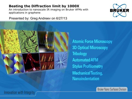
Beating <strong>the</strong> Diffraction limit by 1000XAn introduction to nanoscale IR imaging on <strong>Bruker</strong> AFMs withapplications in graphenePresented by: Greg Andreev on 6/27/13
Why do people use Infrared Spectroscopy?Main reason: it allows chemical identificationExample IR spectrumPMMA polymerDuan G. et. al. Nanoscale Res. Lett. (2008)Absorption resonances = Unique IR fingerprint6/27/13 <strong>Bruker</strong> Nano Surfaces3
Why Infrared sSNOM at <strong>the</strong> Nanoscale?Characterization and IdentificationPolymersSemiconductors7.5um x 7.5um7.5umM. Raschke et. al. ChemPhysChem 2005 A.J. Huber et. al. NanoLett 200850nm x 50nmBiology: Tobacco Mosaic Virus50nm x 50nmBiology: Human Tooth Dentin100nm50nm x 50nmM. Brehm et. al. NanoLett 2006G.O. Andreev – 2011, unpublished6/27/13 <strong>Bruker</strong> Nano Surfaces 4a
Why Infrared sSNOM at <strong>the</strong> Nanoscale?Characterization and IdentificationPolymersSemiconductors50nm x 50nmBiology: Tobacco Mosaic Virus~2um Spot7.5um x 7.5um50nm x 50nm7.5umM. Raschke et. al. ChemPhysChem 2005 A.J. Huber et. al. NanoLett 2008Biology: Human Tooth Dentin100nm50nm x 50nmM. Brehm et. al. NanoLett 20066/27/13 <strong>Bruker</strong> Nano SurfacesG.O. Andreev – 2011, unpublished4b
Just how big is a 1000X improvement inresolution?Far field IR imagePaintNear field IR imageStitchingmaterialGrassBall1000XzoomSoilcompound IR can ID main features of <strong>the</strong>soccer field× Resolution is limited Nanoscale IR can ID <strong>the</strong>most subtle features Resolution is 1000X betterTo make this transition we need to beat <strong>the</strong> diffraction limit6/27/13 <strong>Bruker</strong> Nano Surfaces5
Resolution limit in Far field opticsFar field imaging system:zxk ⊥k ∥We sample <strong>the</strong> object usingplane waves:2π/k ∥λk ||2π/λ = k ∥ 2 + k ⊥2Lensk ∥,max = 2π sin θ/λθkNyquistSampled dd min = λ2sin θTwo objectsto resolveFar field optics limits IR resolution to λ , or several μm6/27/13 <strong>Bruker</strong> Nano Surfaces6
Resolution limit in near field opticsNear field imagingsystem:zxaPoint sourcedIn <strong>the</strong> near field, a ≪ λSample w/two objectsWe sample <strong>the</strong> object using many evanescent wavese +ik ∥xe −ik ∥xk ⊥k ∥+ all possible k ||e −k ∥zNow have access to imaginary k ⊥ !2π/λ = k ∥ 2 + k ⊥2k ∥,max ~2π/ad min ~a/2Largest k ∥ ≫ 2π/λk ⊥ ~ik ∥For near field optics, resolution islimited only by distance to source6/27/13 <strong>Bruker</strong> Nano Surfaces7
How do we create such a point source?We use sSNOM: scattering Scanning Near-field Optical Microscopy~20nmLightning rod principle100nm• Shining IR light on AFM tip polarizes <strong>the</strong> apex (Lightning rod effect)• The apex turns into an IR point source ~ 10nm away from surface (tip radius)• Detection: scattered light transfers near field info to far fieldTip radius determines IR resolution = 10nm resolution6/27/13 <strong>Bruker</strong> Nano Surfaces8
Optical contrast in sSNOM for 3D and 2Dmaterials: it works for both!3DEffect of sample:-p t+--p t++Larger Reflection---p t+++Insulating ConductingResonant2DEffect of sample:-p t+---p t+++Larger ReflectionNon-resonantResonant6/27/13 <strong>Bruker</strong> Nano Surfaces9
Experimental Implementation6/27/13 <strong>Bruker</strong> Nano Surfaces10
How <strong>the</strong> near field light (E nf ) is detected:Background Suppression andInterferometric DetectionsSNOM schematic:MM = moving mirrorPM = parabolic mirrorBS = beam splitterMCT = HgCdTe IR detectorE refE nf +E bgDetector Voltage: V det ∝ EE ∗ = |E ref +E nf +E bg | 2Goals of <strong>the</strong> detection scheme:1. Suppress <strong>the</strong> background, E bg , contributions to detector voltage V det2. Perform a phase sensitive measurement of E nf6/27/13 <strong>Bruker</strong> Nano Surfaces11
How <strong>the</strong> near field light (E nf ) is detected:Background Suppression andInterferometric DetectionTapping mode:E bgE nf +E bgsSNOM schematic:MM = moving mirrorPM = parabolic mirrorBS = beam splitterMCT = HgCdTe IR detectorE refE nf +E bgDetector Voltage: V det ∝ EE ∗ = |E ref +E nf +E bg | 2∝ E ref E nf cos φ ref − φ nf + E bg E nf cos φ bg − φ nf + E ref E bg cos φ ref − φ bgDesired termSuppressed terms:+ E ref2+ |E nf | 2 + |E bg | 26/27/13 <strong>Bruker</strong> Nano Surfaces12
sSNOM results from customers:implementation on <strong>Bruker</strong> AFMplatforms6/27/13 <strong>Bruker</strong> Nano Surfaces13
University of Colorado at Boulder(Prof. Raschke Lab)ParabolicMirrorMCT IR Detector,Liquid nitrogen cooledPiezo actuated mirrorXYZ stageIRBeamsplitter<strong>Bruker</strong>Innova*Parabolic Mirror,~0.4NA effective*Innova Head removed to allow greatervisibility of Parabolic Mirror6/27/13 <strong>Bruker</strong> Nano Surfaces14
University of Toronto – Prof. Walker labSpectroscopic NanoImaging of Boron Nitride nanotubes<strong>Bruker</strong>Multimode• Nanoscale intra-nanotube inhomogeneityrevealed• IR sSNOM spectra show contrasts over aslittle as 20nm• Rich in information, beyond FTIR absorptionXu, X. G.; Tanur, A. E.; Walker, G. C. The Journal of Physical Chemistry A 2013, 117, 3348.6/27/13 <strong>Bruker</strong> Nano Surfaces16
sSNOM results from <strong>Bruker</strong> Nano on a2D material: Graphene6/27/13 <strong>Bruker</strong> Nano Surfaces17
IntroductionGraphene Discovery, with <strong>Bruker</strong> AFM• The Nobel Prize in Physics 2010was awarded jointly to Andre Geimand Konstantin Novoselov (Univ. ofManchester)"for groundbreaking experimentsregarding <strong>the</strong> two-dimensional materialgraphene"• http://www.nobelprize.org/nobel_prizes/physics/laureates/2010/#Andre Geim© The Nobel FoundationKonstantin Novoselov© The Nobel Foundation© The Nobel FoundationMultiMode• Identification by optical survey(phase contrast) followed by AFM:“AFM is currently <strong>the</strong> only method thatallows definitive identification of singlelayercrystals”• Novoselov et al. PNAS 102 (30), 10451-3, 2005Identifying single layers by AFM:(a) NbSe 2 and (b) Graphene.Novoselov et al. PNAS 102 (30), 10451-3, 2056/27/13 <strong>Bruker</strong> Nano Surfaces18
IntroductionWhat Is Graphene And Why Do We Care?• Graphene = one-atom-thick sheet of (sp2-bonded) carbon atoms• Like 1 layer in graphite• 2D material = new class of materials• Lots of Superlatives:• Thinnest material (1 atomic layer)• Largest surface area (2700sqm/g)• Strongest material ‘ever measured’ (<strong>the</strong>oretical limit)• Stiffest known material (stiffer than diamond)• Most stretchable material (20% elastically)• Record <strong>the</strong>rmal conductivity (outperforming diamond)• Highest current density at RT (10^6 x Cu)• Completely impermeable (even to He)• Highest intrinsic mobility (100x Si)• Conducts electricity in <strong>the</strong> limit of no electrons• Lightest charge carriers (zero rest mass)• Longest mean free path at RT6/27/13 <strong>Bruker</strong> Nano Surfaces19
Infrared study of Graphene: rich spectrumallows access to key observablesIR optical conductivity:2E f ±ΓYields info about:Im(σ)Re(σ)DrudeConductivityUniversalConductivityCarrier DensityDefectsSubstrate Effectsetc…E f = 650cm -1 , Γ = 30cm -1N. M. R. Peres et. al, EPL, (2008)Z.Q. Li et. al., Nature Phys, (2008)6/27/13 <strong>Bruker</strong> Nano Surfaces20
sSNOM IR study of Graphene: same richspectrum PLUS plasmonicsNear fieldspectrum2E f ±ΓFar fieldSpectrumPlasmonicsUniversalConductivityNear field spectrum yields same info as far field: Fermi energy, scattering rateBUT also shows a plasmonic resonance – not present in far field6/27/13 <strong>Bruker</strong> Nano Surfaces21
Let’s probe Graphene’s universalconductivity at <strong>the</strong> nanoscalePlasmonicsUniversalConductivityIR frequency6/27/13<strong>Bruker</strong> Nano Surfaces22
<strong>Bruker</strong> solutions for Graphene research:TERS, colocalized Raman, PeakForce KPFM, QNMand now sSNOMIcon RamanCatalyst IRISInnova IRIS6/27/13 <strong>Bruker</strong> Nano Surfaces23
Colocalized SPM investigation ofGraphene: Mechanical, Electrical, OpticalAFM G-band Raman D-band RamanConfirmed n+1 layer Confirmed 1,2,3,4 layers ID defects, confirm n=1PF KPFM80mVUpper Limit on E fIR 1730cm -1Measure σ(ω)Graphene Applications:• AFM: layer heights,mechanical properties• Raman: how manylayers, defects• PF KPFM: workfunction/Fermi energy• IR: plasmonics, # oflayers, Fermi energy6/27/13 <strong>Bruker</strong> Nano Surfaces24
sSNOM in universal conductivity regime:layer counting and unexpected resultsIR 1730cm -1 • Expected: contrast consistent withUniversal Conductivity• Confirmed |σ 4 |>|σ 3 |>|σ 2 |>|σ 1 | for ω>2E f• Reproducible – useful for layer counting• Unexpected results:• 1L < SiO 2• Huge jump from 3L to 4LTheoretical PredictionωWhy lower??SiO 212342E f6/27/13<strong>Bruker</strong> Nano Surfaces2625
sSNOM in universal conductivity regime:Sensitivity to defectsLet’s zoom in..D-band RamanIR 1730cm -16/27/13 <strong>Bruker</strong> Nano Surfaces26
Remarkable sensitivity: sSNOM imagesshow fine contrasts due to defectsNanomechanics shows signs of wrinklessSNOM confirms0.199±0.0007Hint of defectsin Dband Raman0.203±0.0004Easily detectable ~2% contrast6/27/13 <strong>Bruker</strong> Nano Surfaces27
Now let’s switch to <strong>the</strong> plasmonicregimePlasmonicsUniversalConductivityIR frequency6/27/13<strong>Bruker</strong> Nano Surfaces28
sSNOM of Graphene in <strong>the</strong> PlasmonicRegime: launching and imagingIR 1730cm -1 IR 870cm -1• Plasmon clearly observed in Single layer Graphene• Origin: waves launched by tip reflecting back to tip296/27/13 <strong>Bruker</strong> Nano Surfaces
sSNOM of Graphene: fast imaging ofplasmons~140nm• 10Hz image obtained injust 60s• No significant loss ofspatial resolution1Hz 4Hz 10HzsSNOM on a <strong>Bruker</strong> AFMis fast without any loss inresolution6/27/13 <strong>Bruker</strong> Nano Surfaces30
How important is <strong>the</strong> spatial frequency forGraphene plasmonics?Dull Tip = low k || Fresh Tip = large k ||k ∥,max < k SPk ∥,max ~k SPSharper tips have larger in-plane momenta – a necessity for plasmonics6/27/13 <strong>Bruker</strong> Nano Surfaces31
Conclusion• Near field imaging with sSNOM is powerful and unique• 10nm resolution – 1000X better than far field IR• Remarkable sensitivity to ultrathin materials• Access to nanoplasmonics• New results• First nanoscale IR images of Graphene’s Universal Conductivity• Fastest images yet of a nanoplasmonFor more info please contact Greg Andreev: gregory.andreev@bruker-nano.com6/27/13 <strong>Bruker</strong> Nano Surfaces32