TA8403K - Unitrel
TA8403K - Unitrel
TA8403K - Unitrel

Create successful ePaper yourself
Turn your PDF publications into a flip-book with our unique Google optimized e-Paper software.
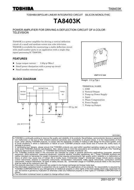
TOSHIBA BIPOLAR LINEAR INTEGRATED CIRCUIT SILICON MONOLITHIC<strong>TA8403K</strong><strong>TA8403K</strong>POWER AMPLIFIER FOR DRIVING A DEFLECTION CIRCUIT OF A COLORTELEVISION<strong>TA8403K</strong> is a power amplifier for driving a vertical deflectioncircuit of a small and medium screen size color television.<strong>TA8403K</strong> is available for constructing a stable deflection circuitwith small number parts in an application with a single chipsignal processing IC TA8879N.FEATURESLarge output current : 1.8Ap-p (Max.)Small power dissipation with a pump-up circuitSmall number external partsBLOCK DIAGRAMWeight : 2.2 g (Typ.)TERMINAL NAME1. GND2. Vertical Output3. Pump-up Power Supply4. Input5. Phase Compensation6. Power Supply7. Pump-up Output000707EBA1TOSHIBA is continually working to improve the quality and reliability of its products. Nevertheless, semiconductor devices in generalcan malfunction or fail due to their inherent electrical sensitivity and vulnerability to physical stress. It is the responsibility of thebuyer, when utilizing TOSHIBA products, to comply with the standards of safety in making a safe design for the entire system, andto avoid situations in which a malfunction or failure of such TOSHIBA products could cause loss of human life, bodily injury ordamage to property.In developing your designs, please ensure that TOSHIBA products are used within specified operating ranges as set forth in themost recent TOSHIBA products specifications. Also, please keep in mind the precautions and conditions set forth in the “HandlingGuide for Semiconductor Devices,” or “TOSHIBA Semiconductor Reliability Handbook” etc..The TOSHIBA products listed in this document are intended for usage in general electronics applications (computer, personalequipment, office equipment, measuring equipment, industrial robotics, domestic appliances, etc.). These TOSHIBA products areneither intended nor warranted for usage in equipment that requires extraordinarily high quality and/or reliability or a malfunction orfailure of which may cause loss of human life or bodily injury (“Unintended Usage”). Unintended Usage include atomic energycontrol instruments, airplane or spaceship instruments, transportation instruments, traffic signal instruments, combustion controlinstruments, medical instruments, all types of safety devices, etc.. Unintended Usage of TOSHIBA products listed in this documentshall be made at the customer’s own risk.The products described in this document are subject to the foreign exchange and foreign trade laws.The information contained herein is presented only as a guide for the applications of our products. No responsibility is assumed byTOSHIBA CORPORATION for any infringements of intellectual property or other rights of the third parties which may result from itsuse. No license is granted by implication or otherwise under any intellectual property or other rights of TOSHIBA CORPORATION orothers.The information contained herein is subject to change without notice.2001-02-07 1/5
<strong>TA8403K</strong>MAXIMUM RATINGS (Ta = 25°C)CHARACTERISTIC SYMBOL RATING UNITPower Supply Voltage VCC 30 VPump-up Power Supply Voltage VVt 60 VTerminal VoltageEinGND −0.3 ~VVt +0.3VInput Signal Voltage ein 0~1.2 VPower Dissipation PD 15 (Note) WOperating Temperature Topr −20~85 °CStorage Temperature Tstg −55~150 °CNote:Using an infinite heat sinkRECOMMENDED OPERATING CONDITIONCHARACTERISTIC SYMBOL MIN. TYP. MAX. UNITPower Supply VCC — 24 27 VDeflection Output Current I2p-p — — 1.8 Ap-p2001-02-07 2/5
<strong>TA8403K</strong>ELECTRICAL CHARACTERISTICS (Ta = 25°C, V CC = 24V)CHARACTERISTICSaturation Voltage of the VerticalOutput Transistor (1)Saturation Voltage of the VerticalOutput Transistor (2)Saturation Voltage of the Pump-upOutput Transistor (1)Saturation Voltage of the Pump-upOutput Transistor (2)SYMBOLTESTCIR-CUITTEST CONDITION MIN. TYP. MAX. UNITVv (sat) 1 1 Note 1: 0.3 0.5 1.0 VVv (sat) 2 1 Note 2: 1.0 1.8 3.6 VVp (sat) 1 1 Note 3: 1.0 2.0 3.0 VVp (sat) 2 1 Note 4: 0.3 0.8 1.6 VOutput Current with no input Ib 10.0 15.0 30.0 mA1 Note 5:Center Output VoltageVcenter10.0 12.0 14.0 VNote 1: SW 1 : ON, SW 2 : C, SW 3 : ON, SW 4 : B, SW 5 : A, SW 6 : AMeasure the voltage of pin2.Note 2: SW 1 : ON, SW 2 : C, SW 3 : ON, SW 4 : A, SW 5 : A, SW 6 : BMeasure the voltage of pin2, V 2 . V V (sat) 2 = V CC − V 2Note 3: SW 1 : ON, SW 2 : B, SW 3 : OFF, SW 4 : A, SW 5 : C, SW 6 : AMeasure the voltage of pin7, V 7 . V P (sat) 1 = V CC − V 7Note 4: SW 1 : OFF, SW 2 : C, SW 3 : OFF, SW 4 : A, SW 5 : B, SW 6 : BMeasure the voltage of pin7.Note 5: SW 1 : ON, SW 2 : A, SW 3 : ON, SW 4 : C, SW 5 : A, SW 6 : BMeasure the sink current into pin3.Measure the voltage of pin2.Note 6: <strong>TA8403K</strong> is checked its output wave form in a real operating circuit.2001-02-07 3/5
<strong>TA8403K</strong>TEST CIRCUIT 1APPLICATION EXAMPLE CIRCUIT2001-02-07 4/5
<strong>TA8403K</strong>PACKAGE DIMENSIONSWeight: 2.2 g (Typ.)2001-02-07 5/5