WM8726, Rev 4.8 - Wolfson Microelectronics plc
WM8726, Rev 4.8 - Wolfson Microelectronics plc
WM8726, Rev 4.8 - Wolfson Microelectronics plc

You also want an ePaper? Increase the reach of your titles
YUMPU automatically turns print PDFs into web optimized ePapers that Google loves.
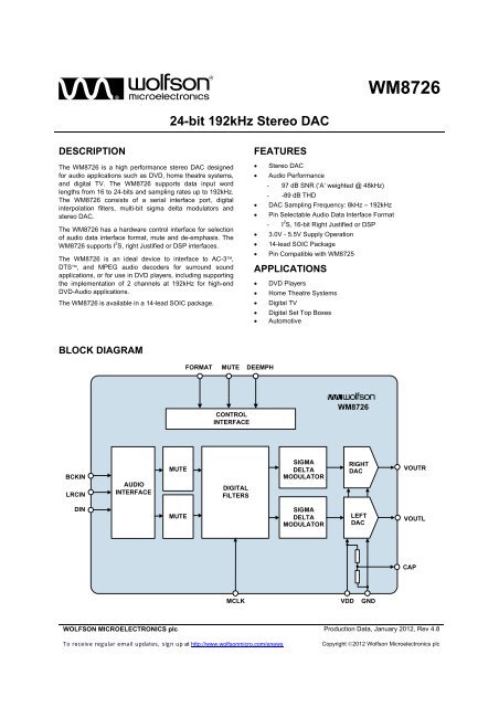
<strong>WM8726</strong>Production DataPIN DESCRIPTIONPIN NAME TYPE DESCRIPTION1 LRCIN Digital input Sample rate clock input2 DIN Digital input Serial audio data input3 BCKIN Digital input Bit clock input4 NC No connect No internal connection5 CAP Analogue output Analogue internal reference6 VOUTR Analogue output Right channel DAC output7 GND Supply Negative supply8 VDD Supply Positive supply9 VOUTL Analogue output Left channel DAC output10 MUTE Digital input Soft mute control, Internal pull downHigh Impedance = AutomuteHigh = Mute ONLow = Mute OFF11 NC No connect No internal connection12 DEEMPH Digital input De-emphasis select, Internal pull upHigh = de-emphasis ONLow = de-emphasis OFF13 FORMAT Digital input Data input format select, Internal pull upLow = 16-bit right justified or DSP ‘late’High = 16-24-bit I 2 S or DSP ‘early’14 MCLK Digital input Master clock inputNote:1. Digital input pins have Schmitt trigger input buffers.wPD, <strong>Rev</strong> <strong>4.8</strong>, January 20124
<strong>WM8726</strong>Production DataABSOLUTE MAXIMUM RATINGSAbsolute Maximum Ratings are stress ratings only. Permanent damage to the device may be caused by continuously operating ator beyond these limits. Device functional operating limits and guaranteed performance specifications are given under ElectricalCharacteristics at the test conditions specified.ESD Sensitive Device. This device is manufactured on a CMOS process. It is therefore generically susceptibleto damage from excessive static voltages. Proper ESD precautions must be taken during handling and storageof this device.<strong>Wolfson</strong> tests its package types according to IPC/JEDEC J-STD-020B for Moisture Sensitivity to determine acceptable storageconditions prior to surface mount assembly. These levels are:MSL1 = unlimited floor life at
<strong>WM8726</strong>Production DataDC ELECTRICAL CHARACTERISTICSPARAMETER SYMBOL TEST CONDITIONS MIN TYP MAX UNITSupply range VDD 3.0 5.5 VGround GND 0 VSupply current VDD = 5V 27 mASupply current VDD = 3.3V 23 mAPower down current (note 4) VDD=3.3V 0.6 mAELECTRICAL CHARACTERISTICSAll MIN/MAX characteristics are guaranteed over the recommended operating conditions. Typical characteristics are based onmeasurements taken under the test conditions specified below.Test ConditionsVDD = 5V, GND = 0V, T A = +25 o C, fs = 48kHz, MCLK = 256fs unless otherwise stated.PARAMETER SYMBOL TEST CONDITIONS MIN TYP MAX UNITDigital Logic Levels (TTL Levels)Input LOW level V IL 0.8 VInput HIGH level V IH 2.0 VOutput LOW V OL I OL = 2mA GND + 0.3V VOutput HIGH V OH I OH = 2mA VDD - 0.3V VAnalogue Reference LevelsReference voltage (CAP) VDD/2 VPotential divider resistance R CAP VDD to CAP and CAPto GNDDAC Output (Load = 10k 50pF)0dBFs Full scale output voltage At DAC outputs 1.1 xVDD/5DAC Performance (+25˚C )SNR (Note 1,2,3)A-weighted,90 97 dB@ fs = 48kHzSNR (Note 1,2,3)A-weighted94 dB@ fs = 96kHzSNR (Note 1,2,3)A-weighted94 dB@ fs = 192kHzSNR (Note 1,2,3)A-weighted,93 dB@ fs = 48kHzVDD = 3.3VSNR (Note 1,2,3)A-weighted93 dB@ fs = 96kHzVDD = 3.3VSNR (Note 1,2,3) Non ‘A’ weighted @ fs =95 dB48kHzTHD (Note 3) 1kHz, 0dBFs -89 dBDynamic Range (Note 2)1kHz, THD+N @ 90 97 dB-60dBFsDAC channel separation 93 dBAnalogue Output LevelsOutput level Load = 10k, 0dBFS 1.1 V RMSLoad = 10k, 0dBFS,0.72 V RMS(VDD = 3.3V)33kV rmswPD, <strong>Rev</strong> <strong>4.8</strong>, January 20126
<strong>WM8726</strong>Production DataTest ConditionsVDD = 5V, GND = 0V, T A = +25 o C, fs = 48kHz, MCLK = 256fs unless otherwise stated.PARAMETER SYMBOL TEST CONDITIONS MIN TYP MAX UNITGain mismatchchannel-to-channel±1 %FSRMinimum resistance loadTo midrail or a.c.1 kcoupledTo midrail or a.c.1 kcoupled(VDD = 3.3V)Maximum capacitance load 5V or 3.3V 100 pFOutput d.c. level VDD/2 VPower On Reset (POR)POR threshold 2.4 VNotes:1. Ratio of output level with 1kHz full scale input, to the output level with all zeros into the digital input, measured ‘A’ weightedover a 20Hz to 20kHz bandwidth.2. All performance measurements done with 20kHz low pass filter, and where noted an A-weight filter. Failure to use such afilter will result in higher THD+N and lower SNR and Dynamic Range readings than are found in the ElectricalCharacteristics. The low pass filter removes out of band noise; although it is not audible it may affect dynamic specificationvalues.3. CAP pin decoupled with 10uF and 0.1uF capacitors (smaller values may result in reduced performance).4. Power down occurs 1.5s after MCLK is stopped.TERMINOLOGY1. Signal-to-noise ratio (dB) - SNR is a measure of the difference in level between the full scale output and the output with nosignal applied. (No Auto-zero or Automute function is employed in achieving these results).2. Dynamic range (dB) - DNR is a measure of the difference between the highest and lowest portions of a signal. Normally aTHD+N measurement at 60dB below full scale. The measured signal is then corrected by adding the 60dB to it. (e.g.THD+N @ -60dB= -32dB, DR= 92dB).3. THD+N (dB) - THD+N is a ratio, of the rms values, of (Noise + Distortion)/Signal.4. Stop band attenuation (dB) - Is the degree to which the frequency spectrum is attenuated (outside audio band).5. Channel Separation (dB) - Also known as Cross-Talk. This is a measure of the amount one channel is isolated from theother. Normally measured by sending a full scale signal down one channel and measuring the other.wPD, <strong>Rev</strong> <strong>4.8</strong>, January 20127
<strong>WM8726</strong>Production DataMASTER CLOCK TIMINGt MCLKLMCLKt MCLKHt MCLKYFigure 1 Master Clock Timing RequirementsTest ConditionsVDD = 5V, GND = 0V, T A = +25 o C, fs = 48kHz, MCLK = 256fs unless otherwise stated.PARAMETER SYMBOL TEST CONDITIONS MIN TYP MAX UNITSystem Clock Timing InformationMCLK Master clock pulse width high t MCLKH 8 nsMCLK Master clock pulse width low t MCLKL 8 nsMCLK Master clock cycle time t MCLKY 20 nsMCLK Duty cycle 40:60 60:40Time from MCLK stopping to powerdown.1.5 12 sDIGITAL AUDIO INTERFACEt BCHt BCLBCKINt BCYLRCINt DSt LRSUt LRHt DHDINFigure 2 Digital Audio Data TimingTest ConditionsVDD = 5V, GND = 0V, T A = +25 o C, fs = 48kHz, MCLK = 256fs unless otherwise stated.PARAMETER SYMBOL TEST CONDITIONS MIN TYP MAX UNITAudio Data Input Timing InformationBCKIN cycle time t BCY 40 nsBCKIN pulse width high t BCH 16 nsBCKIN pulse width low t BCL 16 nsLRCIN set-up time to BCKINrising edgeLRCIN hold time fromBCKIN rising edgeDIN set-up time to BCKINrising edgeDIN hold time from BCKINrising edget LRSU 8 nst LRH 8 nst DS 8 nst DH 8 nswPD, <strong>Rev</strong> <strong>4.8</strong>, January 20128
<strong>WM8726</strong>POWER ON RESET (POR)Production DataThe <strong>WM8726</strong> has an internal power-on-reset (POR) circuit which is used to reset the digital logicinto a default state after power up. A block diagram of the reset circuit is shown in Figure 3Figure 3 Block Diagram of Power-On-ResetThe active low reset signal NPOR will be asserted low until VDD=2.4V, which means VMID risesto 1.2V. When this threshold has been reached, then the NPOR is released and the digitalinterface has been reset. This is illustrated in the diagram shown in Figure 4.Figure 4 Generation of Internal NPOR at Power-On-ResetwPD, <strong>Rev</strong> <strong>4.8</strong>, January 20129
<strong>WM8726</strong>Production DataFigure 5 illustrates the NPOR generation when the power is removed.Figure 5 Generation of NPOR at Power-Off-ResetwPD, <strong>Rev</strong> <strong>4.8</strong>, January 201210
<strong>WM8726</strong>Production Data1/fsLEFT CHANNELRIGHT CHANNELLRCINBCKIN1 BCKIN1 BCKINDIN1 2 3n-2 n-1n1 2 3n-2 n-1nMSBLSBMSBLSBFigure 6 I 2 S Mode Timing DiagramRIGHT JUSTIFIED MODEThe <strong>WM8726</strong> supports word lengths of 16-bits in right justified mode.In right justified mode, the digital audio interface receives data on the DIN input. Audio Data is timemultiplexed with LRCIN indicating whether the left or right channel is present. LRCIN is also usedas a timing reference to indicate the beginning or end of the data words.In right justified mode, the minimum number of BCKINs per LRCIN period is 2 times the selectedword length. LRCIN must be high for a minimum of word length BCKINs and low for a minimum ofword length BCKINs. Any mark to space ratio on LRCIN is acceptable provided the aboverequirements are met.In right justified mode, the LSB is sampled on the rising edge of BCKIN preceding a LRCINtransition. LRCIN is high during the left samples and low during the right samples.1/fsLEFT CHANNELRIGHT CHANNELLRCINBCKINDIN1 2 314 15161 2 314 1516MSBLSBMSBLSBFigure 7 Right Justified Mode Timing DiagramDSP MODEA DSP compatible, time division multiplexed format is also supported by the <strong>WM8726</strong>. This formatis of the type where a ‘synch’ pulse is followed by two data words (left and right) of predeterminedword length. (16-bits). The ‘synch’ pulse replaces the normal duration LRCIN, and DSP mode isauto-detected by the shorter than normal duration of the LRCIN. If LRCIN is of 4 BCKIN or lessduration, the DSP compatible format is selected. Mode A and Mode B clock formats aresupported, selected by the state of the FORMAT pin.wPD, <strong>Rev</strong> <strong>4.8</strong>, January 201213
<strong>WM8726</strong>Production DataA diagram showing how the various Mute modes interact is shown below in Figure 11.AUTOMUTED(Internal Signal)MUTEPIN10kSOFTMUTE(Internal Signal)Figure 11 Selection Logic for MUTE ModesINPUT AUDIO FORMAT SELECTIONFORMAT (pin 13) controls the data input format.FORMATINPUT DATA MODE0 16 bit right justified1 16–24 bit I 2 STable 3 Input Audio Format SelectionNotes:1. In 16-24 bit I 2 S mode, any data from 16-24 bits or more is supported provided that LRCIN ishigh for a minimum of data width BCKINs and low for a minimum of data width BCKINs,unless Note 2. For data widths greater than 24 bits, the LSB’s will be truncated and the mostsignificant 24 bits will be used by the internal processing.2. If exactly 16 BCKIN cycles occur in both the low and high period of LRCIN the <strong>WM8726</strong> willassume the data is 16-bit and accept the data accordingly.INPUT DSP FORMAT SELECTIONFORMAT 50% LRCIN DUTY CYCLE LRCIN of 4 BCKIN or Less Duration0 16 bit(MSB-first, right justified)1 I 2 S format up to 24 bit(Philips serial data protocol)Table 4 DSP Interface FormatsDSP format – ‘late’ modeDSP format – ‘early’ modeDE-EMPHASIS CONTROLDEM (pin 12) is an input control for selection of de-emphasis filtering to be applied.DEEMPHDE-EMPHASIS0 Off1 OnTable 5 De-emphasis ControlDAC OUTPUT PHASEIn the DAC to analogue output, the analogue output data VOUTL/R, is a phase inverted representation ofthe digital input signal.wPD, <strong>Rev</strong> <strong>4.8</strong>, January 201216
<strong>WM8726</strong>Production DataDIGITAL FILTER CHARACTERISTICSPARAMETER SYMBOL TEST CONDITIONS MIN TYP MAX UNITPassband Edge -3dB 0.487fsPassband Ripple f < 0.444fs 0.05 dBStopband Attenuation f > 0.555fs -60 dBTable 6 Digital Filter CharacteristicsDAC FILTER RESPONSES0.200.15-200.1Response (dB)-40-60-80Response (dB)0.050-0.05-0.1-100-0.15-1200 0.5 1 1.5 2 2.5 3Frequency (Fs)-0.20 0.05 0.1 0.15 0.2 0.25 0.3 0.35 0.4 0.45 0.5Frequency (Fs)Figure 12 DAC Digital Filter Frequency Response-44.1, 48 and 96kHz0Figure 13 DAC Digital Filter Ripple-44.1, 48 and 96kHz0.20-20-0.2Response (dB)-40-60Response (dB)-0.4-0.6-0.8-800 0.2 0.4 0.6 0.8 1Frequency (Fs)Figure 14 DAC Digital Filter Frequency Response -192kHz-10 0.05 0.1 0.15 0.2 0.25 0.3 0.35 0.4 0.45 0.5Frequency (Fs)Figure 15 DAC Digital Filter Ripple -192kHzwPD, <strong>Rev</strong> <strong>4.8</strong>, January 201217
<strong>WM8726</strong>Production DataDIGITAL DE-EMPHASIS CHARACTERISTICS010.5-20Response (dB)-4-6Response (dB)-0.5-1-1.5-8-2-2.5-100 2 4 6 8 10 12 14 16Frequency (kHz)-30 2 4 6 8 10 12 14 16Frequency (kHz)Figure 16 De-Emphasis Frequency Response (32kHz)0Figure 17 De-Emphasis Error (32kHz)0.4-20.30.2Response (dB)-4-6Response (dB)0.10-0.1-8-0.2-0.3-100 5 10 15 20Frequency (kHz)-0.40 5 10 15 20Frequency (kHz)Figure 18 De-Emphasis Frequency Response (44.1kHz)0Figure 19 De-Emphasis Error (44.1kHz)10.8-20.60.4Response (dB)-4-6Response (dB)0.20-0.2-0.4-8-0.6-0.8-100 5 10 15 20Frequency (kHz)-10 5 10 15 20Frequency (kHz)Figure 20 De-Emphasis Frequency Response (48kHz)Figure 21 De-Emphasis Error (48kHz)wPD, <strong>Rev</strong> <strong>4.8</strong>, January 201218
<strong>WM8726</strong>Production DataAPPLICATIONS INFORMATIONRECOMMENDED EXTERNAL COMPONENTSVDD+C 1 C 287VDDGNDAGND13 FORMATHardware Control12 DEEMPHVOUTR10 MUTE6<strong>WM8726</strong>VOUTL9C 3+ +C 4AC-CoupledVOUTR/Lto External LPF1 LRCINAudio Serial Data I/F14 MCLK3 BCKIN2 DINCAP5+C 5C 6AGNDNotes:1. C2, C5 should be positioned as close to the <strong>WM8726</strong> as possible.2. Capacitor types should be carefully chosen. Capacitors with very low ESR arerecommended for optimum performance.3. C3 and C4 not required if using the recommended low pass filter in Figure 20.Figure 22 External Component DiagramRECOMMENDED EXTERNAL COMPONENTS VALUESCOMPONENTREFERENCESUGGESTEDVALUEC1 10F De-coupling for VDDC2 0.1F De-coupling for VDDDESCRIPTIONC3 and C4 10F Output AC coupling caps to remove midrail DC level from outputsC5 0.1F Reference de-coupling capacitors for CAP pinC610FTable 7 External Components DescriptionwPD, <strong>Rev</strong> <strong>4.8</strong>, January 201219
<strong>WM8726</strong>RECOMMENDED ANALOGUE LOW PASS FILTERProduction Data4.7k4.7k+VS+10uF1.8k7.5K_+5147k1.0nF680pF-VSFigure 23 Recommended 2 nd Order Low Pass FilterAn external low pass filter is recommended (see Figure 20) if the device is driving a widebandamplifier. In some applications, a passive RC filter may be adequate.PCB LAYOUT RECOMMENDATIONSCare should be taken in the layout of the PCB that the <strong>WM8726</strong> is to be mounted to. Thefollowing notes will help in this respect:1. The VDD supply to the device should be as noise free as possible. This can beaccomplished to a large degree with a 10uF bulk capacitor placed locally to the device and a0.1uF high frequency decoupling capacitor placed as close to the VDD pin as possible. It isbest to place the 0.1uF capacitor directly between the VDD and GND pins of the device onthe same layer to minimize track inductance and thus improve device decouplingeffectiveness.2. The CAP pin should be as noise free as possible. This pin provides the decoupling forthe on chip reference circuits and thus any noise present on this pin will be directly coupledto the device outputs. In a similar manner to the VDD decoupling described in 1. above, thispin should be decoupled with a 10uF bulk capacitor local to the device and a 0.1uF capacitoras close to the CAP pin as possible.3. Separate analogue and digital track routing from each other. The device is split intoanalogue (pins 5 – 9) and digital (pins 1 – 4 & pins 10 – 14) sections that allow the routing ofthese signals to be easily separated. By physically separating analogue and digital signals,crosstalk from the PCB can be minimized.4. Use an unbroken solid GND plane. To achieve best performance from the device, it isadvisable to have either a GND plane layer on a multilayer PCB or to dedicate one side of a2 layer PCB to be a GND plane. For double sided implementations it is best to route asmany signals as possible on the device mounted side of the board, with the opposite sideacting as a GND plane. The use of a GND plane greatly reduces any electrical emissionsfrom the PCB and minimizes crosstalk between signals.An evaluation board is available for the <strong>WM8726</strong> that demonstrates the above techniques and theexcellent performance achievable from the device. This can be ordered or the User manualdownloaded from the <strong>Wolfson</strong> web site at www.wolfsonmicro.comwPD, <strong>Rev</strong> <strong>4.8</strong>, January 201220
<strong>WM8726</strong>PACKAGE DIMENSIONSD: 14 PIN SOIC 3.9mm Wide BodyProduction DataDM001.CeB148HE17DLh x 45 o-C-A1SEATING PLANEA0.10 (0.004)CSymbolsDimensions(mm)Dimensions(Inches)MIN MAX MIN MAXA 1.35 1.75 0.0532 0.0688A1 0.10 0.25 0.0040 0.0098B 0.33 0.51 0.0130 0.0200C 0.19 0.25 0.0075 0.0098D 8.55 8.75 0.3367 0.3444E 3.80 4.00 0.1497 0.1574e 1.27 BSC 0.05 BSCH 5.80 6.20 0.2284 0.2440h 0.25 0.50 0.0099 0.0196L 0.40 1.27 0.0160 0.0500 0 o 8 o 0 o 8 oREF:JEDEC.95, MS-012NOTES:A. ALL LINEAR DIMENSIONS ARE IN MILLIMETERS (INCHES).B. THIS DRAWING IS SUBJECT TO CHANGE WITHOUT NOTICE.C. BODY DIMENSIONS DO NOT INCLUDE MOLD FLASH OR PROTRUSION, NOT TO EXCEED 0.25MM (0.010IN).D. MEETS JEDEC.95 MS-012, VARIATION = AB. REFER TO THIS SPECIFICATION FOR FURTHER DETAILS.wPD, <strong>Rev</strong> <strong>4.8</strong>, January 201221
<strong>WM8726</strong>Production DataIMPORTANT NOTICE<strong>Wolfson</strong> <strong>Microelectronics</strong> <strong>plc</strong> (“<strong>Wolfson</strong>”) products and services are sold subject to <strong>Wolfson</strong>’s terms and conditions of sale,delivery and payment supplied at the time of order acknowledgement.<strong>Wolfson</strong> warrants performance of its products to the specifications in effect at the date of shipment. <strong>Wolfson</strong> reserves the right tomake changes to its products and specifications or to discontinue any product or service without notice. Customers shouldtherefore obtain the latest version of relevant information from <strong>Wolfson</strong> to verify that the information is current.Testing and other quality control techniques are utilised to the extent <strong>Wolfson</strong> deems necessary to support its warranty. Specifictesting of all parameters of each device is not necessarily performed unless required by law or regulation.In order to minimise risks associated with customer applications, the customer must use adequate design and operatingsafeguards to minimise inherent or procedural hazards. <strong>Wolfson</strong> is not liable for applications assistance or customer productdesign. The customer is solely responsible for its selection and use of <strong>Wolfson</strong> products. <strong>Wolfson</strong> is not liable for such selectionor use nor for use of any circuitry other than circuitry entirely embodied in a <strong>Wolfson</strong> product.<strong>Wolfson</strong>’s products are not intended for use in life support systems, appliances, nuclear systems or systems where malfunctioncan reasonably be expected to result in personal injury, death or severe property or environmental damage. Any use of productsby the customer for such purposes is at the customer’s own risk.<strong>Wolfson</strong> does not grant any licence (express or implied) under any patent right, copyright, mask work right or other intellectualproperty right of <strong>Wolfson</strong> covering or relating to any combination, machine, or process in which its products or services might beor are used. Any provision or publication of any third party’s products or services does not constitute <strong>Wolfson</strong>’s approval,licence, warranty or endorsement thereof. Any third party trade marks contained in this document belong to the respective thirdparty owner.Reproduction of information from <strong>Wolfson</strong> datasheets is permissible only if reproduction is without alteration and is accompaniedby all associated copyright, proprietary and other notices (including this notice) and conditions. <strong>Wolfson</strong> is not liable for anyunauthorised alteration of such information or for any reliance placed thereon.Any representations made, warranties given, and/or liabilities accepted by any person which differ from those contained in thisdatasheet or in <strong>Wolfson</strong>’s standard terms and conditions of sale, delivery and payment are made, given and/or accepted at thatperson’s own risk. <strong>Wolfson</strong> is not liable for any such representations, warranties or liabilities or for any reliance placed thereonby any person.ADDRESS:<strong>Wolfson</strong> <strong>Microelectronics</strong> <strong>plc</strong>Westfield House26 Westfield RoadEdinburghEH11 2QBUnited KingdomTel :: +44 (0)131 272 7000Fax :: +44 (0)131 272 7001Email :: sales@wolfsonmicro.comwPD, <strong>Rev</strong> <strong>4.8</strong>, January 201222
<strong>WM8726</strong>Production DataREVISION HISTORYDATE REV ORIGINATOR CHANGES28/06/11 4.7 BT Added 192fs and 384fs recommended operating conditions to avoid unspecifiedoperation in Audio Data Sampling Rates section, p1423/09/11 <strong>4.8</strong> JMacD Order codes updated from <strong>WM8726</strong>GED/V and <strong>WM8726</strong>GED/RV to<strong>WM8726</strong>CGED and <strong>WM8726</strong>CGED/R to reflect copper wire bonding and MSLchange.23/09/11 <strong>4.8</strong> JMacD MSL level changed from MSL2 to MSL1.wPD, <strong>Rev</strong> <strong>4.8</strong>, January 201223