
Create successful ePaper yourself
Turn your PDF publications into a flip-book with our unique Google optimized e-Paper software.
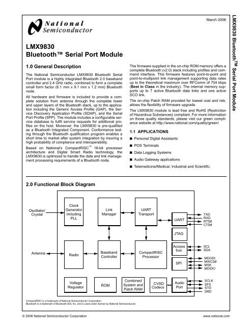
<strong>LMX9830</strong>Bluetooth <strong>Serial</strong> <strong>Port</strong> <strong>Module</strong>1.0 General DescriptionThe National Semiconductor <strong>LMX9830</strong> Bluetooth <strong>Serial</strong><strong>Port</strong> module is a highly integrated Bluetooth 2.0 basebandcontroller and 2.4 GHz radio, combined to form a completesmall form factor (6.1 mm x 9.1 mm x 1.2 mm) Bluetoothnode.All hardware and firmware is included to provide a completesolution from antenna through the complete lowerand upper layers of the Bluetooth stack, up to the applicationincluding the Generic Access Profile (GAP), the ServiceDiscovery Application Profile (SDAP), and the <strong>Serial</strong><strong>Port</strong> Profile (SPP). The module includes a configurable servicedatabase to fulfil service requests for additional profileson the host. Moreover, the <strong>LMX9830</strong> is pre-qualifiedas a Bluetooth Integrated Component. Conformance testingthrough the Bluetooth qualification program enables ashort time to market after system integration by insuring ahigh probability of compliance and interoperability.Based on National’s CompactRISC 16-bit processorarchitecture and Digital Smart Radio technology, the<strong>LMX9830</strong> is optimized to handle the data and link managementprocessing requirements of a Bluetooth node.The firmware supplied in the on-chip ROM memory offers acomplete Bluetooth (v2.0) stack including profiles and commandinterface. This firmware features point-to-point andpoint-to-multipoint link management supporting data ratesup to the theoretical maximum over RFComm of 704 kbps(Best in Class in the industry). The internal memory supportsup to 7 active Bluetooth data links and one activeSCO link.The on-chip Patch RAM provided for lowest cost and risk,allows the flexibility of firmware upgrade.The <strong>LMX9830</strong> module is lead free and RoHS (Restrictionof Hazardous Substances) compliant. For more informationon those quality standards, please visit our green compliancewebsite at http://www.national.com/quality/green/1.1 APPLICATIONS■ Personal Digital Assistants■ POS Terminals■ Data Logging Systems■ Audio Gateway applications■ Telemedicine/Medical, Industrial and Scientific.March 2006<strong>LMX9830</strong> Bluetooth TM <strong>Serial</strong> <strong>Port</strong> <strong>Module</strong>2.0 Functional Block DiagramOscillator/CrystalClockGeneratorincludingPLLLinkManagerUARTTransportUARTTXDRXDRTS#CTS#JTAGAntennaRadioBasebandControllerCompactRISCProcessorAccessbusSPISCLSDAMDODIMWCS#MSKMDIDOVoltageRegulatorROMCombinedSystem andPatch RAMCVSDCodecsAudio<strong>Port</strong>SCLKSFSSTDSRDCompactRISC is a trademark of National Semiconductor Corporation.Bluetooth is a trademark of Bluetooth SIG, Inc. and is used under license by National Semiconductor.© 2006 National Semiconductor Corporation www.national.com
<strong>LMX9830</strong>1.0 General Description . . . . . . . . . . . . . . . . . . . . . . . . . . . . 11.1 APPLICATIONS . . . . . . . . . . . . . . . . . . . . . . . . . . . 12.0 Functional Block Diagram . . . . . . . . . . . . . . . . . . . . . . . 13.0 Features . . . . . . . . . . . . . . . . . . . . . . . . . . . . . . . . . . . . . . 33.1 DIGITAL HARDWARE . . . . . . . . . . . . . . . . . . . . . . 33.2 FIRMWARE . . . . . . . . . . . . . . . . . . . . . . . . . . . . . . 33.3 DIGITAL SMART RADIO . . . . . . . . . . . . . . . . . . . . 33.4 PHYSICAL . . . . . . . . . . . . . . . . . . . . . . . . . . . . . . . 34.0 Order Information . . . . . . . . . . . . . . . . . . . . . . . . . . . . . . 35.0 Connection Diagram . . . . . . . . . . . . . . . . . . . . . . . . . . . . 46.0 Pad Description . . . . . . . . . . . . . . . . . . . . . . . . . . . . . . . 47.0 General Specifications . . . . . . . . . . . . . . . . . . . . . . . . . . 77.1 DC CHARACTERISTICS . . . . . . . . . . . . . . . . . . . 87.2 RF PERFORMANCE CHARACTERISTICS . . . . . 97.3 PERFORMANCE DATA (TYPICAL) . . . . . . . . . . 118.0 Functional Description . . . . . . . . . . . . . . . . . . . . . . . . . 138.1 BASEBAND AND LINK MANAGEMENTPROCESSORS . . . . . . . . . . . . . . . . . . . . . . . . . . 138.1.1 Bluetooth Lower Link Controller . . . . . . . . . . . . 138.1.2 Bluetooth Upper Layer Stack . . . . . . . . . . . . . . 138.1.3 Profile support . . . . . . . . . . . . . . . . . . . . . . . . . 138.1.4 Application with command interface . . . . . . . . . 138.1.5 Memory . . . . . . . . . . . . . . . . . . . . . . . . . . . . . . 138.1.6 External memory interfaces . . . . . . . . . . . . . . . 138.1.7 µ-wire/SPI interface . . . . . . . . . . . . . . . . . . . . . 138.1.8 Access.bus interface . . . . . . . . . . . . . . . . . . . . 148.2 TRANSPORT PORT - UART . . . . . . . . . . . . . . . . 148.3 AUDIO PORT . . . . . . . . . . . . . . . . . . . . . . . . . . . . 148.3.1 Advanced Audio Interface . . . . . . . . . . . . . . . . 148.4 AUXILIARY PORTS . . . . . . . . . . . . . . . . . . . . . . . 158.4.1 RESET# . . . . . . . . . . . . . . . . . . . . . . . . . . . . . . 158.4.2 General Purpose I/Os . . . . . . . . . . . . . . . . . . . 158.5 SYSTEM POWER UP . . . . . . . . . . . . . . . . . . . . . 158.6 STARTUP SEQUENCE . . . . . . . . . . . . . . . . . . . . 178.6.1 Options Register . . . . . . . . . . . . . . . . . . . . . . . 178.6.2 Startup With External PROM Available . . . . . . 178.6.3 Startup Without External PROM Available . . . . 178.6.4 Configuring the <strong>LMX9830</strong> throughtransport layer . . . . . . . . . . . . . . . . . . . . . . . . . 198.6.5 Auto Baud Rate Detection . . . . . . . . . . . . . . . . 198.7 USING AN EXTERNAL EEPROM FORNON-VOLATILE DATA . . . . . . . . . . . . . . . . . . . . 209.0 Digital Smart Radio . . . . . . . . . . . . . . . . . . . . . . . . . . . . 209.1 FUNCTIONAL DESCRIPTION . . . . . . . . . . . . . . 209.2 RECEIVER FRONT-END . . . . . . . . . . . . . . . . . . 209.2.1 Poly-Phase Bandpass Filter . . . . . . . . . . . . . . . 209.2.2 Hard-Limiter and RSSI . . . . . . . . . . . . . . . . . . . 209.3 RECEIVER BACK-END . . . . . . . . . . . . . . . . . . . . 209.3.1 Frequency Discriminator . . . . . . . . . . . . . . . . . 209.3.2 Post-Detection Filter and Equalizer . . . . . . . . . 209.4 AUTOTUNING CIRCUITRY . . . . . . . . . . . . . . . . . 219.5 SYNTHESIZER . . . . . . . . . . . . . . . . . . . . . . . . . . 219.5.1 Phase-Frequency Detector . . . . . . . . . . . . . . . 219.6 TRANSMITTER CIRCUITRY . . . . . . . . . . . . . . . . 219.6.1 IQ-DA Converters and TX Mixers . . . . . . . . . . 21Table of Contents9.7 CRYSTAL REQUIREMENTS . . . . . . . . . . . . . . . 219.7.1 Crystal . . . . . . . . . . . . . . . . . . . . . . . . . . . . . . . 219.7.2 TCXO (Temperature CompensatedCrystal Oscillator) . . . . . . . . . . . . . . . . . . . . . . 249.7.3 Optional 32 kHz Oscillator . . . . . . . . . . . . . . . 249.7.4 ESR (Equivalent Series Resistance) . . . . . . . 249.8 ANTENNA MATCHING AND FRONT-ENDFILTERING . . . . . . . . . . . . . . . . . . . . . . . . . . . . . 259.9 LOOP FILTER DESIGN . . . . . . . . . . . . . . . . . . . 259.9.1 Component Calculations . . . . . . . . . . . . . . . . . 259.9.2 Phase Noise and Lock-Time Calculations . . . 279.9.3 Practical Optimization . . . . . . . . . . . . . . . . . . . 289.9.4 Component Values for NSC ReferenceDesigns . . . . . . . . . . . . . . . . . . . . . . . . . . . . . . 3010.0 Integrated Firmware . . . . . . . . . . . . . . . . . . . . . . . . . . 3010.1 FEATURES . . . . . . . . . . . . . . . . . . . . . . . . . . . . 3010.1.1 Operation Modes . . . . . . . . . . . . . . . . . . . . . . 3010.1.2 Default Connections . . . . . . . . . . . . . . . . . . . . 3010.1.3 Event Filter . . . . . . . . . . . . . . . . . . . . . . . . . . . 3010.1.4 Default Link Policy . . . . . . . . . . . . . . . . . . . . . 3110.1.5 Audio Support . . . . . . . . . . . . . . . . . . . . . . . . . 3111.0 Low Power Modes . . . . . . . . . . . . . . . . . . . . . . . . . . . . 3211.1 POWER MODES . . . . . . . . . . . . . . . . . . . . . . . . 3211.2 ENABLING AND DISABLING UARTTRANSPORT 3211.2.1 Hardware Wake up functionality . . . . . . . . . . . 3211.2.2 Disabling the UART transport layer . . . . . . . . 3311.2.3 <strong>LMX9830</strong> enabling the UART interface . . . . . 3311.2.4 Enabling the UART transport layer fromthe host . . . . . . . . . . . . . . . . . . . . . . . . . . . . . . 3312.0 Command Interface . . . . . . . . . . . . . . . . . . . . . . . . . . . 3412.1 FRAMING . . . . . . . . . . . . . . . . . . . . . . . . . . . . . . 3412.1.1 Start and End Delimiter . . . . . . . . . . . . . . . . . . 3412.1.2 Packet Type ID . . . . . . . . . . . . . . . . . . . . . . . . 3412.1.3 Opcode . . . . . . . . . . . . . . . . . . . . . . . . . . . . . . 3412.1.4 Data Length . . . . . . . . . . . . . . . . . . . . . . . . . . 3412.1.5 Checksum: . . . . . . . . . . . . . . . . . . . . . . . . . . . 3412.2 COMMAND SET OVERVIEW . . . . . . . . . . . . . . 3513.0 Usage Scenarios . . . . . . . . . . . . . . . . . . . . . . . . . . . . . 3913.1 SCENARIO 1: POINT-TO-POINTCONNECTION . . . . . . . . . . . . . . . . . . . . . . . . . . 3913.2 SCENARIO 2: AUTOMATIC POINT-TO-POINTCONNECTION . . . . . . . . . . . . . . . . . . . . . . . . . . 4013.3 SCENARIO 3: POINT-TO-MULTIPOINT CONNEC-TION . . . . . . . . . . . . . . . . . . . . . . . . . . . . . . . . . . 4114.0 Reference design . . . . . . . . . . . . . . . . . . . . . . . . . . . . 4215.0 Soldering . . . . . . . . . . . . . . . . . . . . . . . . . . . . . . . . . . . 4316.0 Datasheet Revision History . . . . . . . . . . . . . . . . . . . . 4517.0 Physical Dimensions . . . . . . . . . . . . . . . . . . . . . . . . . . 46www.national.com 2
3.0 Features■ Compliant with the Bluetooth 2.0 Core Specification■ Better than -80 dBm input sensitivity■ Class 2 operation■ Low power consumption:■ High integration:– Implemented in 0.18 µm CMOS technology– RF includes antenna filter and switch on-chip3.1 DIGITAL HARDWARE■ Baseband and Link Management processors■ CompactRISC Core■ Embedded ROM and Patch RAM memory■ UART Command/Data <strong>Port</strong>:– Support for up to 921.6k baud rate■ Auxiliary Host Interface <strong>Port</strong>s:– Link Status– Transceiver Status (Tx or Rx)– Three General Purpose I/Os, available through theAPI– Alternative IO functions:– Link Status– Transport layer activity■ Advanced Power Management (APM) features– Advanced power management functions■ Advanced Audio Interface for external PCM codec■ ACCESS.bus and SPI/Microwire for interfacing with externalnon-volatile memory3.2 FIRMWARE■ Complete Bluetooth Stack including:– Baseband and Link Manager– L2CAP, RFCOMM, SDP– Profiles:– GAP– SDAP– SPP■ Additional Profile support on Host. e.g:– Dial Up Networking (DUN)– Facsimile Profile (FAX)– File Transfer Protocol (FTP)– Object Push Profile (OPP)– Synchronization Profile (SYNC)– Headset (HSP)– Handsfree Profile (HFP)– Basic Imaging Profile (BIP)– Basic Printing Profile (BPP)■ On-chip application including:– Default connections– Command Interface:– Link setup and configuration (also Multipoint)– Configuration of the module– Service database modifications– UART Transparent mode– Optimized cable replacement– Automatic transparent mode– Event filter3.3 DIGITAL SMART RADIO■ Accepts external clock or crystal input:– 13 MHz Typical– Supports 10 - 20 MHz– Secondary 32.768 kHz oscillator for low-powermodes– 20 ppm cumulative clock error required for Bluetooth■ Synthesizer:– Integrated VCO– Provides all clocking for radio and baseband functions■ Antenna <strong>Port</strong> (50 Ohms nominal impedance):– Embedded front-end filter for enhanced out of bandperformance■ Integrated transmit/receive switch (full duplex operationvia antenna port)■ Better than -80 dBm input sensitivity■ 0 dBm typical output power3.4 PHYSICAL■ Compact size - 6.1 mm x 9.1 mm x 1.2 mm■ Complete system interface provided in Ball Grid Array onunderside for surface mount assembly4.0 Order InformationTable 1. Order InformationOrder Number Spec Shipment Method<strong>LMX9830</strong>SM NOPB 1 388 pcs Tray<strong>LMX9830</strong>SMX NOPB 11. NOPB = No Pb (No Lead)2500 pcs Tape & Reel<strong>LMX9830</strong>3 www.national.com
<strong>LMX9830</strong>5.0 Connection Diagram1 2 3 4 5 6 7 8 9 10ABCDEFNC NC NC RDY# TMS XOSCEN PG6 VDD_IF TE VDD_RFRTS# GND RXD TCK TDI B_RESET_RA# RESET_BB# RESET_RA# GND_RF TST1/DIV2#OP6/SCL/MSK CTS# TXD VCC_IO VCC_CORE ENV1# TST2 TST3 TST4 GND_RFMDODI PG7 OP3/MWCS# OP7/SDA/MDIDO TDO OP4/PG4 GND_IF TST5 TST6 ANTVCC GND STD VCC_IOP X2_CKO VDD_IOR X1_CKI VDD_X1 GND_VCO GND_RFSCLK SFS SRD OP5 X2_CKI VCC_PLL X1_CKO VCO_OUT VCO_IN VDD_VCOX-ray - Top ViewFigure 1. Connection Diagram6.0 Pad DescriptionPad NamePadLocationTable 2. Pin DescriptionType Default Layout DescriptionX1_CKO F7 O Crystal 10-20 MHzX1_CKI E7 I Crystal or External Clock 10-20 MHzX2_CKI F5 I GND (if not 32.768 kHz Crystal Oscillator.used)X2_CKO E5 O NC (if not used) 32.768 kHz Crystal Oscillator.RESET_RA# B8 I Radio Reset (active low)B_RESET_RA# B6 O NC Buffered Reset Radio Output (active low)RESET_BB# B7 I Baseband Reset (active low)ENV1# C6 I NC ENV1: Environment Select (active low) used formanufacturing test onlyTE A9 I GND Test Enable - Used for manufacturing test onlyTST1/DIV2# B10 I NC TST1: Test Mode. Leave not connected to permit usewith VTune automatic tuning algorithmDIV2#: No longer supportedTST2 C7 I GND Test Mode, Connect to GNDTST3 C8 I GND Test Mode, Connect to GNDTST4 C9 I GND Test Mode, Connect to GNDTST5 D8 I GND Test Mode, Connect to GNDTST6 D9 I VCO_OUT Test Input,Connect to VCO_OUT via 0Ohm resistor to permituse with VTune automatic tuning algorithmwww.national.com 4
6.0 Pad Description (Continued)Pad NamePadLocationTable 2. Pin DescriptionType Default Layout Description<strong>LMX9830</strong>MDODI 1 D1 I/O SPI Master Out Slave InOP6/SCL/MSK C1 OP6: I See Table 17 onpage 17OP7/SDA/MDIDOD4SCL/MSK: I/OOP7: ISDA/MDIDO: I/OSee Table 17 onpage 17OP3/MWCS# D3 I See Table 17 onpage 17 andTable 18 on page19OP4/PG4 D6 OP4: IPG4: I/OSee Table 17 onpage 17 andTable 18 on page19OP5 F4 I/O See Table 17 onpage 17 andTable 18 on page19OP6: Pin checked during Startup Sequence for configurationoptionSCL: ACCESS.Bus ClockMSK: SPI ShiftOP7: Pin checked during Startup Sequence for configurationoptionSDA: ACCESS.Bus <strong>Serial</strong> DataMDIDO: SPI Master In Slave OutOP3: Pin checked during Startup Sequence for configurationoptionMWCS#: SPI Slave Select Input (active low)OP4: Pin checked during Startup Sequence for configurationoptionPG4: GPIOOP5: Pin checked during Startup Sequence for configurationoptionSCLK F1 I/O Audio PCM Interface ClockSFS F2 I/O Audio PCM Interface Frame SynchronizationSRD F3 I Audio PCM Interface Receive Data InputSTD E3 O Audio PCM Interface Transmit Data OutputXOSCEN A6 O Clock Request. Toggles with X2 (LP0) crystalenable/disablePG6 A7 I/O GPIOPG7 D2 I/O GPIO - Default setup RF traffic LED indicationCTS# 2 C2 I GND (if not Host <strong>Serial</strong> <strong>Port</strong> Clear To Send (active low)used)RXD B3 I Host <strong>Serial</strong> <strong>Port</strong> Receive DataRTS# 3 B1 O NC (if not used) Host <strong>Serial</strong> <strong>Port</strong> Request To Send (active low)TXD C3 O Host <strong>Serial</strong> <strong>Port</strong> Transmit DataRDY# A4 O NC JTAG Ready Output (active low)TCK B4 I NC JTAG Test Clock InputTDI B5 I NC JTAG Test Data InputTDO D5 O NC JTAG Test Data OutputTMS A5 I NC JTAG Test Mode Select InputVCO_OUT F8 O Charge Pump Output, connect to Loop filterVCO_IN F9 I VCO Tuning Input, feedback from Loop filterANT D10 I/O RF Antenna 50 ohm Nominal ImpedanceVCC_PLL F6 O 1.8V Core Logic Power Supply OutputVCC_CORE C5 O 1.8V Voltage Regulator Output5 www.national.com
<strong>LMX9830</strong>6.0 Pad Description (Continued)Pad NamePadLocationTable 2. Pin DescriptionType Default Layout DescriptionVDD_X1 E8 I Power Supply Crystal OscillatorVDD_VCO F10 I Power Supply VCOVDD_RF A10 I Power Supply RFVDD_IOR E6 I Power Supply I/O Radio/BBVDD_IF A8 I Power Supply IFVCC_IOP E4 I Power Supply Audio InterfaceVCC_IO C4 I Power Supply I/OVCC E1 I Voltage Regulator InputGND_VCO E9 GroundGND_RF B9, C10,GroundE10GND_IF D7 GroundGND B2,E2 GroundNC A1,A2,A3 NC Treat as no connect. Place pad for mechanical stability1. Must use 1k ohm pull up2. Connect to GND if CTS is not use.3. Treat as No Connect if RTS is not used. Pad required for mechanical stability.www.national.com 6
7.0 General SpecificationsAbsolute Maximum Ratings (see Table 3) indicate limitsbeyond which damage to the device may occur. OperatingRatings (see Table 4) indicate conditions for which thedevice is intended to be functional.This device is a high performance RF integrated circuit andis ESD sensitive. Handling and assembly of this deviceshould be performed at ESD free workstations.The following conditions are true unless otherwise stated inthe tables below:■ T A = -40°C to +85°C■ VCC = 3.3V■ RF system performance specifications are guaranteedon National Semiconductor Mesa board rev 1.1 referencedesign platform.<strong>LMX9830</strong>Table 3. Absolute Maximum RatingsSymbol Parameter Min Max UnitVCC Digital Voltage Regulator input -0.2 4.0 VV I Voltage on any pad with GND = 0V -0.2 VCC + 0.2 VVDD_RF Supply Voltage Radio 0.2 3.3 VVDD_IFVDD_X1VDD_VCOP IN RF RF Input Power 0 dBmV ANT Applied Voltage to ANT pad 1.95 VT S Storage Temperature Range -65 +150 o CT L Lead Temperature 1 (solder 4 sec.) 225 o CT LNOPB Lead Temperature NOPB 1,2 (solder 40 sec.) 260 °CESD HBM ESD - Human Body Model 2000 VESD MM ESD - Machine Model 200 3 V1. Reference IPC/JDEC J-STD-20C spec.2. NOPB = No Pb (No Lead)3. A 200V ESD rating applies to all pins except OP3, OP6, OP7, MDODI, SCLK, SFS, STD, TDO, and ANT pins = 150V.Table 4. Recommended Operating ConditionsSymbol Parameter Min Typ Max UnitVCC Digital Voltage Regulator input 2.5 2.75 3.6 VT R Digital Voltage Regulator Rise Time 10 usT AAmbient Operating Temperature Range-40 +25 +125Fully Functional Bluetooth Nodeo CVCC_IO Supply Voltage Digital I/O 1.6 3.3 3.6 VVCC_PLLInternally connected to VCC_CoreVDD_RF Supply Voltage Radio 2.5 2.75 3.0 VVDD_IFVDD_X1VDD_VCOVDD_IOR Supply Voltage Radio I/O 1.6 2.75 VDD_RF VVCC_IOP Supply Voltage PCM Interface 1.6 3.3 3.6 VVCC_CORE Supply Voltage Output 1.8 VVCC_CORE MAX Supply Voltage Output Max Load 5 mAVCC_CORE SHORT When used as Supply Input (VCC grounded) 1.6 1.8 2.0 V7 www.national.com
<strong>LMX9830</strong>7.0 General Specifications (Continued)Table 5. Power Supply Requirements 1,2Symbol Parameter Min Typ 3 Max UnitI CC-TX Power supply current for continuous transmit 65 mAI CC-RX Power supply current for continuous receive 65 mAI RXSL Receive Data in SPP Link, Slave4 26 mAI RXM Receive Data in SPP Link, Master4 23 mAI SnM Sniff Mode, Sniff interval 1 second4 5.6 mAI SC-TLDIS Scanning, No Active Link, TL Disabled 4 0.43 mAI Idle Idle, Scanning Disabled, TL Disabled 4 100 µA1. Power supply requirements based on Class II output power.2. Based on UART Baudrate 921.6kbit/s.3. VCC = 3.3V, VCC_IO = 3.3V, Ambient Temperature = +25 °C.4. Average values excluding IO7.1 DC CHARACTERISTICSTable 6. Digital DC CharacteristicsSymbol Parameter Condition Min Max UnitsV IH Logical 1 Input Voltage high 1.6V ≤ VCC_IO ≤ 3.0V 0.7 x VCC_IO VCC_IO + 0.2 V(except oscillator I/O)3.0V ≤ VCC_IO ≤ 3.6V 2.0 VCC_IO + 0.2V IL Logical 0 Input Voltage low 1.6V ≤ VCC_IO ≤ 3.0V -0.2 0.25 x VCC_IO V(except oscillator I/O)3.0V ≤ VCC_IO ≤ 3.6V -0.20.8V HYS Hysteresis Loop Width 1 0.1 x VCC_IO VI OH Logical 1 Output Current V OH = 2.4V,VCC_IO = 3.0VI OL Logical 0 Output Current V OH = 0.4V,VCC_IO = 3.0V1. Guaranteed by design.-10 mA10 mAwww.national.com 8
7.0 General Specifications (Continued)7.2 RF PERFORMANCE CHARACTERISTICSIn the performance characteristics tables the followingapplies:■ All tests performed are based on Bluetooth Test Specificationrevision 2.0.■ All tests are measured at antenna port unless otherwisespecified■ T A = -40°C to +85°CTable 7. Receiver Performance Characteristics■ VDD_RF = 2.8V unless otherwise specifiedRF system performance specifications are guaranteed onNational Semiconductor Mesa Board rev 1.1 reference designplatform.<strong>LMX9830</strong>Symbol Parameter Condition Min Typ 1 Max UnitRX sense Receive Sensitivity BER < 0.001 2.402 GHz -80 -76 dBm2.441 GHz -80 -76 dBm2.480 GHz -80 -76 dBmPinRF Maximum Input Level -10 0 dBmIMP 2,3 Intermodulation Performance F 1 = + 3 MHz,-38 -36 dBmF 2 = + 6 MHz,P in RF = -64 dBmRSSI RSSI Dynamic Range at LNA Input -72 -52 dBm3Z Input Impedance of RF <strong>Port</strong> Single input impedance32 ΩRFIN(RF_inout)F in = 2.5 GHzReturn Loss 3 Return Loss -8 dBOOB 2,3 Out Of Band BlockingPerformanceP in RF = -10 dBm,30 MHz < F CWI < 2 GHz,BER < 0.001-10 dBmP in RF = -27 dBm,2000 MHz < F CWI < 2399 MHz,BER < 0.001P in RF = -27 dBm,2498 MHz < F CWI < 3000 MHz,BER < 0.001P in RF = -10 dBm,3000 MHz < F CWI < 12.75 GHz,BER < 0.001-27 dBm-27 dBm-10 dBm1. Typical operating conditions are at 2.75V operating voltage and 25 o C ambient temperature.2. The f 0 = -64 dBm Bluetooth modulated signal, f 1 = -39dbm sine wave, f 2 = -39 dBm Bluetooth modulated signal, f 0 = 2f 1- f 2 , and |f 2 - f 1 | = n * 1MHz, where n is 3, 4, or 5. For the typical case, n = 3.3. Not tested in production9 www.national.com
<strong>LMX9830</strong>7.0 General Specifications (Continued)Table 8. Transmitter Performance CharacteristicsSymbol Parameter Condition Min Typ 1 Max UnitP OUT RF Transmit Output Power 2.402 GHz -4 0 +3 dBm2.441 GHz -4 0 +3 dBm2.480 GHz -4 0 +3 dBmMOD ∆F1 AVG Modulation Characteristics Data = 00001111 140 165 175 kHzMOD ∆F2 MAX 2 Modulation Characteristics Data = 10101010 115 125 kHz∆F2 3AVG /∆F1 AVGModulation Characteristics 0.820 dB Bandwidth 1000 kHzP OUT 2*f o4PA 2 nd HarmonicSuppressionMaximum gain setting:f 0 = 2402 MHz,P out = 4804 MHz-30 dBmZ RFOUT5RF Output Impedance/InputImpedance of RF <strong>Port</strong>(RF_inout)P out @ 2.5 GHz 47 Ω1. Typical operating conditions are at 2.75V operating voltage and 25 o C ambient temperature.2. ∆F2max > 115 kHz for at least 99.9% of all ∆f2max.3. Modulation index set between 0.28 and 0.35.4. Out-of-Band spurs only exist at 2nd and 3rd harmonics of the CW frequency for each channel.5. Not tested in production.Table 9. Synthesizer Performance CharacteristicsSymbol Parameter Condition Min Typ Max Unitf VCO VCO Frequency Range 2402 2480 MHzt LOCK Lock Time f 0 + 20 kHz 120 µs∆f 0 offset 1 Initial Carrier Frequency Tolerance During preamble -75 0 75 kHz∆f 0 drift 1 Initial Carrier Frequency Drift DH1 data packet -25 0 25 kHzDH3 data packet -40 0 40 kHzDH5 data packet -40 0 40 kHzDrift Rate -20 0 20 kHz/50µst D -Tx Transmitter Delay Time From Tx data to antenna 4 µs1. Frequency accuracy is dependent on crystal oscillator chosen. The crystal must have a cumulative accuracy of < +/-20ppm to meet Bluetooth specifications.www.national.com 10
7.0 General Specifications (Continued)7.3 PERFORMANCE DATA (TYPICAL)<strong>LMX9830</strong>Figure 2. ModulationFigure 4. Corresponding Eye DiagramFigure 5. Synthesizer Phase NoiseFigure 3. Transmit SpectrumFilter Insertion Loss0-2-4IL (dB)-6-8-102.1E+09 2.2E+09 2.3E+09 2.4E+09 2.5E+09 2.6E+09 2.7E+09 2.8E+09Frequency (Hz)Figure 6. Front-End Bandpass Filter Response11 www.national.com
<strong>LMX9830</strong>7.0 General Specifications (Continued)1.002.000.50S(1.1)0.000.50m11.00m22.00m2freq=2.402ghzS(1.1)=0.093/-29.733impedance = Z0* (1.170 - j0.109)-2.00m1freq=2.500ghzS(1.1)=0.035/175.614impedance = Z0* (0.933 + j0.005)-1.00freq(2.400ghz to 2.500ghz)Figure 7. TX and RX Pin 50Ω Impedance Characteristics0.0-0.6-1.6-2.6-3.6-4.6db(s(1.1))-5.6-6.6-7.6-8.6m4m4freq=2.402GHzdB(S(1.1))=-8.282m3freq=2.441GHzdB(S(1.1))=-9.313m3m5freq=2.483GHzdB(S(1.1))=-9.227m5-9.62.5002.4952.4852.4802.4752.4702.4652.4602.4552.4502.4452.4402.4352.4302.4252.4202.4152.4102.400freq. ghzFigure 8. Transceiver Return Losswww.national.com 12
8.0 Functional Description8.1 BASEBAND AND LINK MANAGEMENTPROCESSORSBaseband and Lower Link control functions are implementedusing a combination of National Semiconductor’sCompactRISC 16-bit processor and the Bluetooth LowerLink Controller. These processors operate from integratedROM memory and RAM and execute on-board firmwareimplementing all Bluetooth functions.8.1.1 Bluetooth Lower Link ControllerThe integrated Bluetooth Lower Link Controller (LLC) complieswith the Bluetooth Specification version 2.0 andimplements the following functions:■ Adaptive Frequency Hopping■ Interlaced Scanning■ Fast Connect■ Support for 1, 3, and 5 slot packet types■ 79 Channel hop frequency generation circuitry■ Fast frequency hopping at 1600 hops per second■ Power management control■ Access code correlation and slot timing recovery8.1.2 Bluetooth Upper Layer StackThe integrated upper layer stack is prequalified andincludes the following protocol layers:■ L2CAP■ RFComm■ SDP8.1.3 Profile supportThe on-chip application of the <strong>LMX9830</strong> allows full standaloneoperation, without any Bluetooth protocol layer necessaryoutside the module. It supports the Generic AccessProfile (GAP), the Service Discovery Application Profile(SDAP), and the <strong>Serial</strong> <strong>Port</strong> Profile (SPP).The on-chip profiles can be used as interfaces to additionalprofiles executed on the host. The <strong>LMX9830</strong> includes aconfigurable service database to answer requests with theprofiles supported.8.1.4 Application with command interfaceThe module supports automatic slave operation eliminatingthe need for an external control unit. The implementedtransparent option enables the chip to handle incomingdata raw, without the need for packaging in a special format.The device uses a pin to block unallowed connections.This pincode can be fixed or dynamically set.Acting as master, the application offers a simple but versatilecommand interface for standard Bluetooth operationlike inquiry, service discovery, or serial port connection.The firmware supports up to seven slaves. Default Link Policysettings and a specific master mode allow optimizedconfiguration for the application specific requirements. Seealso Section "Integrated Firmware" on page 30.8.1.5 MemoryThe <strong>LMX9830</strong> introduces 16 kB of combined system andPatch RAM memory that can be used for data and/or codeupgrades of the ROM based firmware. Due to the flexiblestartup used for the <strong>LMX9830</strong> operating parameters likethe Bluetooth Device Address (BD_ADDR) are defined duringboot time. This allows reading out the parameters of anexternal EEPROM or programming them directly overUART.8.1.6 External memory interfacesAs the <strong>LMX9830</strong> is a ROM based device with no on-chipnon volatile storage, the operation parameters will be lostafter a power cycle or hardware reset. In order to prevent reinitializing such parameters, patches or even user data, the<strong>LMX9830</strong> offers two interfaces to connect an externalEEPROM to the device:■ µ-wire/SPI■ Access.bus (I 2 C compatible)The selection of the interface is done during start up basedon the option pins. See Table 17 on page 17 for the optionpin descriptions.8.1.7 µ-wire/SPI interfaceIn case the firmware is configured by the option pins to usea µ-wire/SPI EEPROM, the <strong>LMX9830</strong> will activate that interfaceand try to read out data from the EEPROM. The externalmemory needs to be compatible to the reference listedin Table 10 on page 13. The largest size EEPROM supportedis limited by the addressing format of the selected NVM.The device must have a page size equal to N x 32 bytes.The firmware requires that the EEPROM supports Pagewrite. Clock must be HIGH when idle.Table 10. M95640-S EEPROM 8Kx8ParameterValueSupplier ST MicroelectronicsSupply Voltage 1 1.8 - 3.6VSPI compatible (positive clock SPIInterface Modes)Memory Size 8K x 8, 64kbitClock Rate 1 2 MHzAccessByte and Page Write (up to32bytes)1. Parameter range reduced to requirements of Nationalreference design<strong>LMX9830</strong>13 www.national.com
<strong>LMX9830</strong>8.0 Functional Description (Continued)8.1.8 Access.bus interfaceIn case the firmware is configured by the option pins to usean access.bus or i 2 c compatible EEPROM, the <strong>LMX9830</strong>will activate that interface and try to read out data from theEEPROM. The external memory needs to be compatible tothe reference listed in Table 11 on page 14.The largest size EEPROM supported is limited by theaddressing format of the selected NVM. The device musthave a page size equal to N x 32 bytes.The device uses a 16 bit address format. The deviceaddress must be “000”.Table 11. 24C64 EEPROM 8kx8ParameterValueSupplierAtmelSupply Voltage 1 2.7 - 5.5 VInterface 2 wire serial interfaceMemory Size 8K x 8, 64kbitClock Rate 1 100 KHzAccess32 Byte Page Write Mode1. Parameter range reduced to requirements of Nationalreference design8.2 TRANSPORT PORT - UARTThe <strong>LMX9830</strong> provides one Universal AsynchronousReceiver Transmitter (UART). The UART interface consistsout of Receive (RX), Transmit (TX), Ready-to-Send (RTS)and Clear-to-Send signals. RTS and CTS are used forhardware handshaking between the host and the<strong>LMX9830</strong>. Since the <strong>LMX9830</strong> acts as gateway betweenthe bluetooth and the UART interface, National Semiconductorrecommends to use the handshaking signals especiallyfor transparent operation. In case two signals areused CTS needs to be pulled to GND. Please refer also to“<strong>LMX9830</strong> Software User’s Guide” for detailed informationon 2-wire operation.The UART interface supports formats of 8-bit data with orwithout parity, with one or two stop bits. It can operate atstandard baud rates from 2400bits/s up to a maximumbaud rate of 921.6kbits/s. DMA transfers are supported toallow for fast processor independent receive and transmitoperation.The UART baudrate is configured during startup by checkingoption pins OP3, OP4 and OP5 for reference clock andbaudrate. In case Auto baud rate detect is chosen, thefirmware check the NVS area if a valid UART baudrate hasbeen stored in a previous session. In case, no useful valuecan be found the device will switch to auto baud rate detectionand wait for an incoming reference signal.The UART offers wakeup from the power save modes viathe multi-input wakeup module. When the <strong>LMX9830</strong> is inlow power mode, RTS# and CTS# can function asHost_WakeUp and Bluetooth_WakeUp respectively. Table12 on page 14 represents the operational modes supportedby the firmware for implementing the transport viathe UART.Table 12. UART Operation ModesItem Range Default at Power-Up With Auto-DetectBaud Rate 2.4 to 921.6 kbits/s Either configured by option pins, NVS 2.4 to 921.6 kbits/sparameter or auto baud rate detectionFlow Control RTS#/CTS# or None RTS#/CTS# RTS#/CTS#Parity Odd, Even, None None NoneStop Bits 1,2 1 1Data Bits 8 8 88.3 AUDIO PORT8.3.1 Advanced Audio InterfaceThe Advanced Audio Interface (AAI) is an advanced versionof the Synchronous <strong>Serial</strong> Interface (SSI) that providesa full-duplex communications port to a variety ofindustry-standard 13/14/15/16-bit linear or 8-bit log PCMcodecs, DSPs, and other serial audio devices.The interface allows the support one codec or interface.The firmware selects the desired audio path and interfaceconfiguration by a parameter that is located in RAM(imported from non-volatile storage or programmed duringboot-up). The audio path options include the MotorolaMC145483 codec, the OKI MSM7717 codec, the WinbondW681360/W681310 codecs and the PCM slave throughthe AAI.In case an external codec or DSP is used the <strong>LMX9830</strong>audio interface generates the necessary bit and frameclock driving the interface.Table 13 on page 15 summarizes the audio path selectionand the configuration of the audio interface at the specificmodes.The <strong>LMX9830</strong> supports one SCO link.www.national.com 14
8.0 Functional Description (Continued).Table 13. Audio path configuration<strong>LMX9830</strong>Audio setting Interface Freq FormatAAI BitClockAAI FrameClockAAI Frame SyncPulse LengthOKIMSM7717Advanced audiointerfaceANY 18-bit log PCM(a-law only)480 KHz 8 KHz 14 BitsMotorolaMC145483 2Advanced audiointerface13-bit linear 480 KHz 8 KHz 13 BitsOKIMSM7717Advanced audiointerface13MHz8-bit log PCM(a-law only)520 KHz 8 KHz 14 BitsMotorolaMC145483 3Advanced audiointerface13-bit linear 520 KHz 8 KHz 13 BitsWinbondW681310Advanced audiointerface13MHz8 bit log PCMA-law and u-law520 KHz 8 KHz 14 BitsWinbondW681360Advanced audiointerface13MHz 13-bit linear 520 KHz 8 KHz 13 BitsPCM slave 4Advanced audiointerfaceANY 1 8/16 bits 128 - 1024KHz8 KHz 8/16 Bits1. For supported frequencies see Table 22 on page 242. Due to internal clock divider limitations the optimum of 512KHz, 8KHz can not be reached. The values are set to thebest possible values. The clock mismatch does not result in any discernible loss in audio quality.3. Due to internal clock divider limitations the optimum of 512KHz, 8KHz can not be reached. The values are set to thebest possible values. The clock mismatch does not result in any discernible loss in audio quality.4. In PCM slave mode, parameters are stored in NVS. Bit clock and frame clock must be generated by the host interface.PCM slave configuration example: PCM slave uses the slot 0, 1 slot per frame, 16 bit linear mode, long frame sync, normalframe sync. In this case, 0x03E0 should be stored in NVS. See “<strong>LMX9830</strong> Software User’s Guide” for more details.8.4 AUXILIARY PORTS8.4.1 RESET#There are two reset inputs: RESET_RA# for the radio andRESET_BB# for the baseband. Both are active low.There is also a reset output, B_RESET_RA# (BufferedRadio Reset) active low. This output follows inputRESET_RA#.When RESET_RA# is released, going high,B_RESET_RA# stays low until the clock has started.Please see Section 8.5 "System Power Up" on page 15 fordetails.8.4.2 General Purpose I/OsThe <strong>LMX9830</strong> offers 3 pins which either can be used asindication and configuration pins or can be used for GeneralPurpose functionality. The selection is made out of settingsderived out of the power up sequence.In General Purpose configuration the pins are controlledhardware specific commands giving the ability to set thedirection, set them to high or low or enable a weak pull-up.In alternate function the pins have pre-defined indicationfunctionality. Please see Table 14 on page 15 for a descriptionon the alternate indication functionality.Table 14. Alternate GPIO pin configurationPinOP4/PG4PG6PG7DescriptionOperation Mode pin to configure TransportLayer settings during boot-upGPIORF Traffic indication8.5 SYSTEM POWER UPIn order to correctly power-up the <strong>LMX9830</strong> the followingsequence is recommended to be performed:Apply VCC_IO and VCC to the <strong>LMX9830</strong>.The RESET_RA# should be driven high. ThenRESET_BB# should be driven high at a recommendedtime of 1ms after the <strong>LMX9830</strong> voltage rails are high. The<strong>LMX9830</strong> is properly reset.Please see timing diagram, Figure 9 on page 16.15 www.national.com
<strong>LMX9830</strong>8.0 Functional Description (Continued)ESR of the crystal also has impact on the startup time ofthe crystal oscillator circuit of the <strong>LMX9830</strong> (SeeTable 15and Table 16 on page 16).all VCC and VDD linest PTORRARESET_RA#t PTORBBRESET_BB#X1_CKO<strong>LMX9830</strong>Initialization<strong>LMX9830</strong>OscillatorStart-Up<strong>LMX9830</strong> inPower-Up Mode<strong>LMX9830</strong> in Normal ModeFigure 9. <strong>LMX9830</strong> Power on Reset TimingTable 15. <strong>LMX9830</strong> Power to Reset timingSymbol Parameter Condition Min Typ Max Unitt PTORRA Power to Reset _RA# V CC and VCC_IO at operatingvoltage level to valid resett PTORBB Reset_RA# to Reset_BB# V CC and VCC_IO at operatingvoltage level to valid reset1. Rise time on power must switch on fast, rise time
8.0 Functional Description (Continued)8.6 STARTUP SEQUENCEDuring startup the <strong>LMX9830</strong> checks the options registerpins OP3 to OP7 for configuration on operation mode, externalclock source, transport layer and available non volatilestorage PROM.The different options for startup are described in Table 17 onpage 17.8.6.1 Options RegisterExternal pads in Table 17 on page 17 are latched in this registerat the end of Reset. The Options register can be readby firmware at any time.All pads are inputs with weak on-chip pull-up/down resistorsduring Reset. Resistors are disconnected at the end ofRESET_BB#.1 = Pull-up resistor connected in application0 = Pull-down resistor connected in applicationx = Don’t care8.6.2 Startup With External PROM AvailableTo be able to read out information from an external PROMthe option pins have to be set according to Table 17 on page17.Startup sequence activities:1. From the Options registers OP6 and OP7, the <strong>LMX9830</strong>checks if a serial PROM is available to use (AC-CESS.bus or Microwire).2. If serial PROM is available, the permanent parameterblock, patch block, and non-volatile storage (NVS) areread from it. If the BD Address is not present, enter theBD address to be saved in the NVS. For more informationsee Section 8.6.4 "Configuring the <strong>LMX9830</strong>through transport layer" on page 193. From the Options register OP3, OP4 and OP5, the<strong>LMX9830</strong> checks for clocking information and transportlayer settings. If the NVS information are not sufficient,the <strong>LMX9830</strong> will send the “Await Initialization” event onthe TL (Transport Layer) and wait for additional information(see Section 8.6.3 "Startup Without External PROMAvailable" on page 17.)4. The <strong>LMX9830</strong> compensates the UART for new BBCLKinformation from the NVS.5. The <strong>LMX9830</strong> starts up the Bluetooth core.8.6.3 Startup Without External PROM AvailableThe following sequence will take place if OP6 and OP7 havebeen set to “No external memory” as described in Table 17on page 17.Startup sequence activities:1. From the Options registers OP6 and OP7, the <strong>LMX9830</strong>checks if a serial PROM is available to use.2. From the Options register OP3, OP4 and OP5, the<strong>LMX9830</strong> checks for clocking mode and transport layer.3. The <strong>LMX9830</strong> sends the “Await Initialization” Event onthe TL (Transport Layer) and waits for NVS configurationcommands. The configuration is finalized by sending the“Enter Bluetooth Mode” command.4. The <strong>LMX9830</strong> compensates the UART for new BBCLKinformation from the NVS.5. The <strong>LMX9830</strong> starts up the Bluetooth core.<strong>LMX9830</strong>Table 17. Startup Sequence Options 1Package PadCommentOP3 OP4 OP5 OP6 2 OP7 3 ENV1#PD PD PD PD PD PU PD = Internal Pull-down during ResetPU = Internal Pull-up during Resetx x x Open (0) Open (0) Open (1) No serial memoryBBCLKx x x 1 Open (0) Open (1) TBDBBCLKx x x Open (0) 1 Open (1) Microwire serial memoryBBCLKx x x 1 1 Open (1) ACCESS.bus serial memoryBBCLKT_SCLK x x T_RFDATAT_RFCE 0 BBCLK Test mode1. 1/0 pull-up/down resistor connected in application.2. If OP6 is 1, must use 1k ohm pull up3. If OP7 is 1, must use 1k ohm pull up17 www.national.com
<strong>LMX9830</strong>8.0 Functional Description (Continued)Power Up orResetInitialization ModeOP3/4/5Clock definition10-20MHzClock definedin EEPROMno12 or 13MHzyesOP3/4/5UART speedRead fromNVSUART speeddefined inEEPROMnoHost sends 0x01 for Autobaudrate,waiting for“Await Initialization Event”from <strong>LMX9830</strong>9.6/115.2/921.6yesHost sends “Set ClockAnd Baud Rate”BD_Addrdefined inEEPROMno<strong>LMX9830</strong> sends “AwaitInitialization Event” incase not already happened.yesHost sends “ChangeLocal Bluetooth Address”Optionally host sends other configurationparameters or patch using“WriteROM Patch”If <strong>LMX9830</strong> sent “Await InitializationEvent” , Host sends “Enter BluetoothMode”, otherwise done automatically<strong>LMX9830</strong>sends”<strong>LMX9830</strong> Ready”Bluetooth ModeFigure 10. Flow Diagram for the Start-up Sequencewww.national.com 18
8.0 Functional Description (Continued)Table 18. Fixed Frequencies<strong>LMX9830</strong>Osc Freq.(MHz)BBCLK(MHz)PLL(48 MHz)OP3 1 OP4 2 OP5 3 Function12 12 OFF 0 0 0 UART speed read from NVS10-20 4 10-20 1 ON 0 1 0 Clock and UART baudrate detection13 13 OFF 1 0 0 UART speed read from NVS13 13 OFF 1 0 1 UART speed 9.6 kbps13 13 OFF 1 1 0 UART speed 115.2 kbps13 13 OFF 1 1 1 UART speed 921.6 kbps1. If OP3 is 1, must use 1k ohm pull up.2. If OP4 is 1, must use 1k ohm pull up.3. If OP5 is 1, must use 1k ohm pull up.4. Supported frequencies see Table 22 on page 248.6.4 Configuring the <strong>LMX9830</strong> through transport layerAs described in Section 8.5 "System Power Up" on page 15,the <strong>LMX9830</strong> will check during startup the Options Registersif an external PROM is available. If the information onthe PROM are incomplete or no PROM is installed the<strong>LMX9830</strong> will boot into the “initialization Mode”.The mode is confirmed by the “Await Initialization” Event.The following information are needed to enter BluetoothMode:■ Bluetooth Device Address (BD_Addr)■ External clock source (only if 10 - 20 MHz has beenselected)■ UART Baudrate (only if Auto baudrate detection hasbeen selected)In general the following procedure will initialize the<strong>LMX9830</strong>:1. Wait for “Await initialization” Event- Event will only appear if transport layer speed is set orafter successful baudrate detection.2. Send “Set Clock and Baudrate” Command only if theclock speed is not known through hardware configuration(i.e only if OP3 OP4 OP5 = 0 1 0).3. Send “Write BD_Addr” to Configure Local Bluetooth DeviceAddress.4. Send “Enter Bluetooth Mode”- <strong>LMX9830</strong> will use configured clock and UART speedand start the command interface.NOTE: In case no EEPROM is used, BDAddr, clock sourceand Baudrate are only valid until the next power-cycle orhardware reset.8.6.5 Auto Baud Rate DetectionThe <strong>LMX9830</strong> supports an Automatic Baudrate Detection incase the external clock is different to 12, 13MHz or therange 10-20 MHz or the baudrate is different to 9.6 kbps,115.2 or 921.6kbit/s.The baudrate detection is based on the measurement of asingle character. The following issues need to be considered:■ The flow control pin CTS must be low or else the host isin flow stop.■ The Auto Baudrate Detector measures the length of the0x01 character from the positive edge of bit 0 to thepositive edge of stop bit.■ Therefore the very first received character must alwaysbe a 0x01.■ The host can restrict itself to send only a 0x01 characteror also can send a command.■ The host must flush the TX buffer within 50-100 millisecondsdepend on clock frequency on the host controller.■ After 50-100 milliseconds the UART is about to be initializedand short after the host should receive a “AwaitInitialization” Event or an “Command Status” Event.CTSRX0x01 0x00 50 - 100ms delayFigure 11. Auto baudrate detection timing diagram19 www.national.com
<strong>LMX9830</strong>9.0 Digital Smart Radio (Continued)8.7 USING AN EXTERNAL EEPROM FOR NON-VOLATILE DATAThe <strong>LMX9830</strong> offers two interfaces to connect to externalmemory. Depending on the EEPROM used, the interface isactivated by setting the correct option pins during start up.See Table 17 on page 17 for the option pin settings.The external memory is used to store mandatory parameterslike the BD_Address as well as many optional parameterslike Link Keys or even User data.The NVM is organized with fixed addresses for the parameters.Because of that the EEPROM can be preprogrammedwith default parameters in manufacturing. Refer to "OperationParameters Stored in <strong>LMX9830</strong>" for the organization ofthe NVS map.In case the external memory is empty on first startup the<strong>LMX9830</strong> will behave as like no memory is connected. (SeeSection 8.6.3 "Startup Without External PROM Available"on page 17). During the startup process parameters can bewritten directly to the EEPROM to be available after nextbootup. On first bootup, the EEPROM will be automaticallyprogrammed to default values, including the UART speed of9600 BPS. Patches supplied over the TL will be stored automaticallyinto the EEPROM.9.0 Digital Smart Radio9.1 FUNCTIONAL DESCRIPTIONThe integrated Digital Smart Radio utilizes a heterodyne receiverarchitecture with a low intermediate frequency (2MHz) such that the intermediate frequency filters can be integratedon chip. The receiver consists of a low-noise amplifier(LNA) followed by two mixers. The intermediatefrequency signal processing blocks consist of a poly-phasebandpass filter (BPF), two hard-limiters (LIM), a frequencydiscriminator (DET), and a post-detection filter (PDF). Thereceived signal level is detected by a received signalstrength indicator (RSSI).The received frequency equals the local oscillator frequency(fLO) plus the intermediate frequency (fIF):fRF = fLO + fIF (supradyne).The radio includes a synthesizer consisting of a phase detector,a charge pump, an (off-chip) loop-filter, an RF-frequencydivider, and a voltage controlled oscillator (VCO).The transmitter utilizes IQ-modulation with bit-stream datathat is gaussian filtered. Other blocks included in the transmitterare a VCO buffer and a power amplifier (PA).9.2 RECEIVER FRONT-ENDThe receiver front-end consists of a low-noise amplifier(LNA) followed by two mixers and two low-pass filters for theI- and Q-channels.The intermediate frequency (IF) part of the receiver frontendconsists of two IF amplifiers that receive input signalsfrom the mixers, delivering balanced I- and Q-signals to thepoly-phase bandpass filter. The poly-phase bandpass filteris directly followed by two hard-limiters that together generatean AD-converted RSSI signal.9.2.1 Poly-Phase Bandpass FilterThe purpose of the IF bandpass filter is to reject noise andspurious (mainly adjacent channel) interference that wouldotherwise enter the hard limiting stage. In addition, it takescare of the image rejection.The bandpass filter uses both the I- and Q-signals from themixers. The out-of-band suppression should be higher than40 dB (f3 MHz). The bandpass filter is tuned overprocess spread and temperature variations by the autotunercircuitry. A 5th order Butterworth filter is used.9.2.2 Hard-Limiter and RSSIThe I- and Q-outputs of the bandpass filter are each followedby a hard-limiter. The hard-limiter has its own referencecurrent. The RSSI (Received Signal StrengthIndicator) measures the level of the RF input signal.The RSSI is generated by piece-wise linear approximationof the level of the RF signal. The RSSI has a mV/dB scale,and an analog-to-digital converter for processing by thebaseband circuit. The input RF power is converted to a 5-bitvalue. The RSSI value is then proportional to the input power(in dBm).The digital output from the ADC is sampled on the BPK-TCTL signal low-to-high transition.9.3 RECEIVER BACK-ENDThe hard-limiters are followed by a two frequency discriminators.The I-frequency discriminator uses the 90× phaseshiftedsignal from the Q-path, while the Q-discriminatoruses the 90× phase-shifted signal from the I-path. A polyphasebandpass filter performs the required phase shifting.The output signals of the I- and Q-discriminator are substractedand filtered by a low-pass filter. An equalizer is addedto improve the eye-pattern for 101010 patterns.After equalization, a dynamic AFC (automatic frequency offsetcompensation) circuit and slicer extract the RX_DATAfrom the analog data pattern. It is expected that the Eb/Noof the demodulator is approximately 17 dB.9.3.1 Frequency DiscriminatorThe frequency discriminator gets its input signals from thelimiter. A defined signal level (independent of the powersupply voltage) is needed to obtain the input signal. Both inputsof the frequency discriminator have limiting circuits tooptimize performance. The bandpass filter in the frequencydiscriminator is tuned by the autotuning circuitry.9.3.2 Post-Detection Filter and EqualizerThe output signals of the FM discriminator first go through apost-detection filter and then through an equalizer. Both thepost-detection filter and equalizer are tuned to the properfrequency by the autotuning circuitry. The post-detection filteris a low-pass filter intended to suppress all remainingspurious signals, such as the second harmonic (4 MHz)from the FM detector and noise generated after the limiter.www.national.com 20
9.0 Digital Smart Radio (Continued)The post-detection filter also helps for attenuating the firstadjacent channel signal. The equalizer improves the eyeopeningfor 101010 patterns. The post-detection filter is athird order Butterworth filter.9.4 AUTOTUNING CIRCUITRYThe autotuning circuitry is used for tuning the bandpass filter,the detector, the post-detection filter, the equalizer, andthe transmit filters for process and temperature variations.The circuit also includes an offset compensation for the FMdetector.9.5 SYNTHESIZERThe synthesizer consists of a phase-frequency detector, acharge pump, a low-pass loop filter, a programmable frequencydivider, a voltage-controlled oscillator (VCO), a delta-sigmamodulator, and a lookup table.The frequency divider consists of a divide-by-2 circuit (dividesthe 5 GHz signal from the VCO down to 2.5 GHz), adivide-by-8-or-9 divider, and a digital modulus control. Thedelta-sigma modulator controls the division ratio and alsogenerates an input channel value to the lookup table.9.5.1 Phase-Frequency DetectorThe phase-frequency detector is a 5-state phase-detector.It responds only to transitions, hence phase-error is independentof input waveform duty cycle or amplitude variations.Loop lockup occurs when all the negative transitionson the inputs, F_REF and F_MOD, coincide. Both outputs(i.e., Up and Down) then remain high. This is equal to thezero error mode. The phase-frequency detector input frequencyrange operates at 12MHz.9.6 TRANSMITTER CIRCUITRYThe transmitter consists of ROM tables, two Digital to Analog(DA) converters, two low-pass filters, IQ mixers, and apower amplifier (PA).The ROM tables generate a digital IQ signal based on thetransmit data. The output of the ROM tables is inserted intoIQ-DA converters and filtered through two low-pass filters.The two signal components are mixed up to 2.5 GHz by theTX mixers and added together before being inserted intothe transmit PA.9.6.1 IQ-DA Converters and TX MixersThe ROM output signals drive an I- and a Q-DA converter.Two Butterworth low-pass filters filter the DA output signals.The 6 MHz clock for the DA converters and the logic circuitryaround the ROM tables are derived from the autotuner.The TX mixers mix the balanced I- and Q-signals up to 2.4-2.5 GHz. The output signals of the I- and Q-mixers aresummed.9.7 CRYSTAL REQUIREMENTSThe <strong>LMX9830</strong> contains a crystal driver circuit. This circuitoperates with an external crystal and capacitors to form anoscillator. Figure 12 on page 22 shows the recommendedcrystal circuit. Table 22 on page 24 specifies system clockrequirements.The RF local oscillator and internal digital clocks for the<strong>LMX9830</strong> is derived from the reference clock at the CLK+input. This reference may either come from an externalclock or a dedicated crystal oscillator. The crystal oscillatorconnections require an Xtal and two grounded capacitors.It is also important to consider board and design dependantcapacitance in tuning crystal circuit. Equations thatfollow allow a close approximation of crystal tuning capacitancerequired, but actual values on board will vary withcapacitive properties of the board. As a result, there issome fine tuning of crystal circuit that has to be done thatcan not be calculated, must be tuned by testing differentvalues of load capacitance.Many different crystals can be used with the <strong>LMX9830</strong>. Keyrequirements from Bluetooth specification is + 20ppm.Additionally, ESR (Equivalent Series Resistance) must becarefully considered. <strong>LMX9830</strong> can support maximum of230ohm ESR, but it is recommended to stay
<strong>LMX9830</strong>9.0 Digital Smart Radio (Continued)Based on crystal spec and equation:C L = C int + C TUNE + Ct1//Ct2C L = 8pF + 2.6pF + 6pF = 16.6pF16.6pF is very close to the TEW crystal requirement of16pF load capacitance. With the internal shunt capacitanceC total :C total = 16.6pF + 5pF = 21.6pFCLK+<strong>LMX9830</strong>C intC TUNECLK-TEW CrystalThe <strong>LMX9830</strong> has been tested with the TEW TAS-4025Acrystal, reference Table 19 on page 22 for specification.Since the internal capacitance of the crystal circuit is 8 pFand the load capacitance is 16 pF, 12 pF is a good startingpoint for both Ct1 and Ct2. The 2480 MHz RF frequencyoffset is then tested. Figure 14 on page 23 shows the RFfrequency offset test results.Figure 14 on page 23 shows the results are -20 kHz off thecenter frequency, which is –1 ppm. The pullability of thecrystal is 2 ppm/pF, so the load capacitance must bedecreased by about 1.0 pF. By changing Ct1 or Ct2 to 10pF, the total load capacitance is decreased by 1.0 pF. Figure15 on page 23 shows the frequency offset test results.The frequency offset is now zero with Ct1 = 10 pF, Ct2 = 10pF.Reference Table 20 on page 22 for crystal tuning valuesused on Mesa Development Board with TEW crystal.Ct1CrystalFigure 12. <strong>LMX9830</strong> Crystal RecommendedCircuitR1 C1 L1C0Figure 13. Crystal Equivalent CircuitCt22. Crystal PullabilityPullability is another important parameter for a crystal,which is the change in frequency of a crystal with units ofppm/pF, either from the natural resonant frequency to aload resonant frequency, or from one load resonant frequencyto another. The frequency can be pulled in a parallelresonant circuit by changing the value of loadcapacitance. A decrease in load capacitance causes anincrease in frequency, and an increase in load capacitancecauses a decrease in frequency.Table 19. TEW TAS-4025ASpecificationValuePackage4.0x2.5x0.65 mm - 4 padsFrequency13.000 MHzModeFundamentalStability > ±15ppm @-40 to +85CC L Load Capacitance 16pFESR80 Ω max.C 0 Shunt Capacitance 5pFDrive Level50 ±10uVPullability 2 ppm/pF minStorage Temperature -40 to +85CTable 20. TEW on <strong>LMX9830</strong> DONGLEReference<strong>LMX9830</strong>Ct112pFCt212pF3. Frequency TuningFrequency Tuning is achieved by adjusting the crystal loadcapacitance with external capacitors. It is a Bluetoothrequirement that the frequency is always within ±20 ppm.Crystal/oscillator must have cumulative accuracy specificationsof +15 ppm to provide margin for frequency drift withaging and temperature.www.national.com 22
9.0 Digital Smart Radio (Continued)<strong>LMX9830</strong>Figure 14.Frequency Offset with 12 pF//12 pF CapacitorsFigure 15.Frequency Offset with 10 pF//10 pF Capacitors23 www.national.com
<strong>LMX9830</strong>9.0 Digital Smart Radio (Continued)9.7.2 TCXO (Temperature Compensated CrystalOscillator)The <strong>LMX9830</strong> also can operate with an external TCXO(Temperature Compensated Crystal Oscillator). The TCXOsignal is directly connected to the CLK+.1. Input ImpedanceThe <strong>LMX9830</strong> CLK+ pin has in input impedance of 2pFcapacitance in parallel with >400kΩ resistance9.7.3 Optional 32 kHz OscillatorA second oscillator is provided (see Figure 16) that is tunedto provide optimum performance and low-power consumptionwhile operating with a 32.768 kHz crystal. An externalcrystal clock network is required between the 32kHz_CLKIclock input (pad B13) and the 32kHz_CLKO clock output(pad C13) signals.The oscillator is built in a Pierce configurationand uses two external capacitors. Table 21 providesthe oscillator’s specifications.In case the 32Khz is placed optionally, it is recommendedto remove C2 and replace C1 with a zero ohm resistor.C132.768 kHzC2Figure 16. 32.768 kHz Oscillator32kHz_CLKI32kHz_CLKOGNDTable 21. 32.768 kHz Oscillator SpecificationsSymbol Parameter Condition Min Typ Max UnitV DD Supply Voltage 1.62 1.8 1.98 VI DDACT Supply Current (Active) 2 µAf Nominal Output Frequency 32.768 kHzV PPOSC Oscillating Amplitude 1.8 VDuty Cycle 40 60 %9.7.4 ESR (Equivalent Series Resistance)<strong>LMX9830</strong> can operate with a wide range of crystals withdifferent ESR ratings. Reference Table 22 on page 24 andFigure 17 on page 25 for more details.Table 22. System Clock RequirementsParameter Min Typ Max UnitExternal Reference Clock Frequency 1 10 13 20 MHzFrequency Tolerance (over full operating temperature and aging) -20 +15 +20 ppmCrystal <strong>Serial</strong> Resistance 230 ΩExternal Reference Clock Power Swing, pk to pk 100 200 400 mVAging ±1 ppm per year1. Supported frequencies from external oscillator (in MHz): 10.00, 10.368, 12.00, 12.60, 12.80, 13.00, 13.824, 14.40,15.36, 16.00, 16.20, 16.80, 19.20, 19.68, 19.80www.national.com 24
9.0 Digital Smart Radio (Continued)<strong>LMX9830</strong>Figure 17. ESR vs. Load capacitance for the crystal circuit9.8 ANTENNA MATCHING AND FRONT-END FIL-TERINGFigure 18 shows the recommended component layout tobe used between RF output and antenna input. Allows forversatility in the design such that the match to the antennamaybe improved and/or the blocking margin increased byaddition of a LC filter. Refer to antenna application note forfurther details.LC filter9.9 LOOP FILTER DESIGNThe <strong>LMX9830</strong> has an external loop filter which must bedesigned for best performance by the end customer. Thissection therefore gives some foresight into its design. Referalso to Loop Filter application note and National’sWebench on-line design tool for more information.9.9.1 Component CalculationsThe following parameters are required for component valuecalculation of a third order passive loop filter.Figure 18. Front end LayoutTo AntennaPI MatchφF cF compKVOCKΦF OUTT31ϒPhase Margin: Phase of the open looptransfer functionLoop BandwidthComparison Frequency: Phase detectorfrequencyVCO gain: Sensitivity of the VCO to controlvoltsCharge Pump gain: Magnitude of thealternating current during lockMaximum RF output frequencyRatio of the poles T3 to T1 in a 3 rd orderfilterGamma optimization parameter25 www.national.com
<strong>LMX9830</strong>9.0 Digital Smart Radio (Continued)The third order loop filter being defined has the following topology. shown in Figure 19..Figure 19. Third Order Loop filterNF out= -------------- and ω C= 2πF CF compCalculate the poles and zeros. Use exact method to solve for T1 using numerical methods,φ = tan – 1γ----------------------------------------------⎛ ⎞ – tan – 1 ( ω⋅ T1 ⋅T1+ T31C⋅ T1) – tan – 1 ( ω C⋅T1 ⋅T31)ω C⎝⎠T3 = T31 × T1 T2=γ---------------------------------------⋅ ( T1 + T3)ω C2Calculate the loop filter coefficients,A0 =2 2Kφ ⋅ K vco1 + ω C⋅ T2----------------------- ⋅ -----------------------------------------------------------------------------22 2 2 2ω C ⋅ N ( 1 + ω C⋅ T1 ) ( 1 + ωC ⋅ T3 )lA1 = A0 ⋅ ( T1 + T3)A2 = A0⋅T1⋅T3Summary;Symbol Description Unitsn N counter value NoneLoop Bandwidthrad/sT1 Loop filter pole ST2 Loop filter zero ST3 Loop filter zero SA0 Total capacitance nFA1 First order loop filter coefficient nFsA2 Second order loop filter coefficient nFs2www.national.com 26
9.0 Digital Smart Radio (Continued)Components can then be calculated from loop filter coefficients<strong>LMX9830</strong>C1=A2T2 ⋅ A0 – T2 ⋅ A1--------T2 2⎠⋅ ( 1 +⎝1 + ------------------------------------------- ⎞⎛ A2C31⋅ T2 2 ⋅ C1 2 + T2 ⋅ A1⋅C1– A2 ⋅ A0= ----------------------------------------------------------------------------------------------T2 2 C2 = A0 – C1 – C3⋅ C1 – A2R2T2= ------ R3C2=A2-----------------------------C1 ⋅C3 ⋅T2Some typical values for the <strong>LMX9830</strong> are:Comparison Frequency 13 MHzPhase Margin 48 Pl radLoop bandwidth 100 kHzT3 over T1 ratio 40 %Gamma 1.0VCO gain 120 MHz per VCharge pump gain 0.6 mAFout 2441 MHzWhich give the following component values:C1 0.17 nFC2 2.38 nFC3 0.04 nFR2 1737 ohmsR3 7025 ohms9.9.2 Phase Noise and Lock-Time CalculationsPhase noise has three sources, the VCO, crystal oscillatorand the rest of the PLL consisting of the phase detector,dividers, charge pump and loop filter. Assuming the VCOand crystal are very low noise, it is possible to put downapproximate equations that govern the phase noise of thePLL.Phase noise (in-band) = PN1Hz + 20Log[N] +10Log[F comp ]Where PH1Hz is the PLL normalized noise floor in 1 Hzresolution bandwidth.Further out from the carrier, the phase noise will beaffected by the loop filter roll-off and hence its bandwidth.As a rule-of-thumb; ∆ Phase noise = 40Log[ ∆F c ]Where ∆ F c is the relative change in loop BW expressed asa fraction.For example if the loop bandwidth is reduced from 100kHzto 50kHz or by one half, then the change in phase noisewill be -12dB. Loop BW in reality should be selected tomeet the lower limit of the modulation deviation, this willyield the best possible phase noise.Even further out from the carrier, the phase noise will bemainly dominated by the VCO noise assuming the crystalis relatively clean.Lock-time is dependent on three factors, the loop bandwidth,the maximum frequency jump that the PLL mustmake and the final tolerance to which the frequency mustsettle. As a rule-of-thumb it is given by:LT400Frequency – tolerance= -------- ( 1–log 10∆F) Where ∆F = ----------------------------------------------------------Frequency – jumpF CThese equations are approximations of the ones used by Webench to calculate phase noise and lock-time.27 www.national.com
<strong>LMX9830</strong>9.0 Digital Smart Radio (Continued)9.9.3 Practical OptimizationIn an example where frequency drift and drift rate can beimproved though loop filter tweaks, consider the resultstaken below. The drift rate is 26.1 kHz per 50us and themaximum drift is 25 kHz for DH1 packets, both of which areexceeding or touching the Bluetooth pass limits. Thesemeasurements are taken with component values shownaboveResults below were taken on the same board with threeloop filter values changed. C2 and R2 have beenincreased in value and C1 has been reduced. The drift ratehas improved by 13 kHz per 50 µs and the maximum drifthas improved by 10 kHzThe effect of changing these three components is toreduce the loop bandwidth which reduces the phase noise.The reduction in this noise level corresponds directly to thereduction of noise in the payload area where drift is measured.This noise reduction comes at the expense of locktimewhich can be increased to 120 µs without sufferingany ill effects, however if we continue to reduce the loopBW further the lock-time will increase such that the PLLdoes not have time to lock before data transmission andthe drift will again increase. Before the lock-time goes outof spec, the modulation index will start to fall since it isbeing cut by the reducing loop BW. Therefore a compromisehas to be found between lock-time, phase noise andmodulation, which yields best performance.Note:The values shown in the <strong>LMX9830</strong> datasheet, arethe best case optimized values that have beenshown to produce the best overall results and arerecommended as a starting point for this design.Another example of how the loop filter values can affectfrequency drift rate, these results below show the DUT withmaximum drift on mid and high channels failing. Adjustingthe loop bandwidth as shown provides the improvementrequired to pass qualification.www.national.com 28
9.0 Digital Smart Radio (Continued)Original results:<strong>LMX9830</strong>New results:29 www.national.com
<strong>LMX9830</strong>10.0 Integrated Firmware (Continued)9.9.4 Component Values for NSC Reference DesignsThe following is a list of components for the loop filter valuesused on National reference design, (<strong>Serial</strong> Dongle)they have been tweaked and optimized in each case toyield optimum performance for each case. The values differslightly from one platform to another due to boardparacitics caused by layout differences.Platform C8 C7 C9 R23 R14<strong>LMX9830</strong> 220pF 2200pF 39pF 3.3k 10kDongle10.0 Integrated FirmwareThe <strong>LMX9830</strong> includes the full Bluetooth stack up toRFComm to support the following profiles:■ GAP (Generic Access Profile)■ SDAP (Service Discovery Application Profile)■ SPP (<strong>Serial</strong> <strong>Port</strong> Profile)Figure 20 shows the Bluetooth protocol stack with commandinterpreter interface. The command interpreter offersa number of different commands to support the functionalitygiven by the different profiles. Execution and interfacetiming is handled by the control application.The chip has an internal data area in RAM that includes theparameters shown in Table 23 on page 31.Command InterpreterControl ApplicationSPPGAPRFCommL2CAPSDAPSDPThe command interpreter listens to commands and linkscan be set up. The full command list is supported.If connected by another device, the module sends an eventback to the host, where the RFComm port has been connected,and switches to transparent mode.Default Connections Stored:If default connections were stored on a previous session,once the <strong>LMX9830</strong> is reset, it will attempt to connect eachdevice stored within the data RAM three times. The hostwill be notified about the success of the link setup via a linkstatus event.Non-Automatic OperationIn Non-Automatic Operation, the <strong>LMX9830</strong> does not checkthe default connections section within the Data RAM. Ifconnected by another device, it will NOT switch to transparentmode and continue to interpret data sent on the UART.Transparent ModeThe <strong>LMX9830</strong> supports transparent data communicationfrom the UART interface to a bluetooth link.If activated, the module does not interpret the commandson the UART which normally are used to configure andcontrol the module. The packages don’t need to be formattedas described in Table 25 on page 34. Instead all dataare directly passed through the firmware to the active bluetoothlink and the remote device.Transparent mode can only be supported on a point-topointconnection. To leave Transparent mode, the hostmust send a UART_BREAK signal to the moduleForce Master ModeIn Force Master mode tries to act like an Accesspoint formultiple connections. For this it will only accept the link if aMaster/slave role switch is accepted by the connectingdevice. After successful link establishment the <strong>LMX9830</strong>will be Master and available for additional incoming links.On the first incoming link the <strong>LMX9830</strong> will switch to transparentdepending on the setting for automatic or commandmode. Additional links will only be possible if the device isnot in transparent mode.10.1.2 Default ConnectionsThe <strong>LMX9830</strong> supports the storage of up to 3 deviceswithin its NVS. Those connections can either be connectedafter reset or on demand using a specific command.Figure 20. <strong>LMX9830</strong> Software Implementation10.1 FEATURESLink ManagerBaseband10.1.1 Operation ModesOn boot-up, the application configures the module followingthe parameters in the data area.Automatic OperationNo Default Connections Stored:In Automatic Operation the module is connectable and discoverableand automatically answers to service requests.10.1.3 Event FilterThe <strong>LMX9830</strong> uses events or indicators to notify the hostabout successful commands or changes at the bluetoothinterface. Depending on the application the <strong>LMX9830</strong> canbe configured. The following levels are defined:■ No Events:– The <strong>LMX9830</strong> is not reporting any events. Optimizedfor passive cable replacement solutions.■ Standard <strong>LMX9830</strong> events:– only necessary events will be reported■ All events:– Additional to the standard all changes at the physicallayer will be reported.www.national.com 30
10.0 Integrated Firmware (Continued)10.1.4 Default Link PolicyEach Bluetooth Link can be configured to support M/S roleswitch, Hold Mode, Sniff Mode and Park Mode. The defaultlink policy defines the standard setting for incoming andoutgoing connections.10.1.5 Audio SupportThe <strong>LMX9830</strong> offers commands to establish and releasesynchronous connections (SCO) to support Headset orHandsfree applications. The firmware supports one activelink with all available package types (HV1, HV2, HV3), routingthe audio data between the bluetooth link and theadvanced audio interface. In order to provide the analogdata interface, an external audio codec is required. The<strong>LMX9830</strong> includes a list of codecs which can be used.<strong>LMX9830</strong>Table 23. Operation Parameters Stored in <strong>LMX9830</strong>Parameter Default Value DescriptionBDADDR (To be requested from IEEE) Bluetooth device addressLocal Name <strong>Serial</strong> port device Friendly NamePinCode 0000 Bluetooth PinCodeOperation Mode Automatic ON Automatic mode ON or OFFDefault Connections 0 Up to seven default devices to connect toSDP Database 1 SPP entry:Name: COM1Service discovery database, control for supported profilesAuthentication and encryption enabledUART Speed 9600 Sets the speed of the physical UART interface to thehostUART Settings 1 Stop bit, parity disabled Parity and stop bits on the hardware UART interface<strong>Port</strong>s to Open 0000 0001 Defines the RFComm ports to openLink Keys No link keys Link keys for paired devicesSecurity Mode 2 Security modePage Scan Mode Connectable Connectable/Not connectable for other devicesInquiry Scan Mode Discoverable Discoverable/Not Discoverable/Limited Discoverablefor other devicesDefault Link Policy All modes allowed Configures modes allowed for incoming or outgoingconnections (Role switch, Hold mode, Sniff mode...)Default Link Timeout 20 seconds The Default Link Timeout configures the timeout, afterwhich the link is assumed lost, if no packages havebeen received from the remote device.Event Filter Standard <strong>LMX9830</strong> events reported Defines the level of reporting on the UART- no events- standard events- standard including ACL link eventsDefault Audio SettingsnoneConfigures the settings for the external codec and theair format.• Codecs:— Motorola MC145483 / Winbond W681360— OKI MSM7717 / Winbond W681310—PCM Slave• Airformat:— CVSD—µ-Law—A-Law31 www.national.com
<strong>LMX9830</strong>11.0 Low Power ModesThe <strong>LMX9830</strong> supports different Low Power Modes toreduce power in different operating situations. The modularstructure of the <strong>LMX9830</strong> allows the firmware to powerdown unused modules.The Low power modes have influence on:■ UART transport layer11.1 POWER MODESThe following <strong>LMX9830</strong> power modes, which depend onthe activity level of the UART transport layer and the radioactivity are defined:The radio activity level mainly depends on applicationrequirements and is defined by standard bluetooth operationslike inquiry/page scanning or an active link.A remote device establishing or disconnecting a link mayalso indirectly change the radio activity level.The UART transport layer by default is enabled on devicepower up. In order to disable the transport layer the command“Disable Transport Layer” is used. Thus only theHost side command interface can disable the transportlayer. Enabling the transport layer is controlled by the HWWakeup signalling. This can be done from either the Hostor the <strong>LMX9830</strong>. See also “<strong>LMX9830</strong> Software User’sGuide” for detailed information on timing and implementationrequirements.– enabling or disabling the interface■ Bluetooth Baseband activity– firmware disables LLC and Radio if possiblePowerModeTable 24. Power Mode activityUARTactivityRadioactivityReferenceClockPM0 OFF OFF nonePM1 ON OFF Main ClockPM2 OFF Scanning Main Clock /32.768khzPM3 ON Scanning Main ClockPM4 OFF SPP Link Main ClockPM5 ON SPP Link Main ClockBluetooth Radio ActivityNo radio activity Page / Inquiry Scanning Active Link(s)All Links ReleasedUART DisabledWake-up EnabledPM0PM2Incoming LinkAll Links releasedPM4Disable TL Disable TL Disable TLTL EnabledTL EnabledTL EnabledUART EnabledWake-up DisabledScanning EnabledLink EstablishedPM1 Scanning Disabled PM3 All Links released PM5Link EstablishedAll Links releasedFigure 21. Transition between different Hardware Power Modes11.2 ENABLING AND DISABLING UARTTRANSPORT11.2.1 Hardware Wake up functionalityIn certain usage scenarios the host is able to switch off thetransport layer of the <strong>LMX9830</strong> in order to reduce powerconsumption. Afterwards both devices, host and <strong>LMX9830</strong>are able to shut down their UART interfaces.In order to save system connections the UART interface isreconfigured to hardware wakeup functionality. For adetailed timing and command functionality please see alsothe “<strong>LMX9830</strong> Software User’s Guide”.www.national.com 32
11.0 Low Power Modes (Continued)The interface between host and <strong>LMX9830</strong> is defined asdescribed in Figure 22.<strong>LMX9830</strong><strong>LMX9830</strong>HostRTS#CTS#TXRXRTS#CTS#TXRXFigure 22. UART NULL modem connection11.2.2 Disabling the UART transport layerThe Host can disable the UART transport layer by sendingthe “Disable Transport Layer” Command. The <strong>LMX9830</strong>will empty its buffers, send the confirmation event and disableits UART interface. Afterwards the UART interface willbe reconfigured to wake up on a falling edge of the CTSpin.11.2.3 <strong>LMX9830</strong> enabling the UART interfaceAs the Transport Layer can be disabled in any situation the<strong>LMX9830</strong> must first make sure the transport layer isenabled before sending data to the host. Possible scenarioscan be incoming data or incoming link indicators. If theUART is not enabled the <strong>LMX9830</strong> assumes that the Hostis sleeping and waking it up by activating RTS. To be ableto react on that Wake up, the host has to monitor the CTSpin.As soon as the host activates its RTS pin, the <strong>LMX9830</strong> willfirst send a confirmation event and then start to transmitthe events.11.2.4 Enabling the UART transport layer from the hostIf the host needs to send data or commands to the<strong>LMX9830</strong> while the UART Transport Layer is disabled itmust first assume that the <strong>LMX9830</strong> is sleeping and wake itup using its RTS signal.When the <strong>LMX9830</strong> detects the Wake-Up signal it activatesthe UART HW and acknowledges the Wake-Up signalby settings its RTS. Additionally the Wake up will beconfirmed by a confirmation event. When the Host hasreceived this “Transport Layer Enabled” event, the<strong>LMX9830</strong> is ready to receive commands.33 www.national.com
<strong>LMX9830</strong>12.0 Command InterfaceThe <strong>LMX9830</strong> offers Bluetooth functionality in either a selfcontained slave functionality or over a simple commandinterface. The interface is listening on the UART interface.The following sections describe the protocol transported onthe UART interface between the <strong>LMX9830</strong> and the host incommand mode (see Figure 23). In Transparent mode, nodata framing is necessary and the device does not listenfor commands.12.1 FRAMINGThe connection is considered “Error free”. But for packetrecognition and synchronization, some framing is used.All packets sent in both directions are constructed per themodel shown in Table 25.12.1.1 Start and End DelimiterThe “STX” char is used as start delimiter: STX = 0x02. ETX= 0x03 is used as end delimiter.12.1.2 Packet Type IDThis byte identifies the type of packet. See Table 26 fordetails.12.1.3 OpcodeThe opcode identifies the command to execute. Theopcode values can be found within the “<strong>LMX9830</strong> SoftwareUser’s Guide” included within the <strong>LMX9830</strong> EvaluationBoard.12.1.4 Data LengthNumber of bytes in the Packet Data field. The maximumsize is defined with 333 data bytes per packet.12.1.5 Checksum:This is a simple Block Check Character (BCC) checksum ofthe bytes “Packet type”, “Opcode” and “Data Length”. TheBCC checksum is calculated as low byte of the sum of allbytes (e.g., if the sum of all bytes is 0x3724, the checksumis 0x24).<strong>LMX9830</strong>UARTUARTExisting devicewithout BluetoothcapabilitiesFigure 23. Bluetooth Functionality.StartDelimiterPacketType IDTable 25. Package FramingOpcode Data Length Checksum Packet Data EndDelimiter1 Byte 1 Byte 1 Byte 2 Bytes 1 Byte Bytes 1 Byte- - - - - - - - - - - - - Checksum - - - - - - - - - - - - -ID Direction DescriptionTable 26. Packet Type Identification0x52‘R’0x43‘C’0x69‘i’0x72‘r’REQUEST(REQ)Confirm(CFM)Indication(IND)Response(RES)A request sent to the Bluetooth module.All requests are answered by exactly one confirm.The Bluetooth modules confirm to a request.All requests are answered by exactly one confirm.Information sent from the Bluetooth module that is not a direct confirm to a request.Indicating status changes, incoming links, or unrequested events.An optional response to an indication.This is used to respond to some type of indication message.www.national.com 34
12.0 Command Interface (Continued)12.2 COMMAND SET OVERVIEWThe <strong>LMX9830</strong> has a well defined command set to:■ Configure the device:– Hardware settings– Local Bluetooth parameters– Service database■ Set up and handle linksTables 27 through 37 show the actual command set andthe events coming back from the device. A full documenteddescription of the commands can be found in the“<strong>LMX9830</strong> Software User’s Guide”.NOTE: For standard Bluetooth operation only commandsfrom Table 27 through Table 29 will be used. Most of theremaining commands are for configuration purposes only..<strong>LMX9830</strong>Table 27. Device DiscoveryCommand Event DescriptionInquiry Inquiry Complete Search for devicesDevice FoundLists BDADDR and class of deviceRemote Device Name Remote Device Name Confirm Get name of remote deviceTable 28. SDAP Client CommandsCommand Event DescriptionSDAP Connect SDAP Connect Confirm Create an SDP connection to remote deviceSDAP Disconnect SDAP Disconnect Confirm Disconnect an active SDAP linkConnection LostNotification for lost SDAP linkSDAP Service Browse Service Browse Confirm Get the services of the remote deviceSDAP Service Search SDAP Service Search Confirm Search a specific service on a remote deviceSDAP Attribute Request SDAP Attribute Request Confirm Searches for services with specific attributesTable 29. SPP Link EstablishmentCommand Event DescriptionEstablish SPP Link Establishing SPP Link Confirm Initiates link establishment to a remote deviceLink EstablishedLink successfully establishedIncoming LinkA remote device established a link to the localdeviceSet Link Timeout Set Link Timeout Confirm Confirms the Supervision Timeout for the existingLinkGet Link Timeout Get Link Timeout Confirm Get the Supervision Timeout for the existingLinkRelease SPP Link Release SPP Link Confirm Initiate release of SPP linkSPP Send Data SPP Send Data Confirm Send data to specific SPP portIncoming DataIncoming data from remote deviceTransparent Mode Transparent Mode Confirm Switch to Transparent mode on the UARTTable 30. Storing Default ConnectionsCommand Event DescriptionConnect Default Connection Connect Default Connection Confirm Connects to either one or all stored defaultconnectionsStore Default Connection Store Default Connection Confirm Store device as default connectionGet list of Default Connections List of Default DevicesDelete Default Connections Delete Default Connections Confirm35 www.national.com
<strong>LMX9830</strong>12.0 Command Interface (Continued)Table 31. Bluetooth Low Power ModesCommand Event DescriptionSet Default Link Policy Set Default Link Policy Confirm Defines the link policy used for any incoming oroutgoing link.Get Default Link Policy Get Default Link Policy Confirm Returns the stored default link policySet Link Policy Set Link Policy Confirm Defines the modes allowed for a specific linkGet Link Policy Get Link Policy Confirm Returns the actual link policy for the linkEnter Sniff ModeEnter Sniff Mode ConfirmExit Sniff ModeExit Sniff Mode ConfirmEnter Hold ModeEnter Hold Mode ConfirmPower Save Mode Changed Remote device changed power save mode onthe linkTable 32. Audio Control CommandsCommand Event DescriptionEstablish SCO Link Establish SCO Link Confirm Establish SCO Link on existing RFCommLinkSCO Link Established Indicator A remote device has established a SCO linkto the local deviceRelease SCO Link Release SCO Link Confirm Release SCO LinkSCO Link Released IndicatorSCO Link has been releasedChange SCO Packet Type Change SCO Packet Type Confirm Changes Packet Type for existing SCO linkSCO Packet Type changed indicator SCO Packet Type has been changedSet Audio Settings Set Audio Settings Confirm Set Audio Settings for existing LinkGet Audio Settings Get Audio Settings Confirm Get Audio Settings for existing LinkSet Volume Set Volume Confirm Configure the volumeGet Volume Get Volume Confirm Get current volume settingMute Mute Confirm Mutes the microphone inputTable 33. Wake Up FunctionalityCommand Event DescriptionDisable Transport Layer Transport Layer Enabled Disabling the UART Transport Layer andactivates the Hardware Wakeup functionTable 34. SPP <strong>Port</strong> Configuration and StatusCommand Event DescriptionSet <strong>Port</strong> Config Set <strong>Port</strong> Config Confirm Set port setting for the “virtual” serial port linkover the airGet <strong>Port</strong> Config Get <strong>Port</strong> Config Confirm Read the actual port settings for a “virtual”serial port<strong>Port</strong> Config ChangedNotification if port settings were changed fromremote deviceSPP Get <strong>Port</strong> Status SPP Get <strong>Port</strong> Status Confirm Returns status of DTR, RTS (for the active RF-Comm link)SPP <strong>Port</strong> Set DTR SPP <strong>Port</strong> Set DTR Confirm Sets the DTR bit on the specified linkwww.national.com 36
12.0 Command Interface (Continued)Table 34. SPP <strong>Port</strong> Configuration and Status (Continued)Command Event DescriptionSPP <strong>Port</strong> Set RTS SPP <strong>Port</strong> Set RTS Confirm Sets the RTS bit on the specified linkSPP <strong>Port</strong> BREAK SPP <strong>Port</strong> BREAK Indicates that the host has detected a breakSPP <strong>Port</strong> Overrun Error SPP <strong>Port</strong> Overrun Error Confirm Used to indicate that the host has detected anoverrun errorSPP <strong>Port</strong> Parity Error SPP <strong>Port</strong> Parity Error Confirm Host has detected a parity errorSPP <strong>Port</strong> Framing Error SPP <strong>Port</strong> Framing Error Confirm Host has detected a framing errorSPP <strong>Port</strong> Status ChangedIndicates that remote device has changed oneof the port status bits<strong>LMX9830</strong>Table 35. Local Bluetooth SettingsCommand Event DescriptionRead Local Name Read Local Name Confirm Read actual friendly name of the deviceWrite Local Name Write Local Name Confirm Set the friendly name of the deviceRead Local BDADDRRead Local BDADDR ConfirmChange Local BDADDR Change Local BDADDR Confirm Note: The BDADDR has to be obtained fromthe IEEE organization. See http://standarts.ieee.org/regauth/oui/Store Class of DeviceStore Class of Device ConfirmSet Scan Mode Set Scan Mode Confirm Change mode for discoverability andconnectabilitySet Scan Mode IndicationReports end of Automatic limiteddiscoverable modeGet Fixed Pin Get Fixed Pin Confirm Reads current PinCode stored within thedeviceSet Fixed Pin Set Fixed Pin Confirm Set the local PinCodePIN requesta PIN code is requested during authentication ofan ACL linkGet Security Mode Get Security Mode Confirm Get actual Security modeSet Security Mode Set Security Mode Confirm Configure Security mode for local device(default 2)Remove Pairing Remove Pairing Confirm Remove pairing with a remote deviceList Paired Devices List of Paired Devices Get list of paired devices stored in the <strong>LMX9830</strong>data memorySet Default Link Timeout Set Default Link Timeout Confirm Store default link supervision timeoutGet Default Link Timeout Get Default Link Timeout Confirm Get stored default link supervision timeoutForce Master Role Force Master Role Confirm Enables/Disables the request for master role atincoming connectionsTable 36. Local Service Database ConfigurationCommand Event DescriptionStore generic SDP Record Store SDP Record Confirm Create a new service record within the service databaseEnable SDP Record Enable SDP Record Confirm Enable or disable SDP recordsDelete All SDP Records Delete All SDP Records Confirm<strong>Port</strong>s to Open <strong>Port</strong>s to Open Confirmed Specify the RFComm <strong>Port</strong>s to open on startup37 www.national.com
<strong>LMX9830</strong>12.0 Command Interface (Continued)Table 37. Local Hardware CommandsCommand Event DescriptionSet Default Audio Settings Set Default Audio Settings Confirm Configure Default Settings for Audio Codec andAir Format, stored in NVSGet Default Audio Settings Get Default Audio Settings Confirm Get stored Default Audio SettingsSet Event Filter Set Event Filter Confirm Configures the reporting level of thecommand interfaceGet Event Filter Get Event Filter Confirm Get the status of the reporting levelRead RSSI Read RSSI Confirm Returns an indicator for the incoming signalstrengthChange UART Speed Change UART Speed Confirm Set specific UART speed; needs proper ISELpin settingChange UART Settings Change UART Settings Confirm Change configuration for parity and stop bitsTest Mode Test Mode Confirm Enable Bluetooth, EMI test, or local loopbackRestore Factory Settings Restore Factory Settings ConfirmReset Dongle Ready Soft resetFirmware UpgradeStops the bluetooth firmware and executes theIn-system-programming codeSet Clock Frequency Set Clock Frequency Confirm Write Clock Frequency setting in the NVSGet Clock Frequency Get Clock Frequency Confirm Read Clock Frequency setting from the NVSSet PCM Slave ConfigurationSet PCM Slave Configuration Confirm Write the PCM Slave Configuration in the NVSWrite ROM Patch Write ROM Patch Confirm Store ROM Patch in the SimplyBlue moduleRead Memory Read Memory Confirm Read from the internal RAMWrite Memory Write Memory Confirm Write to the internal RAMRead NVS Read NVS Confirm Read from the NVS (EEPROM)Write NVS Write NVS Confirm Write to the NVS (EEPROM)Table 38. Initialization CommandsCommand Event DescriptionSet Clock and Baudrate Set Clock and Baudrate Confirm Write Baseband frequency and Baudrate usedEnter Bluetooth Mode Enter Bluetooth Mode Confirm Request SimplyBlue module to enter BT modeSet Clock and Baudrate Set Clock and Baudrate Confirm Write Baseband frequency and Baudrate usedTable 39. GPIO Control commandsCommand Event DescriptionSet GPIO WPU Set GPIO WPU Confirm Enable/Disable weak pull up resistor on GPIOsGet GPIO Input State Get GPIO Input States Confirm Read the status of the GPIOsSet GPIO Direction Set GPIO Direction Confirm Set the GPIOs direction (Input, Ouput)Set GPIO Output High Set GPIO Output High Confirm Set GPIOs Output to logical HighSet GPIO Output Low Set GPIO Output Low Confirm Set GPIOs Output to logical Lowwww.national.com 38
13.0 Usage Scenarios13.1 SCENARIO 1: POINT-TO-POINTCONNECTION<strong>LMX9830</strong> acts only as slave, no further configuration isrequired.Example: Sensor with <strong>LMX9830</strong>; hand-held device withstandard Bluetooth option.The SPP conformance of the <strong>LMX9830</strong> allows any deviceusing the SPP to connect to the <strong>LMX9830</strong>.Because of switching to Transparent automatically, the controllerhas no need for an additional protocol layer; data issent raw to the other Bluetooth device.On default, a PinCode is requested to block unallowed targeting.<strong>LMX9830</strong>Sensor DeviceUARTInquiry RequestAir InterfaceStandard Devicewith BluetoothSearch for DevicesInquiry ResponseSDP Link RequestGet Remote ServicesSDP Link AcceptService BrowseService ResponseRelease SDP LinkRelease ConfirmSPP Link RequestEstablish SPP LinkConnectedon <strong>Port</strong> LSPP Link AcceptLink EstablishedTransparent ModeRaw DataMicrocontroller<strong>LMX9830</strong>No Bluetooth commands necessaryonly “connected” event indicated to controllerThe client software onlyshows high level functionsFigure 24. Point-to-Point Connection39 www.national.com
<strong>LMX9830</strong>13.0 Usage Scenarios (Continued)13.2 SCENARIO 2: AUTOMATIC POINT-TO-POINTCONNECTION<strong>LMX9830</strong> at both sides.Example: <strong>Serial</strong> Cable Replacement.Device #1 controls the link setup with a few commands asdescribed.If step 5 is executed, the stored default device is connected(step 4) after reset (in Automatic mode only) or by sendingthe command “Connect to Default Device”. The commandcan be sent to the device at any time.If step 6 is left out, the microcontroller has to use the command“Send Data” instead of sending data directly to themodule.<strong>Serial</strong> Device #11. Devices in Range?InquiryInquiryAirInterface<strong>Serial</strong> Device #2Inquiry RequestInquiry ResultInquiry ResultInquiry Response2. Choose the Device3. Which COM <strong>Port</strong> isavailable?Establish SDP LinkEstablish SDP LinkSDP Link RequestSDP Link EstablishedSDP Link EstablishedSDP Link AcceptService BrowseService BrowseService BrowseRFComm <strong>Port</strong> = RBrowse ResultService ResponseRelease SDP LinkRelease SDP LinkRelease SDP LinkSDP Link ReleasedSDP Link ReleasedRelease Confirm4. Create SPP LinkEstablish SPP Linkto <strong>Port</strong> R1 on <strong>Port</strong> L2Establish SPP Linkto <strong>Port</strong> R on <strong>Port</strong> LSPP Link RequestConnected on <strong>Port</strong> L5. Connect on Default(Optional)Link EstablishedSPP Link AcceptTransparent ModeConnectedon <strong>Port</strong> RStore Default DeviceStoring Default DeviceDevice StoredDevice Stored6. Switch toTransparentTransparent ModeTransparent ModeRaw DataMicrocontroller<strong>LMX9830</strong><strong>LMX9830</strong>MicrocontrollerBluetooth device controls link witha few commandsNo Bluetooth commands necessary;only “connected” event indicated to controller1. <strong>Port</strong> R indicates the remote RFComm channel to connect to. Usually the result of the SDP request.2. <strong>Port</strong> L indicates the Local RFComm channel used for that connection.Figure 25. Automatic Point-to-Point Connectionwww.national.com 40
13.0 Usage Scenarios (Continued)13.3 SCENARIO 3: POINT-TO-MULTIPOINT CON-NECTION<strong>LMX9830</strong> acts as master for several slaves.Example: Two sensors with <strong>LMX9830</strong>; one hand-helddevice with implemented <strong>LMX9830</strong>.<strong>Serial</strong> Devices #2 and #3 establish the link automatically assoon as they are contacted by another device. No controllerinteraction is necessary for setting up the Bluetooth link.Both switch automatically into Transparent mode. The hostsends raw data over the UART.<strong>Serial</strong> Device #1 is acting as master for both devices. Asthe host has to decide to or from which device data is comingfrom, data must be sent using the “Send data command”.If the device receives data from the other devices, itis packaged into an event called “Incoming data event”.The event includes the device related port number.If necessary, a link configuration can be stored as default inthe master <strong>Serial</strong> Device #1 to enable the automatic reconnectafter reset, power-up, or by sending the “connectdefault connection” command.<strong>LMX9830</strong><strong>Serial</strong> Device #1Connect to Device #2see Scenario 2 see Scenario 2Connect to Device #2AirInterface<strong>Serial</strong> Device #2Connection RequestLink Establishedon <strong>Port</strong> L1Link EstablishedAutomatic Link SetupConnectedon <strong>Port</strong> LTransparent ModeSend Data to <strong>Port</strong> L1Data Receivedfrom <strong>Port</strong> L1Send Data CommandReceive Data EventRaw Data<strong>LMX9830</strong>Microcontroller<strong>Serial</strong> Device #3Connect to Device #3see Scenario 2 see Scenario 2Connect to Device #3Connection RequestLink Establishedon <strong>Port</strong> L2Link EstablishedAutomatic Link SetupConnectedon <strong>Port</strong> LTransparent ModeSend Data to <strong>Port</strong> L2Data Receivedfrom <strong>Port</strong> L2Send Data CommandReceive Data EventRaw DataMicrocontroller<strong>LMX9830</strong><strong>LMX9830</strong>MicrocontrollerFigure 26. Point-to-Multipoint Connection41 www.national.com
<strong>LMX9830</strong>14.0 Reference designNote: For a schematic including an RS232 communicationwith the host, please refer to the “<strong>LMX9830</strong>DONGLEdesigner guide”.Recommended that a 4 component T-PI pad be usedbetween RF out and antenna input. Allows for versatility inthe design such that the match to the antenna maybeimproved and/or blocking margin increased by adding a LCfilter.www.national.com 42
15.0 SolderingThe <strong>LMX9830</strong> bumps are designed to melt as part of theSurface Mount Assembly (SMA) process. In order toensure reflow of all solder bumps and maximum solderjoint reliability while minimizing damage to the package,recommended reflow profiles should be used.Table 40, Table 41 and Figure 27 on page 44 provide thesoldering details required to properly solder the <strong>LMX9830</strong> tostandard PCBs. The illustration serves only as a guide andNational is not liable if a selected profile does not work.See IPC/JEDEC J-STD-020C, July 2004 for more information.<strong>LMX9830</strong>Table 40. Soldering DetailsParameterPCB Land Pad DiameterPCB Solder Mask OpeningPCB Finish (HASL details)Stencil ApertureStencil ThicknessSolder Paste UsedFlux Cleaning ProcessValue13 mil19 milDefined by customer or manufacturing facility17 mil5 milDefined by customer or manufacturing facilityDefined by customer or manufacturing facilityReflow Profiles See Figure 27 on page 44Table 41. Classification Reflow Profiles 1,2Profile FeatureNOPB AssemblyAverage Ramp-Up Rate (Ts MAX to Tp)Preheat:Temperature Min (Ts MIN )Temperature Max (Ts MAX )Time (ts MIN to ts MAX )Time maintained above:Temperature (T L )Time (t L )3°C/second maximum150°C200°C60–180 seconds217°C60–150 secondsPeak/Classification Temperature (Tp) 260 + 0°CTime within 5°C of actual Peak Temperature (tp)Ramp-Down RateTime 25 °C to Peak Temperature20–40 seconds6°C/second maximum8 minutes maximumReflow Profiles See Figure 271. See IPC/JEDEC J-STD-020C, July 2004.2. All temperatures refer to the top side of the package, measured on the package body surface.43 www.national.com
<strong>LMX9830</strong>15.0 Soldering (Continued)Figure 27. Typical Reflow Profileswww.national.com 44
16.0 Datasheet Revision HistoryThis section is a report of the revision/creation process ofthe datasheet for the <strong>LMX9830</strong>. Table 42 provides thestages/definitions of the datasheet. Table 43 lists the revisionhistory and Table 44 lists the specific edits to createthe current revision.<strong>LMX9830</strong>Table 42. Documentation Status DefinitionsDatasheet Status Product Status DefinitionAdvance Information Formative or in Design This datasheet contains the design specifications for product development.Specifications may change in any manner without notice.Preliminary First Production This datasheet contains preliminary data. Supplementary data willbe published at a later date. National Semiconductor Corporation reservesthe right to make changes at any time without notice in orderto improve design and supply the best possible product.SNo Identification Noted Full production This datasheet contains final specifications. National SemiconductorCorporation reserves the right to make changes at any time withoutnotice in order to improve design and supply the best possibleproduct.Obsolete Not in Production This datasheet contains specifications on a product that has beendiscontinued by National Semiconductor Corporation. Thedatasheet is printed for reference information only.Revision #(PDF Date)0.1(November2004)0.2(July 2005)0.3(August 2005)1.0 (October2005)1.0 December2005Revisions / CommentsTable 43. Revision HistoryAdvanced datasheet revised to include new radio and additional functionality. Several edits havebeen made to functional, performance, and electrical details.Preliminary version.Preliminary version. Updated reference schematic.Final revision. Minor changes to match the final version.Section added to digital smart radio and reference design, out of band rejection using front-end components.Also to digital smart radio, section on loop filter design added.1.1 January 2006 Updated Sections for front end components and Loop Filter sections and formatted for final releaseTable 44. Edits to Current RevisionSection Revisions / CommentsAll • Misc corrections and typos• Electrical characteristics update.• Put back 32 KHz osc supported. Updated 32 khz schematic in Digital Smart Radio section.• Added quality standard compliance.• Updated BT specification to latest revision.General description • Added RoHS reference.Connection diagram • Changed VREGIN to VCC in every definition.and Pad descriptionGeneral specifications• Updated current consumption to match latest measurements on Mesa 1.1Autobaudrate description• Corrected RTS to CTS.Power on reset • Timing “Power to Reset” Parameter names changedSchematics • Updated <strong>LMX9830</strong> DONGLE reference design schematic.45 www.national.com
17.0 Physical Dimensions inches (millimeters) unless otherwise notedNational does not assume any responsibility for use of any circuitry described, no circuit patent licenses are implied and National reservesthe right at any time without notice to change said circuitry and specifications.For the most current product information visit us at www.national.com.LIFE SUPPORT POLICYNATIONAL’S PRODUCTS ARE NOT AUTHORIZED FOR USE AS CRITICAL COMPONENTS IN LIFE SUPPORTDEVICES OR SYSTEMS WITHOUT THE EXPRESS WRITTEN APPROVAL OF THE PRESIDENT AND GENERALCOUNSEL OF NATIONAL SEMICONDUCTOR CORPORATION. As used herein:1. Life support devices or systems are devices or systems which,(a) are intended for surgical implant into the body, or (b) supportor sustain life, and whose failure to perform, when properly usedin accordance with instructions for use provided in the labeling,can be reasonably expected to result in a significant injury to theuser.2. A critical component is any component of a life support deviceor system whose failure to perform can be reasonably expectedto cause the failure of the life support device or system, or to affectits safety or effectiveness.BANNED SUBSTANCE COMPLIANCENational Semiconductor certifies that the products and packing materials meet the provisions of the Customer Products StewardshipSpecification (CSP-9-111C2) and the Banned Substances and Materials of Interest Specification (CSP-9-111S2) and contain no “BannedSubstances” as defined in CSP-9-111S2.Leadfree products are RoHS compliant.www.national.comNational SemiconductorAmericas CustomerSupport CenterEmail: new.feedback@nsc.comTel: 1-800-272-9959National SemiconductorEurope Customer Support CenterFax: +49 (0) 180-530 85 86Email: europe.support@nsc.comDeutsch Tel: +49 (0) 69 9508 6208English Tel: +44 (0) 870 24 0 2171Francais Tel: +33 (0) 1 41 91 8790National SemiconductorAsia Pacific CustomerSupport CenterEmail: ap.support@nsc.comNational SemiconductorJapan Customer Support CenterFax: 81-3-5639-7507Email: jpn.feedback@nsc.comTel: 81-3-5639-7560