- Page 2 and 3:
COMPLETE DIGITAL DESIGN
- Page 4 and 5:
COMPLETEDIGITAL DESIGNA Comprehensi
- Page 6 and 7:
for Neil
- Page 8 and 9:
For more information about this tit
- Page 10:
CONTENTSixChapter 9 Networking. . .
- Page 13 and 14:
This page intentionally left blank.
- Page 15 and 16:
xivPREFACEPart 3 steps back from th
- Page 17 and 18:
xviPREFACEmeans of designing synchr
- Page 19 and 20:
xviiiPREFACEanalog circuit simulati
- Page 21 and 22:
ABOUT THE AUTHORMark Balch is an el
- Page 23 and 24:
This page intentionally left blank.
- Page 25 and 26:
4 Digital Fundamentalshuman beings
- Page 27:
6 Digital FundamentalsTABLE 1.4 Sym
- Page 30 and 31:
Digital Logic 9If the corresponding
- Page 32 and 33:
Digital Logic 11A,BC,D0001111000 01
- Page 34:
Digital Logic 13M[3]N[3]M[2]N[2]M[1
- Page 37:
16 Digital Fundamentalsrather than
- Page 40 and 41:
Digital Logic 19Rising-edge flops a
- Page 42 and 43:
Digital Logic 21CLKRESETQ[0]Q[1]Q[2
- Page 44 and 45:
Digital Logic 23Three Boolean equat
- Page 46 and 47:
Digital Logic 2510 ns down to the p
- Page 48 and 49:
Digital Logic 27t CO1 ns skewSource
- Page 50 and 51:
Digital Logic 29A possible truth ta
- Page 52 and 53:
Digital Logic 31On each rising cloc
- Page 54 and 55:
CHAPTER 2Integrated Circuits and th
- Page 56 and 57:
Integrated Circuits and the 7400 Lo
- Page 58 and 59:
Integrated Circuits and the 7400 Lo
- Page 60 and 61:
Integrated Circuits and the 7400 Lo
- Page 62 and 63:
Integrated Circuits and the 7400 Lo
- Page 64 and 65:
Integrated Circuits and the 7400 Lo
- Page 66 and 67:
Integrated Circuits and the 7400 Lo
- Page 68 and 69:
Integrated Circuits and the 7400 Lo
- Page 70 and 71:
Integrated Circuits and the 7400 Lo
- Page 72 and 73:
Integrated Circuits and the 7400 Lo
- Page 74 and 75:
Integrated Circuits and the 7400 Lo
- Page 76 and 77:
CHAPTER 3Basic Computer Architectur
- Page 78 and 79:
Basic Computer Architecture 57execu
- Page 80 and 81:
Basic Computer Architecture 59Arith
- Page 82 and 83:
Basic Computer Architecture 61SPtop
- Page 84 and 85:
Basic Computer Architecture 63Multi
- Page 86 and 87:
Basic Computer Architecture 65TABLE
- Page 88 and 89:
Basic Computer Architecture 67ning
- Page 90 and 91:
Basic Computer Architecture 69mally
- Page 92 and 93:
Basic Computer Architecture 71addit
- Page 94 and 95:
Basic Computer Architecture 73once
- Page 96 and 97:
Basic Computer Architecture 75trary
- Page 98 and 99:
CHAPTER 4MemoryMemory is as fundame
- Page 100 and 101:
Memory 79being interoperable across
- Page 102 and 103:
Memory 81CE*OE*A[12:0]A1 A2 xD[7:0]
- Page 104 and 105:
Memory 83Flash chips are not as sta
- Page 106 and 107:
Memory 85enables the microprocessor
- Page 108 and 109:
Memory 87SRAM implementations requi
- Page 110 and 111:
Memory 89ControlRAS*, CAS*,WE*, OE*
- Page 112 and 113:
Memory 91RAS*CAS*WE*OE*AddressRow A
- Page 114 and 115:
Memory 93single-port architecture i
- Page 116 and 117:
Memory 95A FIFO is not addressed in
- Page 118 and 119:
CHAPTER 5Serial CommunicationsSeria
- Page 120 and 121:
Serial Communications 99below that
- Page 122 and 123:
Serial Communications 101implemente
- Page 124 and 125:
Serial Communications 103TABLE 5.1S
- Page 126 and 127:
Serial Communications 105TABLE 5.2R
- Page 128 and 129:
Serial Communications 107able from
- Page 130 and 131:
Serial Communications 109"1" "0" "1
- Page 132 and 133:
Serial Communications 111NodeNodeNo
- Page 134 and 135:
Serial Communications 113across spa
- Page 136 and 137:
Serial Communications 115NodeNodeNo
- Page 138 and 139:
Serial Communications 117A single p
- Page 140 and 141:
Serial Communications 119CPUparalle
- Page 142 and 143:
CHAPTER 6Instructive Microprocessor
- Page 144 and 145:
Instructive Microprocessors and Mic
- Page 146 and 147:
Instructive Microprocessors and Mic
- Page 148 and 149:
Instructive Microprocessors and Mic
- Page 150 and 151:
Instructive Microprocessors and Mic
- Page 152 and 153:
Instructive Microprocessors and Mic
- Page 154 and 155:
Instructive Microprocessors and Mic
- Page 156 and 157:
Instructive Microprocessors and Mic
- Page 158 and 159:
Instructive Microprocessors and Mic
- Page 160 and 161:
Instructive Microprocessors and Mic
- Page 162 and 163:
Instructive Microprocessors and Mic
- Page 164 and 165:
P A R T 2ADVANCED DIGITALSYSTEMSCop
- Page 166 and 167:
CHAPTER 7Advanced MicroprocessorCon
- Page 168 and 169:
Advanced Microprocessor Concepts 14
- Page 170 and 171:
Advanced Microprocessor Concepts 14
- Page 172 and 173:
Advanced Microprocessor Concepts 15
- Page 174 and 175:
Advanced Microprocessor Concepts 15
- Page 176 and 177:
Advanced Microprocessor Concepts 15
- Page 178 and 179:
Advanced Microprocessor Concepts 15
- Page 180 and 181:
Advanced Microprocessor Concepts 15
- Page 182 and 183:
Advanced Microprocessor Concepts 16
- Page 184 and 185:
Advanced Microprocessor Concepts 16
- Page 186 and 187:
Advanced Microprocessor Concepts 16
- Page 188 and 189:
Advanced Microprocessor Concepts 16
- Page 190 and 191:
Advanced Microprocessor Concepts 16
- Page 192 and 193:
Advanced Microprocessor Concepts 17
- Page 194 and 195:
CHAPTER 8High-Performance MemoryTec
- Page 196 and 197:
High-Performance Memory Technologie
- Page 198 and 199:
High-Performance Memory Technologie
- Page 200 and 201:
High-Performance Memory Technologie
- Page 202 and 203:
High-Performance Memory Technologie
- Page 204 and 205:
High-Performance Memory Technologie
- Page 206 and 207:
High-Performance Memory Technologie
- Page 208 and 209:
High-Performance Memory Technologie
- Page 210 and 211:
High-Performance Memory Technologie
- Page 212 and 213:
High-Performance Memory Technologie
- Page 214 and 215:
CHAPTER 9NetworkingData communicati
- Page 216 and 217:
Networking 195header and payload. I
- Page 218 and 219:
Networking 197plemented in network
- Page 220 and 221:
Networking 199izers, or serdes for
- Page 222 and 223:
Networking 201TABLE 9.1Scrambler Lo
- Page 224 and 225:
Networking 203do not support any de
- Page 226 and 227:
Networking 205TABLE 9.45B6B Sub-blo
- Page 228 and 229:
Networking 207The 8B10B decoding pr
- Page 230 and 231:
Networking 209Input Data[15:0]"0"10
- Page 232 and 233:
Networking 211When a new HEC calcul
- Page 234 and 235:
x 1 +x 16 +x 2 +x 3 x 4 +x 5 +x 6 x
- Page 236 and 237:
Networking 215TABLE 9.11CRC-32 Para
- Page 238 and 239:
Networking 217TABLE 9.13IEEE 802.3
- Page 240 and 241:
Networking 219shown in Fig. 9.14. O
- Page 242 and 243:
CHAPTER 10Logic Design and FiniteSt
- Page 244 and 245:
Logic Design and Finite State Machi
- Page 246 and 247:
Logic Design and Finite State Machi
- Page 248 and 249:
Logic Design and Finite State Machi
- Page 250 and 251:
Logic Design and Finite State Machi
- Page 252 and 253:
Logic Design and Finite State Machi
- Page 254 and 255:
Logic Design and Finite State Machi
- Page 256 and 257:
Logic Design and Finite State Machi
- Page 258 and 259:
Logic Design and Finite State Machi
- Page 260 and 261:
Logic Design and Finite State Machi
- Page 262 and 263:
Logic Design and Finite State Machi
- Page 264 and 265:
Logic Design and Finite State Machi
- Page 266 and 267:
Logic Design and Finite State Machi
- Page 268 and 269:
Logic Design and Finite State Machi
- Page 270 and 271:
CHAPTER 11Programmable Logic Device
- Page 272 and 273:
Programmable Logic Devices 25110,00
- Page 274 and 275:
Programmable Logic Devices 253once
- Page 276 and 277:
Programmable Logic Devices 255the h
- Page 278 and 279:
Programmable Logic Devices 257than
- Page 280 and 281:
Programmable Logic Devices 259Human
- Page 282 and 283:
Programmable Logic Devices 261RAM b
- Page 284 and 285:
Programmable Logic Devices 263Aside
- Page 286 and 287:
P A R T 3ANALOG BASICS FORDIGITAL S
- Page 288 and 289:
CHAPTER 12Electrical FundamentalsIt
- Page 290 and 291:
Electrical Fundamentals 269∑V N =
- Page 292 and 293:
Electrical Fundamentals 271clockwis
- Page 294 and 295:
Electrical Fundamentals 27350 Ω10
- Page 296 and 297:
Electrical Fundamentals 275or cycle
- Page 298 and 299:
Electrical Fundamentals 277tors exh
- Page 300 and 301:
Electrical Fundamentals 2791000Impe
- Page 302 and 303:
Electrical Fundamentals 281Oscillos
- Page 304 and 305:
Electrical Fundamentals 283In this
- Page 306 and 307:
Electrical Fundamentals 285This Bod
- Page 308 and 309:
Electrical Fundamentals 287finity (
- Page 310 and 311:
Electrical Fundamentals 289V PRIMAR
- Page 312 and 313:
Electrical Fundamentals 291pedance
- Page 314 and 315:
CHAPTER 13Diodes and TransistorsMos
- Page 316 and 317:
Diodes and Transistors 295V IN12 V
- Page 318 and 319:
Diodes and Transistors 297+D4D1AC I
- Page 320 and 321:
Diodes and Transistors 299that is s
- Page 322 and 323:
Diodes and Transistors 301+5 V+5 VR
- Page 324 and 325:
Diodes and Transistors 303the load.
- Page 326 and 327:
Diodes and Transistors 305the one a
- Page 328 and 329:
Diodes and Transistors 307I D0V GS-
- Page 330 and 331:
Diodes and Transistors 30913.8POWER
- Page 332 and 333: CHAPTER 14Operational AmplifiersTra
- Page 334 and 335: Operational Amplifiers 313v I+v Ov
- Page 336 and 337: Operational Amplifiers 315R2v Iv O+
- Page 338 and 339: Operational Amplifiers 317FIGURE 14
- Page 340 and 341: Operational Amplifiers 319R2v ICR1-
- Page 342 and 343: Operational Amplifiers 321CR1R3-+R2
- Page 344 and 345: Operational Amplifiers 323modeled a
- Page 346 and 347: Operational Amplifiers 325Desired o
- Page 348 and 349: Operational Amplifiers 327+V1 Mi TR
- Page 350 and 351: Operational Amplifiers 329R Fv 1v 2
- Page 352 and 353: Operational Amplifiers 331R2v IN-vi
- Page 354 and 355: Operational Amplifiers 333In many c
- Page 356 and 357: Operational Amplifiers 335It can be
- Page 358 and 359: Operational Amplifiers 337ready low
- Page 360 and 361: CHAPTER 15Analog Interfaces for Dig
- Page 362 and 363: Analog Interfaces for Digital Syste
- Page 364 and 365: Analog Interfaces for Digital Syste
- Page 366 and 367: Analog Interfaces for Digital Syste
- Page 368 and 369: Analog Interfaces for Digital Syste
- Page 370 and 371: Analog Interfaces for Digital Syste
- Page 372 and 373: Analog Interfaces for Digital Syste
- Page 374 and 375: P A R T 4DIGITAL SYSTEM DESIGNIN PR
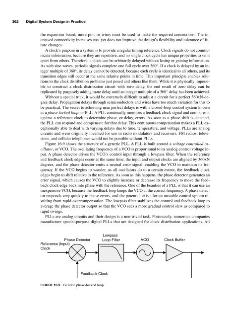
- Page 376 and 377: CHAPTER 16Clock DistributionClocks
- Page 378 and 379: Clock Distribution 357than common q
- Page 380 and 381: Clock Distribution 35950 MHzOscilla
- Page 384 and 385: Clock Distribution 363of the loop s
- Page 386 and 387: Clock Distribution 365Reference Clo
- Page 388 and 389: Clock Distribution 367delay-locked
- Page 390 and 391: Clock Distribution 369TransmitterCl
- Page 392 and 393: CHAPTER 17Voltage Regulation and Po
- Page 394 and 395: Voltage Regulation and Power Distri
- Page 396 and 397: Voltage Regulation and Power Distri
- Page 398 and 399: Voltage Regulation and Power Distri
- Page 400 and 401: Voltage Regulation and Power Distri
- Page 402 and 403: Voltage Regulation and Power Distri
- Page 404 and 405: Voltage Regulation and Power Distri
- Page 406 and 407: Voltage Regulation and Power Distri
- Page 408 and 409: Voltage Regulation and Power Distri
- Page 410 and 411: Voltage Regulation and Power Distri
- Page 412 and 413: Voltage Regulation and Power Distri
- Page 414 and 415: Voltage Regulation and Power Distri
- Page 416 and 417: Voltage Regulation and Power Distri
- Page 418 and 419: CHAPTER 18Signal IntegrityGetting h
- Page 420 and 421: Signal Integrity 399Z L - Z OΓ = -
- Page 422 and 423: Signal Integrity 401W = trace width
- Page 424 and 425: Signal Integrity 403cuits use 50-Ω
- Page 426 and 427: Signal Integrity 405make transmissi
- Page 428 and 429: Signal Integrity 40750 ΩZ O= 50 Ω
- Page 430 and 431: Signal Integrity 409copper traces.
- Page 432 and 433:
Signal Integrity 411Driver ICSignal
- Page 434 and 435:
Signal Integrity 413through the thi
- Page 436 and 437:
Signal Integrity 415node that all c
- Page 438 and 439:
Signal Integrity 417ICExternalConne
- Page 440 and 441:
CHAPTER 19Designing for SuccessA ho
- Page 442 and 443:
Designing for Success 421Manufactur
- Page 444 and 445:
Designing for Success 423Automated
- Page 446 and 447:
Designing for Success 425footprints
- Page 448 and 449:
Designing for Success 427directly t
- Page 450 and 451:
Designing for Success 429V CCV CC10
- Page 452 and 453:
Designing for Success 431AddressDec
- Page 454 and 455:
Designing for Success 433matching a
- Page 456 and 457:
Designing for Success 435matically
- Page 458 and 459:
Designing for Success 437are effect
- Page 460 and 461:
Designing for Success 439A 47-Ω se
- Page 462 and 463:
Designing for Success 4411-GHz digi
- Page 464 and 465:
APPENDIX AFurther EducationOne of t
- Page 466 and 467:
INDEX740074LS00 data sheet, 51-5474
- Page 468 and 469:
Index 447microprocessor with cache,
- Page 470 and 471:
Index 449data transmission, 107-108
- Page 472 and 473:
Index 451Ggain, see filterGAL, 252-
- Page 474 and 475:
Index 453general structure, 78in a
- Page 476 and 477:
Index 455PAL (programmable array lo
- Page 478 and 479:
Index 457semiconductor, 33, 293junc
- Page 480 and 481:
Index 459SRAM cell, 86switching reg