Enhanced field emission from O2 and CF4 plasma-treated CuO ...
Enhanced field emission from O2 and CF4 plasma-treated CuO ...
Enhanced field emission from O2 and CF4 plasma-treated CuO ...

You also want an ePaper? Increase the reach of your titles
YUMPU automatically turns print PDFs into web optimized ePapers that Google loves.
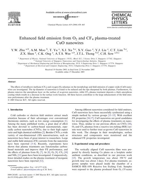
460 Y.W. Zhu et al. / Chemical Physics Letters 419 (2006) 458–463inset of Fig. 2c demonstrates clear crystalline structures,but the bottom right inset shows an amorphous layer witha thickness of 1–2 nm. On the cylindrical body of the nanowire,this amorphous layer becomes much thicker, evenmore than that of as-grown <strong>CuO</strong> nanowires.To investigate the chemical nature of the amorphouslayer on the surface of <strong>CuO</strong> nanowires after 10 min ofCF 4 RIE treatment, XPS study was carried out. The XPSspectra of F1s <strong>and</strong> Cu2p peaks are shown in Fig. 3a,b,respectively. From Fig. 3a, we can see that after CF 4<strong>plasma</strong> treatment, a strong two-peak F1s spectrumappears. By deconvoluting with Gaussian peaks after subtractionof background, four sub-peaks are furtherobserved. Those peaks at 684.7 <strong>and</strong> 685.7 eV can beascribed to the F–Cu bonding in CuF 2 <strong>and</strong> the other twoat 689.1 <strong>and</strong> 690.2 eV are possibly due to the presence of(–CF 2 –CF 2 –)n bonds [20]. The occurrence of fluorinatedcarbon <strong>and</strong> copper could be reasonably attributed to the10 min of CF 4 <strong>plasma</strong> treatment. Moreover, after CF 4<strong>plasma</strong> treatment (Fig. 3b), the Cu2p peaks tend to shiftto higher binding energy due to the formation of strongFig. 2. (a) TEM image of an as-grown <strong>CuO</strong> nanowire. The inset shows aHRTEM image <strong>from</strong> the tip part. (b) TEM image of a <strong>CuO</strong> nanowire afterexposure to 10 min of O 2 RIE. Insets are the HRTEM images of differentparts. (c) TEM image of a <strong>CuO</strong> nanowire after 10 min of CF 4 RIE.amorphous layers disappeared. From the insets of Fig. 2b,the crystalline structures are clearly seen to have extendedup to the surface. On the other h<strong>and</strong>, CF 4 <strong>plasma</strong> treatmentformed another amorphous layer coating onto thesurface as shown in Fig. 2c <strong>and</strong> its insets. The top rightFig. 3. XPS spectra of (a) F1s <strong>and</strong> (b) Cu2p for as-grown <strong>and</strong> CF 4<strong>plasma</strong>-<strong>treated</strong> <strong>CuO</strong> nanowires.
462 Y.W. Zhu et al. / Chemical Physics Letters 419 (2006) 458–463<strong>plasma</strong> can also generate copper superoxides (<strong>CuO</strong> x ,x = 2, 3, 4) which can improve the conductivity ofindium–tin oxide (ITO) [32]. Such improvements can alsoplay a role on the <strong>CuO</strong> nanowires after O 2 <strong>plasma</strong> treatment<strong>and</strong>, thus enhance their FE performance. Furthermore,<strong>plasma</strong> treatment may bombard <strong>and</strong> roughen thesurface of nanowires, thus producing new FE sites.In contrast, for the case of CF 4 <strong>plasma</strong> treatment, theFE enhancement may be more related to the fluorinatedcarbon layer on the nanowires after CF 4 <strong>plasma</strong> treatmentas was discussed in the XPS investigation. Previous studyhas shown that carbon coating on <strong>field</strong> emitters canenhance the <strong>field</strong> <strong>emission</strong> [33]. The dangling bonds willbe produced in the fluorinated carbon materials under highelectrical <strong>field</strong> [34], which can benefit the <strong>field</strong> <strong>emission</strong> [35].Such a fluorinated layer also results in a decrease in the surfacework function value. All these contribute to theenhanced <strong>field</strong> <strong>emission</strong> after 10 min of CF 4 <strong>plasma</strong> treatment,in addition to the larger <strong>emission</strong> density due to thinner<strong>and</strong> bent nanowires.4. ConclusionsO 2 <strong>and</strong> CF 4 <strong>plasma</strong> <strong>from</strong> RIE system have been used totreat aligned <strong>CuO</strong> nanowire films to enhance their FEproperties. Comparing the same nanowire before <strong>and</strong> aftertreatments shown that 10 min of <strong>plasma</strong> treatment reducesthe tip diameter of nanowires by an average of 9 nm. Furthermore,the nanowires tips sharpened <strong>and</strong>/or bent whichresult in a larger effective <strong>field</strong> <strong>emission</strong> area. O 2 <strong>plasma</strong>removed the amorphous layer on the surface of as-grownnanowires <strong>and</strong> CF 4 <strong>plasma</strong> induced fluorinated carbonon the surface of nanowires <strong>and</strong> reduced the work functionFig. 5. (a) Typical <strong>field</strong> <strong>emission</strong> J–E curves <strong>and</strong> FN plots (inset) of asgrown<strong>and</strong> O 2 <strong>plasma</strong>-<strong>treated</strong> <strong>CuO</strong> nanowires. (b) Typical <strong>field</strong> <strong>emission</strong>by about 0.5 eV. All these factors contributed to theJ–E curves <strong>and</strong> FN plots (inset) of as-grown <strong>and</strong> CF 4 <strong>plasma</strong>-<strong>treated</strong> <strong>CuO</strong> improved FE current density <strong>and</strong> lowered the turn-on <strong>field</strong>.nanowires.It is suggested that this <strong>plasma</strong> technique can also beextended to other nanomaterials, thus providing a directmeans to control the tip diameters <strong>and</strong> to functionalizeBy fitting the FN plots, the slopes <strong>and</strong> intercepts are obtained.Here, we add a subscript 0 to represent the results applications.the surface morphologies of nanowires for various<strong>from</strong> as-grown samples <strong>and</strong> 1 to represent those after10 min of <strong>plasma</strong> treatments. Thus, for both O 2 <strong>and</strong> CF 4 AcknowledgmentsRIE, the following relationships result <strong>from</strong> Eqs. (2) <strong>and</strong>(3): b 1b 06 1<strong>and</strong> a 1a 0 1, which suggest that after <strong>plasma</strong> The authors acknowledge the support <strong>from</strong> the Nationaltreatments, the enhanced FE may not be caused by the increasedaverage enhancement factors, but may be related to thanks the support <strong>from</strong> the Singapore MillenniumUniversity of Singapore Academic Research Fund. T. Yularger effective <strong>emission</strong> areas [29]. Actually, many nanowiresbecome bent after <strong>plasma</strong> treatments, which may in-Foundation.crease the effective FE <strong>emission</strong> area due to exposure of theReferencesside walls [17], as has been previously suggested for roughsurfaces [30].[1] A.A. Talin, K.A. Dean, J.E. Jaskie, Solid State Electron. 45 (2001)Another possible explanation for the enhanced FE after 963.O 2 <strong>plasma</strong> treatment is the cleaner surface structures. Previousresults have demonstrated that strong electron scat-(2004) 2239.[2] N. de Jonge, J.-M. Bonard, Phil. Trans. Roy. Soc., Lond. Ser. A 362[3] J. Zhou, N.S. Xu, S.Z. Deng, J. Chen, J.C. She, Z.L. Wang, Adv.tering can occur at the interface between the amorphousMater. 15 (2003) 1835.surface layer <strong>and</strong> crystalline core, which may encumber [4] J.J. Chiu, C.C. Kei, T.P. Perng, W.S. Wang, Adv. Mater. 15 (2003)the FE properties of as-grown <strong>CuO</strong> nanowires [31]. O 2 1361.
Y.W. Zhu et al. / Chemical Physics Letters 419 (2006) 458–463 463[5] C.J. Lee, T.J. Lee, S.C. Lyu, Y. Zhang, H. Ruh, H.J. Lee, Appl. Phys.Lett. 81 (2002) 3648.[6] Z.S. Wu, S.Z. Deng, N.S. Xu, J. Chen, J. Zhou, J. Chen, Appl. Phys.Lett. 80 (2002) 3829.[7] C.Y. Zhi, X.D. Bai, E.G. Wang, Appl. Phys. Lett. 81 (2002) 1690.[8] K.S. Ahn, J.S. Kim, C.O. Kim, J.P. Hong, Carbon 41 (2003) 2481.[9] S.C. Kung, K.C. Hwang, Appl. Phys. Lett. 80 (2002) 4819.[10] S.H. Lai, K.P. Huang, Y.M. Pan, Y.L. Chen, L.H. Chan, P. Lin,H.C. Shih, Chem. Phys. Lett. 382 (2003) 567.[11] J. Xu, J. Mei, X.H. Huang, X. Li, Z. Li, W. Li, K. Chen, Appl. Phys.A 80 (2004) 123.[12] F.C.K. Au, K.W. Wong, Y.H. Tang, Y.F. Zhang, I. Bello, S.T. Lee,Appl. Phys. Lett. 75 (1999) 1700.[13] T. Yu, X. Zhao, Z.X. Shen, Y.H. Wu, W.H. Su, J. Cryst. Growth 268(2004) 590.[14] X.C. Jiang, T. Herricks, Y.N. Xia, NanoLetters 2 (2002) 1333.[15] C.T. Hsieh, J.M. Chen, H.H. Lin, H.C. Shih, Appl. Phys. Lett. 82(2003) 3316.[16] C.T. Hsieh, J.M. Chen, H.H. Lin, H.C. Shih, Appl. Phys. Lett. 83(2003) 3383.[17] Y.W. Zhu, T. Yu, F.C. Cheong, X.J. Xu, C.T. Lim, V.B.C. Tan,J.T.L. Thong, C.H. Sow, Nanotechnology 16 (2005) 88.[18] Y.W. Zhu, F.C. Cheong, T. Yu, X.J. Xu, C.T. Lim, J.T.L. Thong, Z.X.Shen, C.K. Ong, Y.J. Liu, A.T.S. Wee, C.H. Sow, Carbon 43 (2005) 395.[19] K.Y. Lim, C.H. Sow, J. Lin, F.C. Cheong, Z.X. Shen, J.T.L. Thong,K.C. Chin, A.T.S. Wee, Adv. Mater. 15 (2003) 300.[20] C.D. Wagner, A.V. Naumkin, A.K. Vass, J.W. Allison, C.J. Powell,J.R. Rumble Jr, NIST X-ray Photoelectron Spectroscopy Database,Webversion:http://srdata.nist.gov/xps/.[21] H.F. Goldstein, D.S. Kim, P.Y. Yu, L.C. Bourne, Phys. Rev. B 41(1990) 7192.[22] H. Hagemam, H. Bill, W. Sadowski, E. Walker, M. François, SolidState Commun. 73 (1990) 467.[23] E.H. Lee, D.M. Hembree Jr, G.R. Rao, L.K. Mansur, Phys. Rev. B48 (1993) 15540.[24] Y. Park, V. Choong, Y. Gao, B.R. Hsieh, C.W. Tang, Appl. Phys.Lett. 68 (1996) 2699.[25] F.P. Koffyberg, F.A. Benko, J. Appl. Phys. 53 (1982) 1173.[26] H.H. Lin, C.Y. Wang, C.S. Han, J.M. Chen, C.T. Hsieh, J. Appl.Phys. 95 (2004) 5889.[27] R.H. Fowler, L.W. Nordheim, Proc. Roy. Soc., Lond. Ser. A 119(1928) 173.[28] I.S. Altman, P.V. Pikhitsa, M. Choi, Appl. Phys. Lett. 84 (2004) 1126.[29] D.A. Kirkpatrick, A. Mankofsky, K.T. Tsang, Appl. Phys. Lett. 60(1992) 2065.[30] R.C. Che, L.M. Peng, M.S. Wang, Appl. Phys. Lett. 85 (2004)4753.[31] Y.Z. Jin, W.K. Hsu, Y.L. Chueh, L.J. Chou, Y.Q. Zhu, K. Brigatti,H.W. Kroto, D.R.M. Walton, Angew. Chem., Int. Ed. 43 (2004)5670.[32] W. Hu, M. Matsumura, K. Furukawa, K. Torimitsu, J. Phys. Chem.B 108 (2004) 13116.[33] J. Liu, V.V. Zhirnov, A.F. Myers, G.J. Wojak, W.B. Choi, J.J. Hren,S.D. Wolter, M.T. McClure, B.R. Stoner, J.T. Glass, J. Vac. Sci.Technol. B 13 (1995) 442.[34] S.H. Lai, K.L. Chang, H.C. Shih, K.P. Huang, P. Lin, Appl. Phys.Lett. 85 (2004) 6248.[35] S. Han, J. Ihm, Phys. Rev. B 61 (2000) 9986.