Enhanced field emission from O2 and CF4 plasma-treated CuO ...
Enhanced field emission from O2 and CF4 plasma-treated CuO ...
Enhanced field emission from O2 and CF4 plasma-treated CuO ...

Create successful ePaper yourself
Turn your PDF publications into a flip-book with our unique Google optimized e-Paper software.
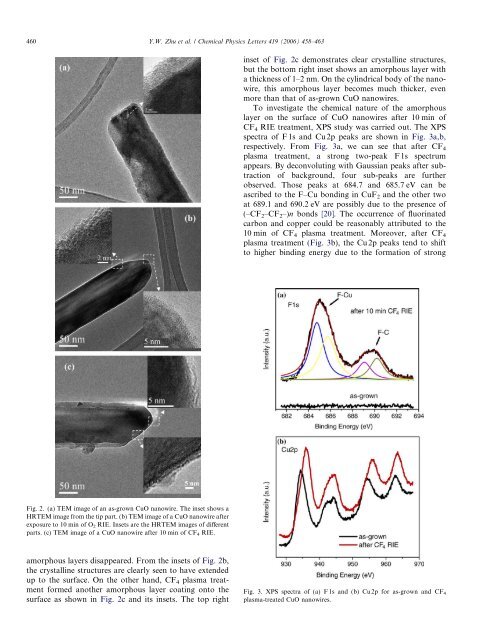
460 Y.W. Zhu et al. / Chemical Physics Letters 419 (2006) 458–463inset of Fig. 2c demonstrates clear crystalline structures,but the bottom right inset shows an amorphous layer witha thickness of 1–2 nm. On the cylindrical body of the nanowire,this amorphous layer becomes much thicker, evenmore than that of as-grown <strong>CuO</strong> nanowires.To investigate the chemical nature of the amorphouslayer on the surface of <strong>CuO</strong> nanowires after 10 min ofCF 4 RIE treatment, XPS study was carried out. The XPSspectra of F1s <strong>and</strong> Cu2p peaks are shown in Fig. 3a,b,respectively. From Fig. 3a, we can see that after CF 4<strong>plasma</strong> treatment, a strong two-peak F1s spectrumappears. By deconvoluting with Gaussian peaks after subtractionof background, four sub-peaks are furtherobserved. Those peaks at 684.7 <strong>and</strong> 685.7 eV can beascribed to the F–Cu bonding in CuF 2 <strong>and</strong> the other twoat 689.1 <strong>and</strong> 690.2 eV are possibly due to the presence of(–CF 2 –CF 2 –)n bonds [20]. The occurrence of fluorinatedcarbon <strong>and</strong> copper could be reasonably attributed to the10 min of CF 4 <strong>plasma</strong> treatment. Moreover, after CF 4<strong>plasma</strong> treatment (Fig. 3b), the Cu2p peaks tend to shiftto higher binding energy due to the formation of strongFig. 2. (a) TEM image of an as-grown <strong>CuO</strong> nanowire. The inset shows aHRTEM image <strong>from</strong> the tip part. (b) TEM image of a <strong>CuO</strong> nanowire afterexposure to 10 min of O 2 RIE. Insets are the HRTEM images of differentparts. (c) TEM image of a <strong>CuO</strong> nanowire after 10 min of CF 4 RIE.amorphous layers disappeared. From the insets of Fig. 2b,the crystalline structures are clearly seen to have extendedup to the surface. On the other h<strong>and</strong>, CF 4 <strong>plasma</strong> treatmentformed another amorphous layer coating onto thesurface as shown in Fig. 2c <strong>and</strong> its insets. The top rightFig. 3. XPS spectra of (a) F1s <strong>and</strong> (b) Cu2p for as-grown <strong>and</strong> CF 4<strong>plasma</strong>-<strong>treated</strong> <strong>CuO</strong> nanowires.