Enhanced field emission from O2 and CF4 plasma-treated CuO ...
Enhanced field emission from O2 and CF4 plasma-treated CuO ...
Enhanced field emission from O2 and CF4 plasma-treated CuO ...

Create successful ePaper yourself
Turn your PDF publications into a flip-book with our unique Google optimized e-Paper software.
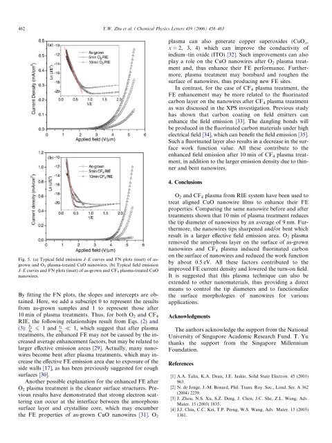
462 Y.W. Zhu et al. / Chemical Physics Letters 419 (2006) 458–463<strong>plasma</strong> can also generate copper superoxides (<strong>CuO</strong> x ,x = 2, 3, 4) which can improve the conductivity ofindium–tin oxide (ITO) [32]. Such improvements can alsoplay a role on the <strong>CuO</strong> nanowires after O 2 <strong>plasma</strong> treatment<strong>and</strong>, thus enhance their FE performance. Furthermore,<strong>plasma</strong> treatment may bombard <strong>and</strong> roughen thesurface of nanowires, thus producing new FE sites.In contrast, for the case of CF 4 <strong>plasma</strong> treatment, theFE enhancement may be more related to the fluorinatedcarbon layer on the nanowires after CF 4 <strong>plasma</strong> treatmentas was discussed in the XPS investigation. Previous studyhas shown that carbon coating on <strong>field</strong> emitters canenhance the <strong>field</strong> <strong>emission</strong> [33]. The dangling bonds willbe produced in the fluorinated carbon materials under highelectrical <strong>field</strong> [34], which can benefit the <strong>field</strong> <strong>emission</strong> [35].Such a fluorinated layer also results in a decrease in the surfacework function value. All these contribute to theenhanced <strong>field</strong> <strong>emission</strong> after 10 min of CF 4 <strong>plasma</strong> treatment,in addition to the larger <strong>emission</strong> density due to thinner<strong>and</strong> bent nanowires.4. ConclusionsO 2 <strong>and</strong> CF 4 <strong>plasma</strong> <strong>from</strong> RIE system have been used totreat aligned <strong>CuO</strong> nanowire films to enhance their FEproperties. Comparing the same nanowire before <strong>and</strong> aftertreatments shown that 10 min of <strong>plasma</strong> treatment reducesthe tip diameter of nanowires by an average of 9 nm. Furthermore,the nanowires tips sharpened <strong>and</strong>/or bent whichresult in a larger effective <strong>field</strong> <strong>emission</strong> area. O 2 <strong>plasma</strong>removed the amorphous layer on the surface of as-grownnanowires <strong>and</strong> CF 4 <strong>plasma</strong> induced fluorinated carbonon the surface of nanowires <strong>and</strong> reduced the work functionFig. 5. (a) Typical <strong>field</strong> <strong>emission</strong> J–E curves <strong>and</strong> FN plots (inset) of asgrown<strong>and</strong> O 2 <strong>plasma</strong>-<strong>treated</strong> <strong>CuO</strong> nanowires. (b) Typical <strong>field</strong> <strong>emission</strong>by about 0.5 eV. All these factors contributed to theJ–E curves <strong>and</strong> FN plots (inset) of as-grown <strong>and</strong> CF 4 <strong>plasma</strong>-<strong>treated</strong> <strong>CuO</strong> improved FE current density <strong>and</strong> lowered the turn-on <strong>field</strong>.nanowires.It is suggested that this <strong>plasma</strong> technique can also beextended to other nanomaterials, thus providing a directmeans to control the tip diameters <strong>and</strong> to functionalizeBy fitting the FN plots, the slopes <strong>and</strong> intercepts are obtained.Here, we add a subscript 0 to represent the results applications.the surface morphologies of nanowires for various<strong>from</strong> as-grown samples <strong>and</strong> 1 to represent those after10 min of <strong>plasma</strong> treatments. Thus, for both O 2 <strong>and</strong> CF 4 AcknowledgmentsRIE, the following relationships result <strong>from</strong> Eqs. (2) <strong>and</strong>(3): b 1b 06 1<strong>and</strong> a 1a 0 1, which suggest that after <strong>plasma</strong> The authors acknowledge the support <strong>from</strong> the Nationaltreatments, the enhanced FE may not be caused by the increasedaverage enhancement factors, but may be related to thanks the support <strong>from</strong> the Singapore MillenniumUniversity of Singapore Academic Research Fund. T. Yularger effective <strong>emission</strong> areas [29]. Actually, many nanowiresbecome bent after <strong>plasma</strong> treatments, which may in-Foundation.crease the effective FE <strong>emission</strong> area due to exposure of theReferencesside walls [17], as has been previously suggested for roughsurfaces [30].[1] A.A. Talin, K.A. Dean, J.E. Jaskie, Solid State Electron. 45 (2001)Another possible explanation for the enhanced FE after 963.O 2 <strong>plasma</strong> treatment is the cleaner surface structures. Previousresults have demonstrated that strong electron scat-(2004) 2239.[2] N. de Jonge, J.-M. Bonard, Phil. Trans. Roy. Soc., Lond. Ser. A 362[3] J. Zhou, N.S. Xu, S.Z. Deng, J. Chen, J.C. She, Z.L. Wang, Adv.tering can occur at the interface between the amorphousMater. 15 (2003) 1835.surface layer <strong>and</strong> crystalline core, which may encumber [4] J.J. Chiu, C.C. Kei, T.P. Perng, W.S. Wang, Adv. Mater. 15 (2003)the FE properties of as-grown <strong>CuO</strong> nanowires [31]. O 2 1361.