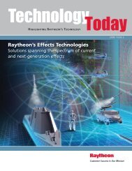
INTEGRATED MISSION SOLUTIONS DD(X ... - Raytheon
INTEGRATED MISSION SOLUTIONS DD(X ... - Raytheon
INTEGRATED MISSION SOLUTIONS DD(X ... - Raytheon

You also want an ePaper? Increase the reach of your titles
YUMPU automatically turns print PDFs into web optimized ePapers that Google loves.
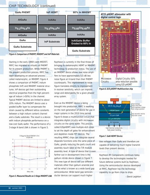
CHIP TECHNOLOGY (continued)<br />
Figure 4. Comparison of PHEMT, MHEMT and InP Materials<br />
Starting in the early 1990’s with MESFET,<br />
RRFC has migrated to virtually all PHEMT<br />
for its present production. While PHEMT is<br />
the present production process, RRFC has<br />
been developing an advanced process<br />
called metamorphic, or MHEMT. Figure 4<br />
shows a comparison of PHEMT, indium<br />
phosphide (InP) and MHEMT material structures.<br />
InP devices get their outstanding<br />
electrical properties from the high percentage<br />
of indium (>50%) in the channel.<br />
Typical PHEMT devices are limited to about<br />
20% indium. The MHEMT device uses a<br />
graded buffer layer to compensate the<br />
strain caused by different lattice constants<br />
between a high indium content channel<br />
and a GaAs substrate. The result is a device<br />
with indium phosphide performance on a<br />
low-cost GaAs wafer. The performance of a<br />
3-stage K-band LNA is shown in Figure 5.<br />
Figure 5. Measured Results on 3-Stage MHEMT LNA<br />
18 summer 2003<br />
<strong>Raytheon</strong> is currently in the final throes of<br />
bringing its metamorphic HEMT or MHEMT<br />
technology to production status. The use of<br />
an MHEMT device allows low noise amplifiers<br />
to have approximately 0.5 dB less<br />
noise figure at X-band than their PHEMT<br />
counterparts. This improvement in noise<br />
figure translates directly to improvement<br />
in receiver sensitivity, which can improve<br />
range and detectability for a given phased<br />
array system.<br />
Even as the MHEMT device is being<br />
brought into production, RRFC is working<br />
on the next generation of device for use in<br />
major systems in the 2010 time period.<br />
Figure 6 shows a multifunction circuit that<br />
integrates digital circuitry with microwave<br />
circuitry on the same wafer. This process,<br />
called E/DpHEMT, uses multiple etch stops<br />
to set the depth of gates for enhancement<br />
and depletion mode FET devices. The<br />
resulting MMIC chips can integrate several<br />
disparate functions onto the same piece of<br />
GaAs, greatly reducing the parts count and<br />
assembly touch labor at the T/R module<br />
assembly level. A type of device that is even<br />
farther out in development time is the<br />
gallium nitride device shown in Figure 7.<br />
This new type of device will use different<br />
materials other than gallium arsenide and<br />
will be what is known as a wide band gap<br />
semiconductor. Wide band gap semiconductor<br />
devices can support much higher<br />
AT25 pHEMT attenuator with<br />
digital control logic<br />
Microwave<br />
Circuitry<br />
Digital Circuitry 50%<br />
area reduction possible<br />
using E/D pHEMT<br />
Figure 6. E/D pHEMT Multifunction chip<br />
300 Å i-Al 0.2 Ga 0.8 N<br />
i-AlGaN Spacer<br />
0.3 µm i-GaN<br />
0.1 µm AlN Buffer<br />
SiC Substrate<br />
high thermal conductivity<br />
high power handling<br />
Figure 7. GaN HEMT Device<br />
large bandgap<br />
large critical field<br />
high breakdown voltage<br />
high voltage operation<br />
high saturation velocity<br />
high drain current<br />
bias voltages than GaAs and therefore are<br />
capable of delivering much higher transmit<br />
levels than present devices.<br />
<strong>Raytheon</strong> RF Components continues today<br />
to develop the technologies needed for<br />
future defense systems built by <strong>Raytheon</strong>.<br />
Using the semiconductor devices developed<br />
at RRFC, <strong>Raytheon</strong> has the technology<br />
capability to go from chips to ships.<br />
- David Laighton