IPM 09 (Rev. 3)
IPM 09 (Rev. 3)
IPM 09 (Rev. 3)

You also want an ePaper? Increase the reach of your titles
YUMPU automatically turns print PDFs into web optimized ePapers that Google loves.
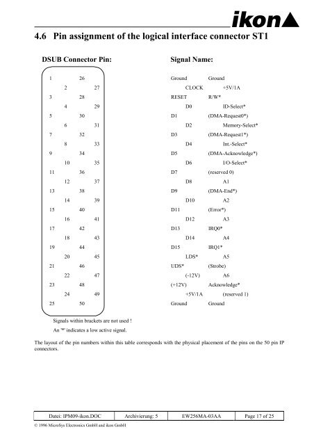
4.6 Pin assignment of the logical interface connector ST1<br />
DSUB Connector Pin: Signal Name:<br />
1 26 Ground Ground<br />
2 27 CLOCK +5V/1A<br />
3 28 RESET R/W*<br />
4 29 D0 ID-Select*<br />
5 30 D1 (DMA-Request0*)<br />
6 31 D2 Memory-Select*<br />
7 32 D3 (DMA-Request1*)<br />
8 33 D4 Int.-Select*<br />
9 34 D5 (DMA-Acknowledge*)<br />
10 35 D6 I/O-Select*<br />
11 36 D7 (reserved 0)<br />
12 37 D8 A1<br />
13 38 D9 (DMA-End*)<br />
14 39 D10 A2<br />
15 40 D11 (Error*)<br />
16 41 D12 A3<br />
17 42 D13 IRQ0*<br />
18 43 D14 A4<br />
19 44 D15 IRQ1*<br />
20 45 LDS* A5<br />
21 46 UDS* (Strobe)<br />
22 47 (-12V) A6<br />
23 48 (+12V) Acknowledge*<br />
24 49 +5V/1A (reserved 1)<br />
25 50 Ground Ground<br />
Signals within brackets are not used !<br />
An '*' indicates a low active signal.<br />
The layout of the pin numbers within this table corresponds with the physical placement of the pins on the 50 pin IP<br />
connectors.<br />
Datei: <strong>IPM</strong><strong>09</strong>-ikon.DOC Archivierung: 5 EW256MA-03AA Page 17 of 25<br />
© 1996 MicroSys Electronics GmbH and ikon GmbH