Microstructure and magnetic properties of FePt and Fe/FePt ...
Microstructure and magnetic properties of FePt and Fe/FePt ...
Microstructure and magnetic properties of FePt and Fe/FePt ...

You also want an ePaper? Increase the reach of your titles
YUMPU automatically turns print PDFs into web optimized ePapers that Google loves.
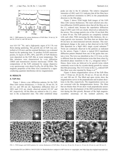
476 J. Appl. Phys., Vol. 96, No. 1, 1 July 2004 Takahashi et al.FIG. 1. XRD patterns for various thicknesses <strong>of</strong> <strong><strong>Fe</strong>Pt</strong> films: 10 nm a, 30nm b, 38nmc, <strong>and</strong> 100 nm d.was 6.010 7 Pa, <strong>and</strong> a high-purity argon <strong>of</strong> 0.1 Pa wasflown during sputtering. The growth rate <strong>of</strong> <strong><strong>Fe</strong>Pt</strong> was controlledto 0.10 nm/s <strong>and</strong> the nominal thickness was evaluatedbased on the sputtering time. To produce <strong>Fe</strong>/<strong><strong>Fe</strong>Pt</strong> nanocomposites,<strong>Fe</strong> layers <strong>of</strong> 20%, 40%, <strong>and</strong> 60% <strong>of</strong> <strong><strong>Fe</strong>Pt</strong> thicknesswere deposited on the <strong><strong>Fe</strong>Pt</strong> film at room temperature. Thefilm structures were characterized by x-ray diffractionXRD <strong>and</strong> transmission electron microscopy TEM. Thecompositions <strong>of</strong> the <strong><strong>Fe</strong>Pt</strong> estimated by energy dispersivex-ray spectroscopy were about <strong>Fe</strong> 50 Pt 50 for all the films. The<strong>magnetic</strong> <strong>properties</strong> <strong>of</strong> the films were examined by a superconductingquantum interference device magnetometer.III. RESULTSA. <strong><strong>Fe</strong>Pt</strong> filmFigure 1 shows x-ray diffraction patterns for the <strong><strong>Fe</strong>Pt</strong>films with various thicknesses, t10 nm a, 30nmb, 38nm c, <strong>and</strong> 100 nm d. Superlattice diffraction lines <strong>of</strong>001 <strong>and</strong> 112 are clearly observed around 224° <strong>and</strong>60°, respectively. All the films are ordered to the L1 0 structurein the as-deposited state. The other unlabeled sharppeaks are due to the Si substrate. The relative integratedintensities <strong>of</strong> 001 <strong>and</strong> 111 indicates that all the films havea weak preferred orientation to 001 in the perpendiculardirection to the film plane.Figure 2 shows TEM bright field images <strong>of</strong> the <strong><strong>Fe</strong>Pt</strong>films with various thicknesses. The inset selected area electrondiffraction SAED patterns show that all the films are inthe L1 0 ordered state, because the superlattice diffractionrings <strong>of</strong> 001 <strong>and</strong> 110 are clearly observed as indicated bythe arrows. The average particle size <strong>of</strong> the 10 nm thick filmis about 50 nm. The <strong><strong>Fe</strong>Pt</strong> particles are completely isolatedwith each other. With increasing the film thickness, the averageparticle size increases. The films that are thicker than60 nm have an interconnected network structure. This morphologicalchange is the same as that observed in the <strong><strong>Fe</strong>Pt</strong>film deposited on a MgO 001 single crystal substrate. 14Twins are commonly observed in the particles as indicatedby the arrows. Figure 3 shows a typical 011 nanobeamdiffraction pattern obtained from one <strong>of</strong> the grains that containa twin. The twin was identified as the (111¯) twin, so thisis different from the transformation twins that form when fccdisordered phase transform to the L1 0 tetragonal lattice. 18Hence, these twins are believed to be growth twins whichcommonly occur in the fcc crystals during growth by variousthin film processing. The 111 twins in the L1 0 ordered <strong><strong>Fe</strong>Pt</strong>thin films were also reported by Hong et al. 19Figure 4 shows magnetization curves <strong>of</strong> the <strong><strong>Fe</strong>Pt</strong> filmswith t10 nm a, 20nmb, 30nmc, 38nmd, 60nme, <strong>and</strong> 100 nm f. The filled <strong>and</strong> open circles show themagnetization curves in the perpendicular <strong>and</strong> in-plane directionsto the film, respectively. The magnetization curves arenot corrected with the demagnetization factors. The filmsthat are thicker than 30 nm show weak perpendicular anisotropydue to the development <strong>of</strong> the 001 preferred orientationduring the film growth. Because <strong>of</strong> the high magnetocrystallineanisotropy <strong>of</strong> the isolated particles, theFIG. 2. TEM images <strong>and</strong> SAED patterns for various thicknesses <strong>of</strong> <strong><strong>Fe</strong>Pt</strong> films: 10 nm a, 20nmb, 30nmc, 38nmd, 60nme, <strong>and</strong> 100 nm f.Downloaded 26 Jun 2004 to 144.213.253.14. Redistribution subject to AIP license or copyright, see http://jap.aip.org/jap/copyright.jsp