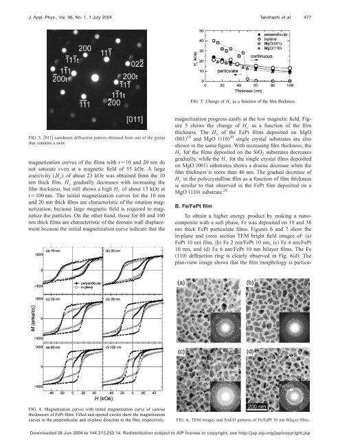
476 J. Appl. Phys., Vol. 96, No. 1, 1 July 2004 Takahashi et al.FIG. 1. XRD patterns for various thicknesses <strong>of</strong> <strong><strong>Fe</strong>Pt</strong> films: 10 nm a, 30nm b, 38nmc, <strong>and</strong> 100 nm d.was 6.010 7 Pa, <strong>and</strong> a high-purity argon <strong>of</strong> 0.1 Pa wasflown during sputtering. The growth rate <strong>of</strong> <strong><strong>Fe</strong>Pt</strong> was controlledto 0.10 nm/s <strong>and</strong> the nominal thickness was evaluatedbased on the sputtering time. To produce <strong>Fe</strong>/<strong><strong>Fe</strong>Pt</strong> nanocomposites,<strong>Fe</strong> layers <strong>of</strong> 20%, 40%, <strong>and</strong> 60% <strong>of</strong> <strong><strong>Fe</strong>Pt</strong> thicknesswere deposited on the <strong><strong>Fe</strong>Pt</strong> film at room temperature. Thefilm structures were characterized by x-ray diffractionXRD <strong>and</strong> transmission electron microscopy TEM. Thecompositions <strong>of</strong> the <strong><strong>Fe</strong>Pt</strong> estimated by energy dispersivex-ray spectroscopy were about <strong>Fe</strong> 50 Pt 50 for all the films. The<strong>magnetic</strong> <strong>properties</strong> <strong>of</strong> the films were examined by a superconductingquantum interference device magnetometer.III. RESULTSA. <strong><strong>Fe</strong>Pt</strong> filmFigure 1 shows x-ray diffraction patterns for the <strong><strong>Fe</strong>Pt</strong>films with various thicknesses, t10 nm a, 30nmb, 38nm c, <strong>and</strong> 100 nm d. Superlattice diffraction lines <strong>of</strong>001 <strong>and</strong> 112 are clearly observed around 224° <strong>and</strong>60°, respectively. All the films are ordered to the L1 0 structurein the as-deposited state. The other unlabeled sharppeaks are due to the Si substrate. The relative integratedintensities <strong>of</strong> 001 <strong>and</strong> 111 indicates that all the films havea weak preferred orientation to 001 in the perpendiculardirection to the film plane.Figure 2 shows TEM bright field images <strong>of</strong> the <strong><strong>Fe</strong>Pt</strong>films with various thicknesses. The inset selected area electrondiffraction SAED patterns show that all the films are inthe L1 0 ordered state, because the superlattice diffractionrings <strong>of</strong> 001 <strong>and</strong> 110 are clearly observed as indicated bythe arrows. The average particle size <strong>of</strong> the 10 nm thick filmis about 50 nm. The <strong><strong>Fe</strong>Pt</strong> particles are completely isolatedwith each other. With increasing the film thickness, the averageparticle size increases. The films that are thicker than60 nm have an interconnected network structure. This morphologicalchange is the same as that observed in the <strong><strong>Fe</strong>Pt</strong>film deposited on a MgO 001 single crystal substrate. 14Twins are commonly observed in the particles as indicatedby the arrows. Figure 3 shows a typical 011 nanobeamdiffraction pattern obtained from one <strong>of</strong> the grains that containa twin. The twin was identified as the (111¯) twin, so thisis different from the transformation twins that form when fccdisordered phase transform to the L1 0 tetragonal lattice. 18Hence, these twins are believed to be growth twins whichcommonly occur in the fcc crystals during growth by variousthin film processing. The 111 twins in the L1 0 ordered <strong><strong>Fe</strong>Pt</strong>thin films were also reported by Hong et al. 19Figure 4 shows magnetization curves <strong>of</strong> the <strong><strong>Fe</strong>Pt</strong> filmswith t10 nm a, 20nmb, 30nmc, 38nmd, 60nme, <strong>and</strong> 100 nm f. The filled <strong>and</strong> open circles show themagnetization curves in the perpendicular <strong>and</strong> in-plane directionsto the film, respectively. The magnetization curves arenot corrected with the demagnetization factors. The filmsthat are thicker than 30 nm show weak perpendicular anisotropydue to the development <strong>of</strong> the 001 preferred orientationduring the film growth. Because <strong>of</strong> the high magnetocrystallineanisotropy <strong>of</strong> the isolated particles, theFIG. 2. TEM images <strong>and</strong> SAED patterns for various thicknesses <strong>of</strong> <strong><strong>Fe</strong>Pt</strong> films: 10 nm a, 20nmb, 30nmc, 38nmd, 60nme, <strong>and</strong> 100 nm f.Downloaded 26 Jun 2004 to 144.213.253.14. Redistribution subject to AIP license or copyright, see http://jap.aip.org/jap/copyright.jsp
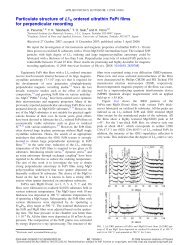
J. Appl. Phys., Vol. 96, No. 1, 1 July 2004 Takahashi et al.477FIG. 5. Change <strong>of</strong> H c as a function <strong>of</strong> the film thickness.FIG. 3. 011 nanobeam diffraction pattern obtained from one <strong>of</strong> the grainsthat contains a twin.magnetization curves <strong>of</strong> the films with t10 <strong>and</strong> 20 nm donot saturate even at a <strong>magnetic</strong> field <strong>of</strong> 55 kOe. A largecoercivity (H c ) <strong>of</strong> about 23 kOe was obtained from the 10nm thick film. H c gradually decreases with increasing thefilm thickness, but still shows a high H c <strong>of</strong> about 13 kOe att100 nm. The initial magnetization curves for the 10 nm<strong>and</strong> 20 nm thick films are characteristic <strong>of</strong> the rotation magnetization,because large <strong>magnetic</strong> field is required to magnetizethe particles. On the other h<strong>and</strong>, those for 60 <strong>and</strong> 100nm thick films are characteristic <strong>of</strong> the domain wall displacementbecause the initial magnetization curve indicate that themagnetization progress easily at the low <strong>magnetic</strong> field. Figure5 shows the change <strong>of</strong> H c as a function <strong>of</strong> the filmthickness. The H c <strong>of</strong> the <strong><strong>Fe</strong>Pt</strong> films deposited on MgO001 14 <strong>and</strong> MgO 110 20 single crystal substrates are alsoshown in the same figure. With increasing film thickness, theH c for the films deposited on the SiO 2 substrates decreasesgradually, while the H c for the single crystal films depositedon MgO 001 substrates shows a drastic decrease when thefilm thickness is more than 40 nm. The gradual decrease <strong>of</strong>H c in the polycrystalline film as a function <strong>of</strong> film thicknessis similar to that observed in the <strong><strong>Fe</strong>Pt</strong> film deposited on aMgO 110 substrate. 20B. <strong>Fe</strong>Õ<strong><strong>Fe</strong>Pt</strong> filmTo obtain a higher energy product by making a nanocompositewith a s<strong>of</strong>t phase, <strong>Fe</strong> was deposited on 10 <strong>and</strong> 38nm thick <strong><strong>Fe</strong>Pt</strong> particulate films. Figures 6 <strong>and</strong> 7 show thein-plane <strong>and</strong> cross section TEM bright field images <strong>of</strong>: a<strong><strong>Fe</strong>Pt</strong> 10 nm film, b <strong>Fe</strong> 2 nm/<strong><strong>Fe</strong>Pt</strong> 10 nm, c <strong>Fe</strong> 4 nm/<strong><strong>Fe</strong>Pt</strong>10 nm, <strong>and</strong> d <strong>Fe</strong> 6 nm/<strong><strong>Fe</strong>Pt</strong> 10 nm bilayer films. The <strong>Fe</strong>110 diffraction ring is clearly observed in Fig. 6d. Theplan-view image shows that the film morphology is particu-FIG. 4. Magnetization curves with initial magnetization curve <strong>of</strong> variousthicknesses <strong>of</strong> <strong><strong>Fe</strong>Pt</strong> films. Filled <strong>and</strong> opened circles show the magnetizationcurves in the perpendicular <strong>and</strong> in-plane direction to the film, respectively.FIG. 6. TEM images <strong>and</strong> SAED patterns <strong>of</strong> <strong>Fe</strong>/<strong><strong>Fe</strong>Pt</strong> 10 nm bilayer films.Downloaded 26 Jun 2004 to 144.213.253.14. Redistribution subject to AIP license or copyright, see http://jap.aip.org/jap/copyright.jsp