Crystal growth and defects
Crystal growth and defects
Crystal growth and defects

Create successful ePaper yourself
Turn your PDF publications into a flip-book with our unique Google optimized e-Paper software.
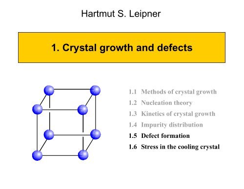
Hartmut S. Leipner<br />
1. <strong>Crystal</strong> <strong>growth</strong> <strong>and</strong> <strong>defects</strong><br />
1.1 Methods of crystal <strong>growth</strong><br />
1.2 Nucleation theory<br />
1.3 Kinetics of crystal <strong>growth</strong><br />
1.4 Impurity distribution<br />
1.5 Defect formation<br />
1.6 Stress in the cooling crystal
1.5 Defect formation<br />
Misfit dislocations<br />
Lattice constants<br />
hsl 2002 – Structure of imperfect crystals 2 – <strong>Crystal</strong> <strong>growth</strong> <strong>and</strong> defect formation Strained layer 2<br />
a +<br />
a<br />
a
¡<br />
¡<br />
¡<br />
Misfit dislocations <strong>and</strong> <strong>growth</strong><br />
Misfit between regions of different compositions (impurities, dopants)<br />
resulting in a change in the lattice constant<br />
Misfit at boundaries of <strong>growth</strong> pyramids or facets during non-planar<br />
<strong>growth</strong><br />
Simple case of constant concentration gradient gives two<br />
perpendicular sets of edge dislocations with a density<br />
£<br />
¤<br />
¥ b grad c<br />
( ¢ linear expansion coefficient related to the concentration c,<br />
b magnitude of the Burgers vector)<br />
hsl 2002 – Structure of imperfect crystals 2 – <strong>Crystal</strong> <strong>growth</strong> <strong>and</strong> defect formation 3
In-grown dislocations<br />
¦ Propagation of dislocation during <strong>growth</strong>: a dislocation ending on the<br />
<strong>growth</strong> face will proceed with the growing crystal<br />
¦ Spiral <strong>growth</strong> connected with screw dislocations<br />
¦ Sources of dislocations: Inclusions, gas bubbles, precipitates<br />
¦ Grown-in dislocations frequently found in non-crystallographic<br />
directions, which depend on the <strong>growth</strong> direction<br />
¦ Post-<strong>growth</strong> movement of dislocations leads to irregular dislocation<br />
networks, cell structure<br />
hsl 2002 – Structure of imperfect crystals 2 – <strong>Crystal</strong> <strong>growth</strong> <strong>and</strong> defect formation 4
Propagation of dislocations<br />
(a) g g<br />
g<br />
g (b)<br />
X-ray topography of grown-in dislocations. a) Propagation of dislocations<br />
from the seed in a Czochralski benzophenone crystal. b) Czochralski salol<br />
containing tiny gas bubbles <strong>and</strong> numerous dislocations starting from them.<br />
The length of the imaged crystals is about 46 mm, the thickness 1.2 mm.<br />
g is the diffraction vector; CuK ¢ radiation.<br />
[Klapper 1996]<br />
hsl 2002 – Structure of imperfect crystals 2 – <strong>Crystal</strong> <strong>growth</strong> <strong>and</strong> defect formation 6<br />
Grown-in dislocations
¦<br />
¦<br />
¦<br />
¦<br />
¦<br />
<strong>Crystal</strong>s with a low dislocation density<br />
Start of the <strong>growth</strong> at the seed very critical <strong>and</strong> a high density of<br />
extended <strong>defects</strong> (dislocations, small-angle grain boundaries) is formed<br />
“Neck-<strong>and</strong>-shoulder” technique<br />
Remaining dislocation density usually 10 2 to 10 3 cm −2<br />
Dislocation-free Si as a routine technology (avoid new formation of<br />
dislocations – no foreign phases, stress-free <strong>growth</strong>!)<br />
Si not defect-free, in addition to point <strong>defects</strong> it contains micro<strong>defects</strong><br />
(e. g. swirls)<br />
hsl 2002 – Structure of imperfect crystals 2 – <strong>Crystal</strong> <strong>growth</strong> <strong>and</strong> defect formation 7
Extension of dislocations from the seed<br />
X-ray topography of dislocations <strong>and</strong> micro<strong>defects</strong>.<br />
A cross section of the neck region of a silicon crystal<br />
is shown. The seed was located above.<br />
[Bohm 1995]<br />
Growth direction<br />
hsl 2002 – Structure of imperfect crystals 2 – <strong>Crystal</strong> <strong>growth</strong> <strong>and</strong> defect formation Seed 8
Micro<strong>defects</strong> in dislocation-free silicon<br />
a) b)<br />
a) A swirl in floating-zone material, b) microdefect in Czochralski silicon.<br />
TEM bright field, 1 MV.<br />
[Gleichmann et al. 1987]<br />
hsl 2002 – Structure of imperfect crystals 2 – <strong>Crystal</strong> <strong>growth</strong> <strong>and</strong> defect formation Microdefect silicon 9<br />
A swirl
Condensation of point <strong>defects</strong><br />
Dislocation formation by condensation of vacancies<br />
hsl 2002 – Structure of imperfect crystals 2 – <strong>Crystal</strong> <strong>growth</strong> <strong>and</strong> defect formation Vacancy loop [Wilke:88]<br />
10
§<br />
§<br />
§<br />
§<br />
§<br />
Density of loops<br />
Parameters: supersaturation of point <strong>defects</strong>, diffusion coefficient,<br />
cooling time<br />
Maximum density of dislocations according to Schoeck, Tiller<br />
(1960)<br />
(c 0 , c point defect concentration at melting point <strong>and</strong> at the given<br />
temperature, r loop radius)<br />
Quantitative estimations however difficult<br />
Not only agglomeration of point <strong>defects</strong> – such loops are sinks for<br />
other supersaturated <strong>defects</strong><br />
Further <strong>growth</strong> or shrinking; gettering of impurities<br />
¨©<br />
c 0 � c<br />
2rb<br />
hsl 2002 – Structure of imperfect crystals 2 – <strong>Crystal</strong> <strong>growth</strong> <strong>and</strong> defect formation 11
Gettering<br />
Dot–halo cathodoluminescence contrast as manifestation of the<br />
immobilization of in-grown dislocations by gettering of point <strong>defects</strong><br />
hsl 2002 – Structure of imperfect crystals 2 – <strong>Crystal</strong> <strong>growth</strong> <strong>and</strong> defect formation Halo, SEM 9897 n-GaAs<br />
12
� Grain boundaries<br />
Two-dimensional <strong>defects</strong><br />
polycrystalline <strong>growth</strong>; parasitic nucleation <strong>and</strong> merging of crystal<br />
parts<br />
� Small-angle boundaries<br />
grown-in; misfit; plastic deformation*<br />
� Twins <strong>and</strong> stacking faults<br />
grown-in; plastic deformation* <strong>and</strong> dissociation of perfect<br />
dislocations; phase transitions<br />
� Antiphase boundaries <strong>and</strong> domains<br />
phase transitions; spontaneous change in the orientation;<br />
non-stoichiometry<br />
* induced by strain during <strong>growth</strong>/cooling<br />
hsl 2002 – Structure of imperfect crystals 2 – <strong>Crystal</strong> <strong>growth</strong> <strong>and</strong> defect formation 13
Inclusion of a foreign phase<br />
� Coarse perturbation of homogeneity of a growing crystal<br />
� Precipitation of a foreign phase; interaction with the defect<br />
structure of the crystal<br />
� Micro<strong>defects</strong> only in dislocation-free (parts of) crystals,<br />
otherwise segregation at dislocations<br />
� Temperature regime after crystallization important;<br />
quenching would be favorable to avoid precipitation, but<br />
thermal strain induces dislocations<br />
� Capture of foreign phases: gas bubbles, inclusion of the<br />
solvent, impurities from the crucible<br />
hsl 2002 – Structure of imperfect crystals 2 – <strong>Crystal</strong> <strong>growth</strong> <strong>and</strong> defect formation 14
Interaction of precipitation <strong>and</strong> dislocations<br />
0.1 mm<br />
Precipitates in GGG (g<strong>and</strong>olinium gallium granate Gd 3 Ga 5 O 12 )<br />
[Wilke 1988/Bohm 1977]<br />
hsl 2002 – Structure of imperfect crystals 2 – <strong>Crystal</strong> <strong>growth</strong> <strong>and</strong> defect formation GGG 15
1.6 Strain in the cooling crystal<br />
Sources of strain<br />
�<br />
�<br />
�<br />
Gravity<br />
axial stress up to 0.05 MPa for a 500 mm long crystal<br />
Interaction with containers<br />
good condition if wetting can be avoided;<br />
if the crystal sticks to the container, different thermal expansion<br />
coefficients may give rise to enormous forces (brittle fracture)<br />
Stress induced by inhomogeneities<br />
striations, inclusions<br />
hsl 2002 – Structure of imperfect crystals 2 – <strong>Crystal</strong> <strong>growth</strong> <strong>and</strong> defect formation 16
Heat transfer during <strong>growth</strong><br />
Schematic visualization of heat<br />
exchange processes during LEC<br />
<strong>growth</strong><br />
hsl 2002 – Structure of imperfect crystals 2 – <strong>Crystal</strong> <strong>growth</strong> <strong>and</strong> defect formation Growth heat transfer [Völkl:94]<br />
18
Concept of critical resolved shear stress<br />
� CRSS – threshold value for plastic deformation of the crystal<br />
� Wherever the elastic stress, obtained from the temperature field<br />
calculated, exceeds this critical value, plastic deformation occurs<br />
� No differentiation between dislocation nucleation <strong>and</strong> multiplication,<br />
only qualitative estimations<br />
� Main criticism of Alex<strong>and</strong>er: not the existence of an unlocking stress<br />
for dislocation mobilization, but neglecting the time dependence:<br />
dislocation density is a function of the whole thermal <strong>and</strong> stress<br />
history of the crystal<br />
hsl 2002 – Structure of imperfect crystals 2 – <strong>Crystal</strong> <strong>growth</strong> <strong>and</strong> defect formation 19
Model of dislocation multiplication<br />
Alex<strong>and</strong>er-Haasen model of plastic deformation<br />
�<br />
�<br />
�<br />
Concept of effective stress, which is needed for a dislocation to overcome<br />
the lattice resistance<br />
� = � eff = � a<br />
hsl 2002 – Structure of imperfect crystals 2 – <strong>Crystal</strong> <strong>growth</strong> <strong>and</strong> defect formation 20<br />
− � i<br />
Stress due to the interaction of moving dislocations<br />
( � m density of mobile dislocations, D 0 strain hardening factor,<br />
Dislocation velocity v<br />
v � v 0<br />
� i<br />
� Gb<br />
� a � D 0<br />
� m<br />
� 0<br />
� m<br />
�<br />
� D0<br />
� m<br />
m<br />
exp �<br />
Q<br />
k B T<br />
� interaction factor)
�<br />
�<br />
�<br />
�<br />
Alex<strong>and</strong>er–Haasen model<br />
Dislocation multiplication law<br />
d � m<br />
Orowan equation<br />
� a �<br />
� m b v �<br />
Slip a related via Schmid factor to (plastic) strain �<br />
� a �<br />
���<br />
� K � eff<br />
The constants for GaAs: m = 1.7,<br />
� 0 = 1 MPa, K = 7×10⁻³ m/N, D0 = 3.12 N/m<br />
[Tsai et al. 1993]<br />
�<br />
�� tot �<br />
�<br />
� m v d t �<br />
� m b v 0<br />
�� elast<br />
� m K v 0<br />
� a � D 0<br />
� m<br />
� 0<br />
� a � D 0<br />
� m<br />
� = 1, Q = 1.4 eV, v0 = 1.8×10⁸ m/s,<br />
hsl 2002 – Structure of imperfect crystals 2 – <strong>Crystal</strong> <strong>growth</strong> <strong>and</strong> defect formation 21<br />
m �<br />
� 0<br />
� exp �<br />
m �<br />
Q<br />
k B T<br />
� exp �<br />
Q<br />
k B T<br />
d t
Growth axis z<br />
010<br />
Thermal elasticity model<br />
� 1 1 0<br />
�<br />
�<br />
�<br />
�<br />
Thermal stress calculations in cylindrical<br />
coordinates<br />
Assuming isotropic material <strong>and</strong> axisymmetric<br />
crystal<br />
Two-dimensional thermal elasticity model<br />
Thermal elastic stress components � rr , ���<br />
� , � zz, � rz<br />
� transformation to each slip system to simulate<br />
dislocation motion/multiplication<br />
hsl 2002 – Structure of imperfect crystals 2 – <strong>Crystal</strong> <strong>growth</strong> <strong>and</strong> defect formation 22
5 mm<br />
Isotherms in a growing crystal<br />
T (K)<br />
12/18<br />
Boric oxide Nitrogen<br />
T (K)<br />
30/44<br />
Isotherms in InP crystals grown under 12/18 <strong>and</strong> 30/44 conditions denoting<br />
the initial/final boric oxide heights in mm. An additional afterheater was<br />
used to increase the temperature in the gas atmosphere in the 30/44 crystal.<br />
[Völkl 1994]<br />
hsl 2002 – Structure of imperfect crystals 2 – <strong>Crystal</strong> <strong>growth</strong> <strong>and</strong> defect formation InP crystal isotherms 23<br />
Boric oxide Nitrogen
�<br />
�<br />
�<br />
�<br />
�<br />
Thermoelastic stress<br />
Inhomogeneous temperature distribution coupled with locally different<br />
expansion/contraction<br />
Resulting strain converted into stresses via Hooke’s law<br />
Assuming completely elastic behavior over the whole temperature range !<br />
Theory of thermoelasticity<br />
see e. g. Timoshenko: Theory of elasticity (1951)<br />
Simple rules:<br />
i. Temperature field which is linear in all coordinates results in a stress-free<br />
state (free temperature bending)<br />
ii. Scaling of dimensions <strong>and</strong> temperature differences<br />
iii. Incompatibilities of the temperature field are sources of stress<br />
hsl 2002 – Structure of imperfect crystals 2 – <strong>Crystal</strong> <strong>growth</strong> <strong>and</strong> defect formation 24
� vM<br />
�<br />
Von Mises stress<br />
� rr �<br />
� zz<br />
2 �<br />
� zz �<br />
���<br />
Contour plots of the von Mises<br />
stress (in MPa) for the <strong>growth</strong><br />
conditions of 12/18 <strong>and</strong> 30/44 InP<br />
crystals<br />
[Völkl 1994]<br />
hsl 2002 – Structure of imperfect crystals 2 – <strong>Crystal</strong> <strong>growth</strong> <strong>and</strong> defect formation von Mises stress 25<br />
�<br />
2<br />
2 �<br />
� �<br />
�<br />
�<br />
� rr<br />
�<br />
2 2 �<br />
6 rz
Resolved shear stress<br />
� Glide forces on dislocations has to be calculated for in each slip<br />
system<br />
�<br />
fcc structure: 12 systems of the type 1 0 � { 111 }<br />
� Peach–Koehler equation for the force per unit dislocation length<br />
� The glide force is the projection of F in the slip plane, perpendicular<br />
to the dislocation<br />
� Resolved shear stress � = Fg/b<br />
F � b �<br />
F g<br />
hsl 2002 – Structure of imperfect crystals 2 – <strong>Crystal</strong> <strong>growth</strong> <strong>and</strong> defect formation 26<br />
� F � n<br />
� l<br />
�<br />
1<br />
� l
Dislocation multiplication during <strong>growth</strong><br />
Rate of dislocation multiplication related to the <strong>growth</strong> velocity v gr<br />
m (cm −2 )<br />
�<br />
e Result of numerical<br />
calculations on a 1<br />
c<br />
plane for an 011 {<br />
slip system in GaAs.<br />
m<br />
z (cm)<br />
m � z<br />
�<br />
���<br />
� � m<br />
m middle of the<br />
crystal, e edge,<br />
c halfway position.<br />
[Tsai et al. 1993]<br />
Dislocation multiplication<br />
hsl 2002 – Structure of imperfect crystals 2 – <strong>Crystal</strong> <strong>growth</strong> <strong>and</strong> defect formation 27<br />
� z<br />
� t<br />
�<br />
� � m<br />
� z<br />
v gr<br />
� 1 0<br />
� 1 1<br />
� 1 }
Dislocation distribution in the slip systems<br />
[010] [010]<br />
Dislocation density (in cm−2 ) distribution on (001) GaAs wafers near the top<br />
end of the boule.<br />
Left:<br />
110 {<br />
right: 011 {<br />
slip systems.<br />
[Tsai et al. 1993]<br />
� 1 1 0 {<br />
�<br />
� �<br />
� � 1 1 1 } , 1 1<br />
1 1 1 } , 0<br />
� 1 1 { �<br />
�<br />
1 1 1 }<br />
[100]<br />
� 1 } , 110 { 1<br />
� 1<br />
� 1 } , 1<br />
� 1 0 { 111 } ,<br />
[100]<br />
Calculated dislocation distribution pattern<br />
hsl 2002 – Structure of imperfect crystals 2 – <strong>Crystal</strong> <strong>growth</strong> <strong>and</strong> defect formation Dislocation distribution 28
Dislocation pattern on a (001) GaAs wafer<br />
[010]<br />
Sum of dislocation density (in cm −2 ) distribution on a (001) GaAs wafer<br />
near the top end of the boule for all 12 slip systems. The macrophotograph<br />
shows a KOH-etched wafer.<br />
[100]<br />
4 mm<br />
[Tsai et al. 1993/Jordan et al. 1980]<br />
Dislocation pattern<br />
hsl 2002 – Structure of imperfect crystals 2 – <strong>Crystal</strong> <strong>growth</strong> <strong>and</strong> defect formation KOH etch GaAs wafer 29
Dislocations near the edge of a GaAs wafer<br />
Dislocation arrangement in slip lines near the wafer edge.<br />
(001) GaAs etched with molten KOH.<br />
Glide dislocations in as-grown GaAs<br />
hsl 2002 – Structure of imperfect crystals 2 – <strong>Crystal</strong> <strong>growth</strong> <strong>and</strong> defect formation KOH pits<br />
30
Residual strain profiles of | � y<br />
Residual strain<br />
−� | measured in two different commercial 3”<br />
z<br />
GaAs wafers with an infrared polarization microscope. | � y<br />
−� | is the difference<br />
z<br />
in tensile strains along the radial <strong>and</strong> <strong>growth</strong> directions, i. e. a figure of the<br />
residual in-plane strain.<br />
[Yamada et al. 1996]<br />
2×10 −5<br />
Strain in GaAs wafers I<br />
hsl 2002 – Structure of imperfect crystals 2 – <strong>Crystal</strong> <strong>growth</strong> <strong>and</strong> defect formation Strain in GaAs wafers II 31<br />
0
cm)<br />
Resistivity (�<br />
Electrical inhomogeneity of GaAs wafers<br />
Distance along<br />
� 110<br />
� diameter (mm)<br />
p type<br />
Slice edge Center<br />
Slice edge<br />
Typical W-shaped dependence of<br />
the radial resistivity profile in GaAs<br />
for different ([As]/([As] + [Ga])<br />
melt ratios<br />
[Young et al. 1990]<br />
hsl 2002 – Structure of imperfect crystals 2 – <strong>Crystal</strong> <strong>growth</strong> <strong>and</strong> defect formation W-shaped inhomogeneity 32