Epitaxy and interface defects
Epitaxy and interface defects
Epitaxy and interface defects

You also want an ePaper? Increase the reach of your titles
YUMPU automatically turns print PDFs into web optimized ePapers that Google loves.
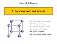
Hartmut S. Leipner: Structure of imperfect materials<br />
2. <strong>Epitaxy</strong> <strong>and</strong> <strong>interface</strong> <strong>defects</strong><br />
2.1 Basic models of epitaxy<br />
2.2 Heteroepitaxy<br />
2.3 Formation of misfit dislocations<br />
2.4 The critical thickness<br />
2.5 Sources of misfit dislocations<br />
2.6 Configuration of misfit dislocations
2.1 Basic models of epitaxy<br />
Growth of a single crystal layer on a single-crystalline substrate<br />
Homoepitaxy: material identical to the substrate<br />
Heteroepitaxy: different material<br />
Why epitaxy?<br />
➢ No bulk material available<br />
➢ Layers with special properties<br />
➢ Only high-quality layers are required (semiconductor technology)<br />
hsl 2007 – Structure of imperfect materials – <strong>Epitaxy</strong> <strong>and</strong> <strong>interface</strong> <strong>defects</strong><br />
2
hsl 2007 – Structure of imperfect materials – <strong>Epitaxy</strong> <strong>and</strong> <strong>interface</strong> <strong>defects</strong><br />
Lattice constants<br />
B<strong>and</strong>gap energy versus lattice constant for a range of elemental <strong>and</strong> compound semiconductors<br />
3
Basic models of homoepitaxy<br />
Energetic considerations:<br />
γ e + γ i ≤ γ s<br />
> γ s<br />
hsl 2007 – Structure of imperfect materials – <strong>Epitaxy</strong> <strong>and</strong> <strong>interface</strong> <strong>defects</strong><br />
γ e<br />
γ i<br />
γ s<br />
Layer-by-layer growth<br />
(Frank–van der Merwe)<br />
2D growth + coalescence<br />
(Volmer–Weber)<br />
4
hsl 2007 – Structure of imperfect materials – <strong>Epitaxy</strong> <strong>and</strong> <strong>interface</strong> <strong>defects</strong><br />
Kinetics of layer growth<br />
Nucleation mechanism Surface morphology<br />
Homogeneous nucleation<br />
(high supersaturation, non-continuous growth)<br />
Heterogeneous nucleation at suitable <strong>defects</strong> – steps<br />
(low supersaturation, continuous growth)<br />
Bundling of steps, wavy surface<br />
(topologically unstable)<br />
Step of monoatomic height in equal<br />
distances (topologically stable)<br />
5
hsl 2007 – Structure of imperfect materials – <strong>Epitaxy</strong> <strong>and</strong> <strong>interface</strong> <strong>defects</strong><br />
Surface steps<br />
Scanning tunneling microscopy of<br />
surface steps on (111) Si.<br />
U = 2.2 V, I = 0.8 nA, 95 × 95 nm.<br />
[Kraus:2001]<br />
6
hsl 2007 – Structure of imperfect materials – <strong>Epitaxy</strong> <strong>and</strong> <strong>interface</strong> <strong>defects</strong><br />
2.2 Heteroepitaxy<br />
Lattice misfit<br />
h a e , E f<br />
Strain energy (per unit thickness h)<br />
a s<br />
γ e<br />
γ i<br />
γ s<br />
7
hsl 2007 – Structure of imperfect materials – <strong>Epitaxy</strong> <strong>and</strong> <strong>interface</strong> <strong>defects</strong><br />
Pseudomorphic growth<br />
Energetic considerations:<br />
γ e + γ i + E f h ≤ γ s<br />
Further growth:<br />
a) Elastic relaxation<br />
b) Plastic relaxation<br />
(E f h increases)<br />
> γ s<br />
Growth of closed layers<br />
(Frank–van der Merwe)<br />
▼<br />
a) 2D growth + coalescence<br />
(Volmer–Weber)<br />
b) Isl<strong>and</strong> growth on top of a wetting layer<br />
(Stranski–Krastanov)<br />
8
Stranski–Krastanov growth<br />
hsl 2007 – Structure of imperfect materials – <strong>Epitaxy</strong> <strong>and</strong> <strong>interface</strong> <strong>defects</strong><br />
Stranski–Krastanov growth of SiGe on (001) Si.<br />
Liquid phase epitaxy. Cross-section TEM image.<br />
[Albrecht, Strunk: 1999]<br />
SiGe<br />
Si<br />
9
hsl 2007 – Structure of imperfect materials – <strong>Epitaxy</strong> <strong>and</strong> <strong>interface</strong> <strong>defects</strong><br />
<strong>Epitaxy</strong> modes<br />
(a) (b) (c)<br />
Growth temperature (°C)<br />
Epitaxial nucleation modes in heteroepitaxy:<br />
a) layer-by-layer, b) Stranski–Krastanov, <strong>and</strong> c) clustered.<br />
Clustered growth<br />
Planar growth<br />
Germanium fraction x<br />
Measurements of clustered vs. layerby-layer<br />
growth in the Si 1 − x Ge x /Si<br />
(001) system for molecular beam<br />
epitaxy.<br />
[Bean et al. 1984]<br />
10
hsl 2007 – Structure of imperfect materials – <strong>Epitaxy</strong> <strong>and</strong> <strong>interface</strong> <strong>defects</strong><br />
Isl<strong>and</strong>s<br />
Scanning tunneling microscopy<br />
of CoO isl<strong>and</strong>s on a Ag substrate.<br />
The diameter of the isl<strong>and</strong><br />
amounts to about 6 – 8 nm. The<br />
layer thickness corresponds to 1,<br />
2, <strong>and</strong> 3 monolayers. Single<br />
atoms in the CoO can be<br />
resolved.<br />
[Widdra 2004]<br />
11
High<br />
growth velocity<br />
Elastic relaxation during isl<strong>and</strong> growth<br />
hsl 2007 – Structure of imperfect materials – <strong>Epitaxy</strong> <strong>and</strong> <strong>interface</strong> <strong>defects</strong><br />
Elastic relaxation<br />
No<br />
growth<br />
Ripples = sinusoidal undulations<br />
Strain<br />
relaxation<br />
High Low<br />
growth velocity<br />
Strain<br />
enhancement<br />
12
hsl 2007 – Structure of imperfect materials – <strong>Epitaxy</strong> <strong>and</strong> <strong>interface</strong> <strong>defects</strong><br />
Ripples<br />
Ripples in Si 0.97 Ge 0.03 on (001) Si. Liquid phase epitaxy.<br />
Light microscopy, Normarski differential interference contrast.<br />
Ripple amplitude 5.4 nm, layer thickness 150 nm, wavelength 11.7 µm.<br />
[Albrecht, Strunk: 1999]<br />
[010]<br />
[100]<br />
100 µm<br />
13
2.3 Formation of misfit dislocations<br />
Pseudomorphic layer<br />
Misfit stress<br />
Thermally unstable against<br />
plastic/diffusive relaxation<br />
hsl 2007 – Structure of imperfect materials – <strong>Epitaxy</strong> <strong>and</strong> <strong>interface</strong> <strong>defects</strong><br />
Relaxed layer<br />
Almost no elastic stress<br />
Rather stable<br />
Presence of lattice <strong>defects</strong><br />
affects processing<br />
Recombination activity<br />
of <strong>defects</strong><br />
14
Modeling of misfit dislocations<br />
What has to be considered?<br />
1. Generation of dislocations<br />
2. Dislocation motion<br />
3. Dislocation multiplication <strong>and</strong> interaction<br />
Conditions<br />
1. Crystallography of the real system – combination of different lattice types<br />
2. Slip geometry<br />
3. Population of intrinsic <strong>defects</strong><br />
Consequence<br />
Restriction on simple systems<br />
hsl 2007 – Structure of imperfect materials – <strong>Epitaxy</strong> <strong>and</strong> <strong>interface</strong> <strong>defects</strong><br />
15
2.4 The concept of critical thickness<br />
h crit thickness at which the self-energy of dislocation is equal to the strain energy<br />
Below h crit , formation of dislocations energetically unfavorable<br />
Frank–van der Merwe: calculation of density of <strong>interface</strong> dislocation from<br />
mathematical analysis of interfacial energy<br />
Matthews–Blakeslee: consideration of the stress on pre-existing, threading<br />
dislocations<br />
Dodson–Tsao: strain relaxation rates are kinetically limited, i. e. dislocation<br />
nucleation <strong>and</strong> growth rates have to be considered<br />
hsl 2007 – Structure of imperfect materials – <strong>Epitaxy</strong> <strong>and</strong> <strong>interface</strong> <strong>defects</strong><br />
16
The Matthews–Blakeslee model<br />
Above the critical thickness, there is a driving force of dislocation motion in the<br />
<strong>interface</strong> due to the lattice mismatch.<br />
For h = h crit , σ t = σ f<br />
(σ t restoring stress due to the line tension of the dislocation, σ f stress due to the lattice<br />
mismatch)<br />
h < h h h = hh h > h > h crit crit crit<br />
crit crit<br />
hsl 2007 – Structure of imperfect materials – <strong>Epitaxy</strong> <strong>and</strong> <strong>interface</strong> <strong>defects</strong><br />
σ t<br />
σ f<br />
17
Measurement of critical thickness<br />
Critical thickness (Å)<br />
Measurement of critical thickness in the Si 1 − x Ge x /Si (001) system<br />
for different growth temperatures vs. the prediction of the Matthews–Blakeslee model<br />
[Hull:94]<br />
hsl 2007 – Structure of imperfect materials – <strong>Epitaxy</strong> <strong>and</strong> <strong>interface</strong> <strong>defects</strong><br />
Germanium fraction x<br />
Theory<br />
550 °C<br />
750 °C<br />
900 °C<br />
18
hsl 2007 – Structure of imperfect materials – <strong>Epitaxy</strong> <strong>and</strong> <strong>interface</strong> <strong>defects</strong><br />
The Dodson–Tsao model<br />
Relaxation of the epitaxial layer is controlled by thermal activation of dislocation<br />
glide processes<br />
Dislocation velocity (analogous bulk material)<br />
(σ eff effective driving stress in MPa, Q activation energy, υ 0 prefactor)<br />
Four stages of strain relaxation in the Dodson–Tsao model<br />
Residual strain<br />
I II III IV<br />
h crit<br />
Layer thickness<br />
19
Intensity (counts)<br />
4000<br />
3000<br />
2000<br />
1000<br />
0<br />
Anisotropic relaxation<br />
in compound semiconductors<br />
PL 1.6 K<br />
d = 495 nm<br />
2 LOY<br />
1 LOY<br />
Matrix luminescence<br />
2.50 2.55 2.60 2.65 2.70 2.75 2.80<br />
Photon energy (eV)<br />
Cathodoluminescence investigation of plastic relaxation in ZnSe/GaAs(001) heterostructures<br />
[Hilpert:2001]<br />
hsl 2007 – Structure of imperfect materials – <strong>Epitaxy</strong> <strong>and</strong> <strong>interface</strong> <strong>defects</strong><br />
Y<br />
Defect emission<br />
(D 0,X)<br />
h = 165 nm h = 495 nm h = 4200 nm<br />
FX<br />
h = 105 nm<br />
100 µm<br />
20
(a)<br />
(b)<br />
2.5 Sources of misfit dislocations<br />
h > h crit<br />
h > h crit<br />
hsl 2007 – Structure of imperfect materials – <strong>Epitaxy</strong> <strong>and</strong> <strong>interface</strong> <strong>defects</strong><br />
Multiplication mechanisms arising<br />
from dislocation pinning or<br />
interaction<br />
Heterogeneous nucleation at<br />
specific local stress concentrations,<br />
e. g. growth artifacts or substrate<br />
<strong>defects</strong><br />
Homogeneous (spontaneous)<br />
nucleation of dislocation loops<br />
Generation of misfit dislocations from<br />
different sources:<br />
a) the pre-existing threading dislocation<br />
model <strong>and</strong> b) the half-loop generation<br />
from the free surface.<br />
[Zou:01] 21
TEM weak-beam image showing the<br />
generation of a misfit dislocation bc<br />
from a threading dislocation ab. The<br />
short segment cd corresponds to the<br />
threading dislocation in the layer.<br />
InGaAs/GaAs single heterostructure.<br />
hsl 2007 – Structure of imperfect materials – <strong>Epitaxy</strong> <strong>and</strong> <strong>interface</strong> <strong>defects</strong><br />
TEM examples<br />
200 nm 1 µm<br />
TEM weak-beam image of the generation<br />
of misfit dislocations at an<br />
inhomogeneous source. InGaAs/GaAs<br />
single heterostructure.<br />
[Zou 2001]<br />
22
Compilation of Vdovin 1999<br />
hsl 2007 – Structure of imperfect materials – <strong>Epitaxy</strong> <strong>and</strong> <strong>interface</strong> <strong>defects</strong><br />
Generation mechanisms<br />
Dislocation behavior Mechanism Author<br />
Bending [Matthews 1966]<br />
Surface generation [Matthews et al. 1970]<br />
Interface generation [Perovic, Houghton 1995]<br />
Interface precipitation [Perovic et al. 1989,<br />
Fitzgerald et al. 1989,<br />
Eaglesham et al. 1989]<br />
23
2.6 Configurations of misfit dislocations<br />
(a) (b)<br />
TEM images from an (001) In 0.1 Ga 0.9 As single heterostructure on (001) GaAs.<br />
a) Layer thickness of 100 nm, b) 200 nm.<br />
[Zou 2001]<br />
hsl 2007 – Structure of imperfect materials – <strong>Epitaxy</strong> <strong>and</strong> <strong>interface</strong> <strong>defects</strong><br />
0.5 µm<br />
24
Alignment of misfit dislocations<br />
Misfit dislocations in (001) ZnSe/GaAs. MBE growth, layer thickness 495 nm.<br />
TEM bright field image.<br />
hsl 2007 – Structure of imperfect materials – <strong>Epitaxy</strong> <strong>and</strong> <strong>interface</strong> <strong>defects</strong><br />
25
Dissociated misfit dislocations<br />
hsl 2007 – Structure of imperfect materials – <strong>Epitaxy</strong> <strong>and</strong> <strong>interface</strong> <strong>defects</strong><br />
Possible configuration of misfit dislocations<br />
[Zou:01] 26
Configuration of a dissociated misfit<br />
dislocation in a heterostructure<br />
hsl 2007 – Structure of imperfect materials – <strong>Epitaxy</strong> <strong>and</strong> <strong>interface</strong> <strong>defects</strong><br />
5 nm<br />
A high-resolution TEM image of a cross-section sample of a InGaAs<br />
heterostructure showing a dissociated 60° misfit dislocation. The 90°<br />
partial is near the strained <strong>interface</strong>, while the 30° is in the substrate.<br />
[Zou 2001]<br />
27
Stacking faults in the epitaxial layer<br />
1 µm<br />
Stacking faults <strong>and</strong> threading dislocations in heteroepitaxial<br />
(111)CdTe/(001)GaAs. TEM bright field image, g diffraction<br />
vector.<br />
hsl 2007 – Structure of imperfect materials – <strong>Epitaxy</strong> <strong>and</strong> <strong>interface</strong> <strong>defects</strong><br />
g<br />
28
hsl 2007 – Structure of imperfect materials – <strong>Epitaxy</strong> <strong>and</strong> <strong>interface</strong> <strong>defects</strong><br />
Defects in CdTe/GaAs<br />
Stacking fault tetrahedra, misfit <strong>and</strong><br />
threading dislocations in<br />
heteroepitaxial (111)CdTe/(001)GaAs.<br />
Plane view transmission electron<br />
microscopy. The cross section of the<br />
TEM foil is shown below.<br />
29
hsl 2007 – Structure of imperfect materials – <strong>Epitaxy</strong> <strong>and</strong> <strong>interface</strong> <strong>defects</strong><br />
References<br />
H. Bethge, J. Heydenreich: Electron microscopy in solid state physics.<br />
Amsterdam: Elsevier 1987.<br />
A. Kraus: Präparation und Charakterisierung von Nanostrukturen mittels<br />
Rastertunnelmikroskopie auf Si(111). Martin-Luther-Universität Halle 2002<br />
H. P. Strunk et al. phys. stat. sol. (a) 171 (1999) 215.<br />
W. Widdra: Sci. hal. 2 (2004) 31.<br />
R. Hull, J. Bean: MRS Bulletin (1994) 32.<br />
U. Hilpert: Defektinduzierte optische und elektronische Eigenschaften von II–VI<br />
Halbleiterheterostrukturen. Martin-Luther-Universität Halle 2001.<br />
J. Zou, D. J. H. Cockayne in: Transmission electron microscopy investigations of misfit<br />
dislocations in lattice-mismatched semiconductor heterostructures. Ed. X.-F. Zhang, Z.<br />
Zhang. Berlin: Springer 2001, p. 247.<br />
V. I. Vdovin: phys. stat. sol. (a) 171 (1999) 215.<br />
X