Epitaxy and interface defects
Epitaxy and interface defects
Epitaxy and interface defects
SHOW LESS

You also want an ePaper? Increase the reach of your titles
YUMPU automatically turns print PDFs into web optimized ePapers that Google loves.
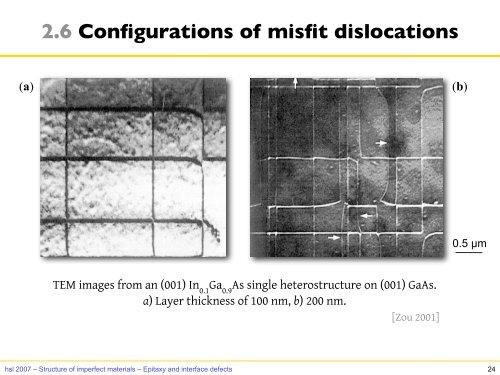
2.6 Configurations of misfit dislocations<br />
(a) (b)<br />
TEM images from an (001) In 0.1 Ga 0.9 As single heterostructure on (001) GaAs.<br />
a) Layer thickness of 100 nm, b) 200 nm.<br />
[Zou 2001]<br />
hsl 2007 – Structure of imperfect materials – <strong>Epitaxy</strong> <strong>and</strong> <strong>interface</strong> <strong>defects</strong><br />
0.5 µm<br />
24