Epitaxy and interface defects
Epitaxy and interface defects
Epitaxy and interface defects

Create successful ePaper yourself
Turn your PDF publications into a flip-book with our unique Google optimized e-Paper software.
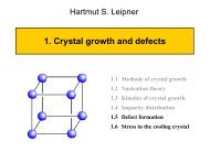
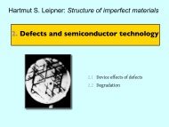
Hartmut S. Leipner: Structure of imperfect materials<br />
2. <strong>Epitaxy</strong> <strong>and</strong> <strong>interface</strong> <strong>defects</strong><br />
2.1 Basic models of epitaxy<br />
2.2 Heteroepitaxy<br />
2.3 Formation of misfit dislocations<br />
2.4 The critical thickness<br />
2.5 Sources of misfit dislocations<br />
2.6 Configuration of misfit dislocations
2.1 Basic models of epitaxy<br />
Growth of a single crystal layer on a single-crystalline substrate<br />
Homoepitaxy: material identical to the substrate<br />
Heteroepitaxy: different material<br />
Why epitaxy?<br />
➢ No bulk material available<br />
➢ Layers with special properties<br />
➢ Only high-quality layers are required (semiconductor technology)<br />
hsl 2007 – Structure of imperfect materials – <strong>Epitaxy</strong> <strong>and</strong> <strong>interface</strong> <strong>defects</strong><br />
2
hsl 2007 – Structure of imperfect materials – <strong>Epitaxy</strong> <strong>and</strong> <strong>interface</strong> <strong>defects</strong><br />
Lattice constants<br />
B<strong>and</strong>gap energy versus lattice constant for a range of elemental <strong>and</strong> compound semiconductors<br />
3
Basic models of homoepitaxy<br />
Energetic considerations:<br />
γ e + γ i ≤ γ s<br />
> γ s<br />
hsl 2007 – Structure of imperfect materials – <strong>Epitaxy</strong> <strong>and</strong> <strong>interface</strong> <strong>defects</strong><br />
γ e<br />
γ i<br />
γ s<br />
Layer-by-layer growth<br />
(Frank–van der Merwe)<br />
2D growth + coalescence<br />
(Volmer–Weber)<br />
4
hsl 2007 – Structure of imperfect materials – <strong>Epitaxy</strong> <strong>and</strong> <strong>interface</strong> <strong>defects</strong><br />
Kinetics of layer growth<br />
Nucleation mechanism Surface morphology<br />
Homogeneous nucleation<br />
(high supersaturation, non-continuous growth)<br />
Heterogeneous nucleation at suitable <strong>defects</strong> – steps<br />
(low supersaturation, continuous growth)<br />
Bundling of steps, wavy surface<br />
(topologically unstable)<br />
Step of monoatomic height in equal<br />
distances (topologically stable)<br />
5
hsl 2007 – Structure of imperfect materials – <strong>Epitaxy</strong> <strong>and</strong> <strong>interface</strong> <strong>defects</strong><br />
Surface steps<br />
Scanning tunneling microscopy of<br />
surface steps on (111) Si.<br />
U = 2.2 V, I = 0.8 nA, 95 × 95 nm.<br />
[Kraus:2001]<br />
6
hsl 2007 – Structure of imperfect materials – <strong>Epitaxy</strong> <strong>and</strong> <strong>interface</strong> <strong>defects</strong><br />
2.2 Heteroepitaxy<br />
Lattice misfit<br />
h a e , E f<br />
Strain energy (per unit thickness h)<br />
a s<br />
γ e<br />
γ i<br />
γ s<br />
7
hsl 2007 – Structure of imperfect materials – <strong>Epitaxy</strong> <strong>and</strong> <strong>interface</strong> <strong>defects</strong><br />
Pseudomorphic growth<br />
Energetic considerations:<br />
γ e + γ i + E f h ≤ γ s<br />
Further growth:<br />
a) Elastic relaxation<br />
b) Plastic relaxation<br />
(E f h increases)<br />
> γ s<br />
Growth of closed layers<br />
(Frank–van der Merwe)<br />
▼<br />
a) 2D growth + coalescence<br />
(Volmer–Weber)<br />
b) Isl<strong>and</strong> growth on top of a wetting layer<br />
(Stranski–Krastanov)<br />
8
Stranski–Krastanov growth<br />
hsl 2007 – Structure of imperfect materials – <strong>Epitaxy</strong> <strong>and</strong> <strong>interface</strong> <strong>defects</strong><br />
Stranski–Krastanov growth of SiGe on (001) Si.<br />
Liquid phase epitaxy. Cross-section TEM image.<br />
[Albrecht, Strunk: 1999]<br />
SiGe<br />
Si<br />
9
hsl 2007 – Structure of imperfect materials – <strong>Epitaxy</strong> <strong>and</strong> <strong>interface</strong> <strong>defects</strong><br />
<strong>Epitaxy</strong> modes<br />
(a) (b) (c)<br />
Growth temperature (°C)<br />
Epitaxial nucleation modes in heteroepitaxy:<br />
a) layer-by-layer, b) Stranski–Krastanov, <strong>and</strong> c) clustered.<br />
Clustered growth<br />
Planar growth<br />
Germanium fraction x<br />
Measurements of clustered vs. layerby-layer<br />
growth in the Si 1 − x Ge x /Si<br />
(001) system for molecular beam<br />
epitaxy.<br />
[Bean et al. 1984]<br />
10
hsl 2007 – Structure of imperfect materials – <strong>Epitaxy</strong> <strong>and</strong> <strong>interface</strong> <strong>defects</strong><br />
Isl<strong>and</strong>s<br />
Scanning tunneling microscopy<br />
of CoO isl<strong>and</strong>s on a Ag substrate.<br />
The diameter of the isl<strong>and</strong><br />
amounts to about 6 – 8 nm. The<br />
layer thickness corresponds to 1,<br />
2, <strong>and</strong> 3 monolayers. Single<br />
atoms in the CoO can be<br />
resolved.<br />
[Widdra 2004]<br />
11
High<br />
growth velocity<br />
Elastic relaxation during isl<strong>and</strong> growth<br />
hsl 2007 – Structure of imperfect materials – <strong>Epitaxy</strong> <strong>and</strong> <strong>interface</strong> <strong>defects</strong><br />
Elastic relaxation<br />
No<br />
growth<br />
Ripples = sinusoidal undulations<br />
Strain<br />
relaxation<br />
High Low<br />
growth velocity<br />
Strain<br />
enhancement<br />
12
hsl 2007 – Structure of imperfect materials – <strong>Epitaxy</strong> <strong>and</strong> <strong>interface</strong> <strong>defects</strong><br />
Ripples<br />
Ripples in Si 0.97 Ge 0.03 on (001) Si. Liquid phase epitaxy.<br />
Light microscopy, Normarski differential interference contrast.<br />
Ripple amplitude 5.4 nm, layer thickness 150 nm, wavelength 11.7 µm.<br />
[Albrecht, Strunk: 1999]<br />
[010]<br />
[100]<br />
100 µm<br />
13
2.3 Formation of misfit dislocations<br />
Pseudomorphic layer<br />
Misfit stress<br />
Thermally unstable against<br />
plastic/diffusive relaxation<br />
hsl 2007 – Structure of imperfect materials – <strong>Epitaxy</strong> <strong>and</strong> <strong>interface</strong> <strong>defects</strong><br />
Relaxed layer<br />
Almost no elastic stress<br />
Rather stable<br />
Presence of lattice <strong>defects</strong><br />
affects processing<br />
Recombination activity<br />
of <strong>defects</strong><br />
14
Modeling of misfit dislocations<br />
What has to be considered?<br />
1. Generation of dislocations<br />
2. Dislocation motion<br />
3. Dislocation multiplication <strong>and</strong> interaction<br />
Conditions<br />
1. Crystallography of the real system – combination of different lattice types<br />
2. Slip geometry<br />
3. Population of intrinsic <strong>defects</strong><br />
Consequence<br />
Restriction on simple systems<br />
hsl 2007 – Structure of imperfect materials – <strong>Epitaxy</strong> <strong>and</strong> <strong>interface</strong> <strong>defects</strong><br />
15
2.4 The concept of critical thickness<br />
h crit thickness at which the self-energy of dislocation is equal to the strain energy<br />
Below h crit , formation of dislocations energetically unfavorable<br />
Frank–van der Merwe: calculation of density of <strong>interface</strong> dislocation from<br />
mathematical analysis of interfacial energy<br />
Matthews–Blakeslee: consideration of the stress on pre-existing, threading<br />
dislocations<br />
Dodson–Tsao: strain relaxation rates are kinetically limited, i. e. dislocation<br />
nucleation <strong>and</strong> growth rates have to be considered<br />
hsl 2007 – Structure of imperfect materials – <strong>Epitaxy</strong> <strong>and</strong> <strong>interface</strong> <strong>defects</strong><br />
16
The Matthews–Blakeslee model<br />
Above the critical thickness, there is a driving force of dislocation motion in the<br />
<strong>interface</strong> due to the lattice mismatch.<br />
For h = h crit , σ t = σ f<br />
(σ t restoring stress due to the line tension of the dislocation, σ f stress due to the lattice<br />
mismatch)<br />
h < h h h = hh h > h > h crit crit crit<br />
crit crit<br />
hsl 2007 – Structure of imperfect materials – <strong>Epitaxy</strong> <strong>and</strong> <strong>interface</strong> <strong>defects</strong><br />
σ t<br />
σ f<br />
17
Measurement of critical thickness<br />
Critical thickness (Å)<br />
Measurement of critical thickness in the Si 1 − x Ge x /Si (001) system<br />
for different growth temperatures vs. the prediction of the Matthews–Blakeslee model<br />
[Hull:94]<br />
hsl 2007 – Structure of imperfect materials – <strong>Epitaxy</strong> <strong>and</strong> <strong>interface</strong> <strong>defects</strong><br />
Germanium fraction x<br />
Theory<br />
550 °C<br />
750 °C<br />
900 °C<br />
18
hsl 2007 – Structure of imperfect materials – <strong>Epitaxy</strong> <strong>and</strong> <strong>interface</strong> <strong>defects</strong><br />
The Dodson–Tsao model<br />
Relaxation of the epitaxial layer is controlled by thermal activation of dislocation<br />
glide processes<br />
Dislocation velocity (analogous bulk material)<br />
(σ eff effective driving stress in MPa, Q activation energy, υ 0 prefactor)<br />
Four stages of strain relaxation in the Dodson–Tsao model<br />
Residual strain<br />
I II III IV<br />
h crit<br />
Layer thickness<br />
19
Intensity (counts)<br />
4000<br />
3000<br />
2000<br />
1000<br />
0<br />
Anisotropic relaxation<br />
in compound semiconductors<br />
PL 1.6 K<br />
d = 495 nm<br />
2 LOY<br />
1 LOY<br />
Matrix luminescence<br />
2.50 2.55 2.60 2.65 2.70 2.75 2.80<br />
Photon energy (eV)<br />
Cathodoluminescence investigation of plastic relaxation in ZnSe/GaAs(001) heterostructures<br />
[Hilpert:2001]<br />
hsl 2007 – Structure of imperfect materials – <strong>Epitaxy</strong> <strong>and</strong> <strong>interface</strong> <strong>defects</strong><br />
Y<br />
Defect emission<br />
(D 0,X)<br />
h = 165 nm h = 495 nm h = 4200 nm<br />
FX<br />
h = 105 nm<br />
100 µm<br />
20
(a)<br />
(b)<br />
2.5 Sources of misfit dislocations<br />
h > h crit<br />
h > h crit<br />
hsl 2007 – Structure of imperfect materials – <strong>Epitaxy</strong> <strong>and</strong> <strong>interface</strong> <strong>defects</strong><br />
Multiplication mechanisms arising<br />
from dislocation pinning or<br />
interaction<br />
Heterogeneous nucleation at<br />
specific local stress concentrations,<br />
e. g. growth artifacts or substrate<br />
<strong>defects</strong><br />
Homogeneous (spontaneous)<br />
nucleation of dislocation loops<br />
Generation of misfit dislocations from<br />
different sources:<br />
a) the pre-existing threading dislocation<br />
model <strong>and</strong> b) the half-loop generation<br />
from the free surface.<br />
[Zou:01] 21
TEM weak-beam image showing the<br />
generation of a misfit dislocation bc<br />
from a threading dislocation ab. The<br />
short segment cd corresponds to the<br />
threading dislocation in the layer.<br />
InGaAs/GaAs single heterostructure.<br />
hsl 2007 – Structure of imperfect materials – <strong>Epitaxy</strong> <strong>and</strong> <strong>interface</strong> <strong>defects</strong><br />
TEM examples<br />
200 nm 1 µm<br />
TEM weak-beam image of the generation<br />
of misfit dislocations at an<br />
inhomogeneous source. InGaAs/GaAs<br />
single heterostructure.<br />
[Zou 2001]<br />
22
Compilation of Vdovin 1999<br />
hsl 2007 – Structure of imperfect materials – <strong>Epitaxy</strong> <strong>and</strong> <strong>interface</strong> <strong>defects</strong><br />
Generation mechanisms<br />
Dislocation behavior Mechanism Author<br />
Bending [Matthews 1966]<br />
Surface generation [Matthews et al. 1970]<br />
Interface generation [Perovic, Houghton 1995]<br />
Interface precipitation [Perovic et al. 1989,<br />
Fitzgerald et al. 1989,<br />
Eaglesham et al. 1989]<br />
23
2.6 Configurations of misfit dislocations<br />
(a) (b)<br />
TEM images from an (001) In 0.1 Ga 0.9 As single heterostructure on (001) GaAs.<br />
a) Layer thickness of 100 nm, b) 200 nm.<br />
[Zou 2001]<br />
hsl 2007 – Structure of imperfect materials – <strong>Epitaxy</strong> <strong>and</strong> <strong>interface</strong> <strong>defects</strong><br />
0.5 µm<br />
24
Alignment of misfit dislocations<br />
Misfit dislocations in (001) ZnSe/GaAs. MBE growth, layer thickness 495 nm.<br />
TEM bright field image.<br />
hsl 2007 – Structure of imperfect materials – <strong>Epitaxy</strong> <strong>and</strong> <strong>interface</strong> <strong>defects</strong><br />
25
Dissociated misfit dislocations<br />
hsl 2007 – Structure of imperfect materials – <strong>Epitaxy</strong> <strong>and</strong> <strong>interface</strong> <strong>defects</strong><br />
Possible configuration of misfit dislocations<br />
[Zou:01] 26
Configuration of a dissociated misfit<br />
dislocation in a heterostructure<br />
hsl 2007 – Structure of imperfect materials – <strong>Epitaxy</strong> <strong>and</strong> <strong>interface</strong> <strong>defects</strong><br />
5 nm<br />
A high-resolution TEM image of a cross-section sample of a InGaAs<br />
heterostructure showing a dissociated 60° misfit dislocation. The 90°<br />
partial is near the strained <strong>interface</strong>, while the 30° is in the substrate.<br />
[Zou 2001]<br />
27
Stacking faults in the epitaxial layer<br />
1 µm<br />
Stacking faults <strong>and</strong> threading dislocations in heteroepitaxial<br />
(111)CdTe/(001)GaAs. TEM bright field image, g diffraction<br />
vector.<br />
hsl 2007 – Structure of imperfect materials – <strong>Epitaxy</strong> <strong>and</strong> <strong>interface</strong> <strong>defects</strong><br />
g<br />
28
hsl 2007 – Structure of imperfect materials – <strong>Epitaxy</strong> <strong>and</strong> <strong>interface</strong> <strong>defects</strong><br />
Defects in CdTe/GaAs<br />
Stacking fault tetrahedra, misfit <strong>and</strong><br />
threading dislocations in<br />
heteroepitaxial (111)CdTe/(001)GaAs.<br />
Plane view transmission electron<br />
microscopy. The cross section of the<br />
TEM foil is shown below.<br />
29
hsl 2007 – Structure of imperfect materials – <strong>Epitaxy</strong> <strong>and</strong> <strong>interface</strong> <strong>defects</strong><br />
References<br />
H. Bethge, J. Heydenreich: Electron microscopy in solid state physics.<br />
Amsterdam: Elsevier 1987.<br />
A. Kraus: Präparation und Charakterisierung von Nanostrukturen mittels<br />
Rastertunnelmikroskopie auf Si(111). Martin-Luther-Universität Halle 2002<br />
H. P. Strunk et al. phys. stat. sol. (a) 171 (1999) 215.<br />
W. Widdra: Sci. hal. 2 (2004) 31.<br />
R. Hull, J. Bean: MRS Bulletin (1994) 32.<br />
U. Hilpert: Defektinduzierte optische und elektronische Eigenschaften von II–VI<br />
Halbleiterheterostrukturen. Martin-Luther-Universität Halle 2001.<br />
J. Zou, D. J. H. Cockayne in: Transmission electron microscopy investigations of misfit<br />
dislocations in lattice-mismatched semiconductor heterostructures. Ed. X.-F. Zhang, Z.<br />
Zhang. Berlin: Springer 2001, p. 247.<br />
V. I. Vdovin: phys. stat. sol. (a) 171 (1999) 215.<br />
X