Amateur Radio Report Card
1 - Free and Open Source Software
1 - Free and Open Source Software
- No tags were found...

You also want an ePaper? Increase the reach of your titles
YUMPU automatically turns print PDFs into web optimized ePapers that Google loves.
'7:1<br />
UA.r:.A.7UJI:<br />
Fig. 4<br />
LOAD<br />
SWITCHING<br />
DIOD E<br />
HIGH<br />
IMPEDANCE<br />
TO AC<br />
the "conductive bands" where it can migrate<br />
as an electric current when only a small voltage<br />
is applied across the semiconductor crystal.<br />
Group V impurities prod uce a region of "freeable"<br />
electrons which is commonly called an<br />
"N" region. On the other hand, Group III impurities<br />
in a tetrahedral lattice produce a region<br />
of "electron deficiency" known as a " P"<br />
region. It is possible for a P-region as well as<br />
an N-region to conduct electric current because<br />
both freeable electrons and electron deficiencies<br />
(called "holes") can migrate through<br />
a semiconductor crystal lattice if the proper<br />
impurity density has been established.<br />
A semiconductor diode is manufactured by<br />
forming a junction between a piece of N-type<br />
and P-type semicond uctor crystal material.<br />
Because diode switch circuits, as we will see<br />
later, operate by virtue of changing bias polarity<br />
and voltage across the switching diode, it<br />
might be helpful to quickly examine the electronic<br />
operation of reverse and forward biased<br />
diodes.<br />
Fig. 2 shows a reversed biased diode. The<br />
"holes" in the P-region are attracted by electrostatic<br />
forces toward the negative terminal<br />
of the applied voltage, a direction away from<br />
the P-N junction. At the same time the "free<br />
electrons" in the N-region migrate away from<br />
junction towards the diode electrode<br />
which is connected to the positive battery<br />
terminal. Remembering that the basic units<br />
for voltage ("volts") are joules per elementary<br />
charge, it follows that as the reverse bias voltage<br />
is raised, the electrostatic forces acting on<br />
the carriers (ie. freeable electrons and holes)<br />
increase. Thus as the bias increases, the concentration<br />
of carriers further decreases in the<br />
t<br />
BIAS<br />
AMPL ITUDE<br />
i<br />
~---'"<br />
. , ,<br />
lNSTANTANEOUS VALUES<br />
OF BIAS<br />
regions of the N and P crystals near the p .;-.I<br />
junction. Under normal conditions current cannot<br />
flow through the reverse biased diode because<br />
a "depletion zone" of carriers exists at<br />
the P-N junction and there is no available<br />
mechanism for a transfer of charge. Under abnormal<br />
conditions (for most purposes ), the<br />
reversed biased diode may be made to conduct<br />
by raising the bias voltage to the point<br />
where "break down" occurs in the crystal with<br />
chemical decomposition and the formation of<br />
movable ions.<br />
In a forward biased diode, the situation is<br />
reversed. See Fig. 3. Due to the bias voltage<br />
polarity difference in the forward biased d i<br />
ode, the carriers migrate across the P-N junction<br />
instead of away from it. This permits<br />
current to flow through the diode.<br />
So far, we have looked at forward and reverse<br />
biased diode circuits where the bias<br />
voltage or current has remained constant with<br />
time. In practical diode switching circuits<br />
where ac voltages and currents are being<br />
switched, however, the effective values of<br />
"bias" current and voltage vary with time.<br />
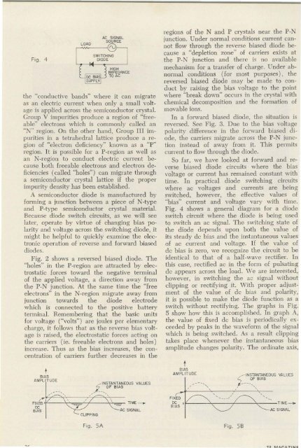
Fig. 4 shows a general diagram for a diode<br />
switch circuit where the diode is being used<br />
to switch an ac signa l. The switching state of<br />
the diode depends upon both the value 01<br />
its steady dc bias and the instantaneous values<br />
of ac current and voltage. If the value of<br />
dc bias is zero, we recognize the circuit to be<br />
identical to that of a half-wave rectifier. In<br />
this case, rectified ac in the form of pulsating<br />
dc appears across the load. We are interested ,<br />
however, in switching the ac signal without<br />
clipping or rectifying it. With proper adjustment<br />
of the value of dc bias and polarity,<br />
it is possible to make the diode function as a<br />
switch without rectifying. The graphs in Fig.<br />
5 show how this is accomplished. In graph A,<br />
the value of fixed de bias is periodicall y exceeded<br />
by peaks in the waveform of the signal<br />
which is being switched. As a result clipping<br />
takes place whenever the instantaneous bias<br />
amplitude changes polarity. The ordinate axis,<br />
t<br />
BIAS<br />
AM PL IT UOE<br />
,<br />
VALUES<br />
OF BIAS<br />
f-INSTANTANEOUS<br />
.<br />
~ - - -<br />
, , '<br />
, ,<br />
-,<br />
....... AC SIGNAL<br />
F;g. 5A F;g. 58