LÜ-LCD-Dispalys_14
LCD-Displays
LCD-Displays

Create successful ePaper yourself
Turn your PDF publications into a flip-book with our unique Google optimized e-Paper software.
TFT TRANSMISSIVE <strong>LCD</strong> MODULES<br />
YTS 570ELAA-01-100T<br />
5.7’’, 320 X 240 DOTS, 1/240 DUTY<br />
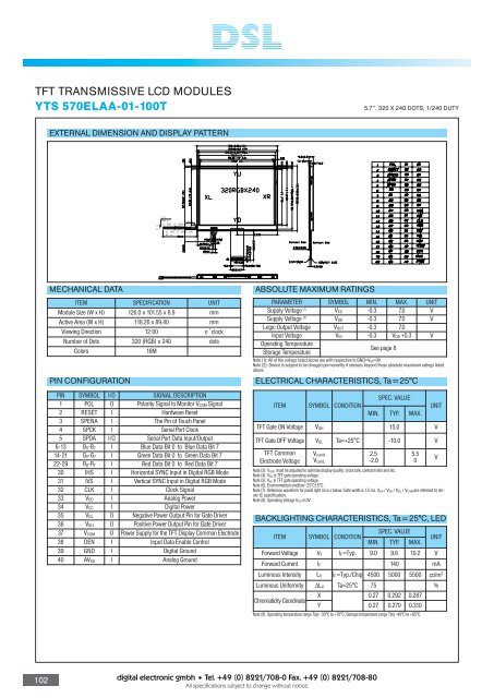
EXTERNAL DIMENSION AND DISPLAY PATTERN<br />
<br />
<br />
<br />
<br />
<br />
<br />
<br />
<br />
MECHANICAL DATA<br />
ITEM SPECIFICATION UNIT<br />
Module Size (W x H) 126.0 x 101.55 x 6.9 mm<br />
Active Area (W x H) 118.26 x 89.40 mm<br />
Viewing Direction 12:00 o´clock<br />
Number of Dots 320 (RGB) x 240 dots<br />
Colors<br />
16M<br />
PIN CONFIGURATION<br />
PIN SYMBOL I/O SIGNAL DESCRIPTION<br />
1 POL O Polarity Signal to Monitor V COM Signal<br />
2 RESET I Hardware Reset<br />
3 SPENA I The Pin of Touch Panel<br />
4 SPCK I Serial Port Clock<br />
5 SPDA I/O Serial Port Data Input/Output<br />
6-13 B 0-B 7 I Blue Data Bit 0 to Blue Data Bit 7<br />
<strong>14</strong>-21 G 0-G 7 I Green Data Bit 0 to Green Data Bit 7<br />
22-29 R 0-R 7 I Red Data Bit 0 to Red Data Bit 7<br />
30 IHS I Horizontal SYNC Input in Digital RGB Mode<br />
31 IVS I Vertical SYNC Input in Digital RGB Mode<br />
32 CLK I Clock Signal<br />
33 V DD I Analog Power<br />
34 V CC I Digital Power<br />
35 V GL O Negative Power Output Pin for Gate Driver<br />
36 V GH O Positive Power Output Pin for Gate Driver<br />
37 V COM O Power Supply for the TFT Display Common Electrode<br />
38 DEN I Input Data Enable Control<br />
39 GND I Digital Ground<br />
40 AV SS I Analog Ground<br />
ABSOLUTE MAXIMUM RATINGS<br />
PARAMETER SYMBOL MIN. MAX. UNIT<br />
Supply Voltage (1) V CC -0.3 7.0 V<br />
Supply Voltage (2) V DD -0.3 7.0 V<br />
Logic Output Voltage V OUT -0.3 7.0<br />
Input Voltage V IN -0.3 V DD +0.3 V<br />
Operating Temperature<br />
Storage Temperature<br />
See page 8<br />
Note (1): All of the voltage listed above are with respective to GND=VSS=0V<br />
Note (2): Device is subjest to be dmaged permanently if stresses beyond those absolute maximum ratings listed<br />
above.<br />
ELECTRICAL CHARACTERISTICS, Ta = 25°C<br />
ITEM<br />
SYMBOL CONDITION<br />
SPEC. VALUE<br />
MIN. TYP. MAX.<br />
TFT Gate ON Voltage V GH 15.0 V<br />
TFT Gate OFF Voltage V GL Ta=+25°C -10.0 V<br />
TFT Common<br />
Electrode Voltage<br />
V comH<br />
V comL<br />
2.5<br />
-2.0<br />
UNIT<br />
5.5<br />
0<br />
V<br />
Note (3): V com must be adjusted to optimize display quality: cross talk, contrast ratio and etc.<br />
Note (4): VGH is TFT gate operating voltage.<br />
Note (5): VGL is TFT gate operating voltage.<br />
Note (6): Environmental condition: 25°C±5°C.<br />
Note (7): Reference waveform for panel light on is s below: Gate width is 1.5 ms. VGH / VDH / VGL / VCOM are referred to driver<br />
IC specification.<br />
Note (8): Operating Voltage VCC=5.0V<br />
BACKLIGHTING CHARACTERISTICS, Ta = 25°C, LED<br />
ITEM SYMBOL CONDITION<br />
SPEC. VALUE<br />
MIN. TYP. MAX.<br />
UNIT<br />
Forward Voltage V f I F =Typ. 9.0 9.6 10.2 V<br />
Forward Current I F <strong>14</strong>0 mA<br />
Luminous Intensity L V I F =Typ./Chip 4500 5000 5500 cd/m 2<br />
Luminous Uniformity DL V Ta=25°C 75 %<br />
Chromaticity Coordinate<br />
X 0.27 0.292 0.287<br />
Y 0.27 0.270 0.310<br />
Note (9): Operating temperature range Topr -30°C to +70°C; Storage temperature range Tsty -40°C to +85°C.<br />
102<br />
digital electronic gmbh Tel. +49 (0) 8221/708-0 Fax. +49 (0) 8221/708-80<br />
All specifications subject to change without notice.