LÜ-LCD-Dispalys_14
LCD-Displays
LCD-Displays

You also want an ePaper? Increase the reach of your titles
YUMPU automatically turns print PDFs into web optimized ePapers that Google loves.
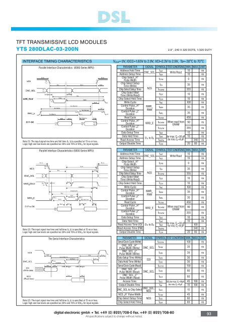
TFT TRANSMISSIVE <strong>LCD</strong> MODULES<br />
YTS 280DLAC-03-200N<br />
2.8’’, 240 X 320 DOTS, 1/320 DUTY<br />
INTERFACE TIMING CHARACTERISTICS V SSA = 0V, IOCC=1.65V to 2.9V, VCI=2.3V to 2.9V, Ta=-30°C to 70°C<br />
Parallel Interface Characteristics (8080 Series MPU)<br />
Note (1): The input signal rise time and fall time (t r, t f) is specified at 15 ns or less.<br />
Logic high and low levels are specified as 30% and 70% of IOV CC for input signals.<br />
Parallel Interface Characteristics (6800 Series MPU)<br />
Note (2): The input signal rise time and fall time (t r, t f) is specified at 15 ns or less.<br />
Logic high and low levels are specified as 30% and 70% of IOV CC for input signals.<br />
PARAMETER SIGNAL SYMBOL TEST CONDITIONS MIN. MAX. UNIT<br />
Address Hold Time<br />
t AHT<br />
10 ns<br />
DNC_SCL Write/Read<br />
Address Setup Time t AST 10 ns<br />
Chip Select „H“<br />
Pulse Width<br />
t CHW 0 ns<br />
Chip Select Setup<br />
Time (Write)<br />
t CS 35 ns<br />
Chip Select Setup Time NCS t RCSFM 355 ns<br />
Chip Select Wait<br />
Time (Write/Read)<br />
t CSF 10 ns<br />
Chip Select Hold Time t CSH 10 ns<br />
Write Cycle<br />
t WC 100 ns<br />
Control Pulse „H“ NWR_<br />
Duration<br />
t WRH 35 ns<br />
RNW<br />
Control Pulse „L“<br />
Duration<br />
t WRL 35 ns<br />
Read Cycle<br />
t RCFM<br />
450 ns<br />
Control Pulse „H“<br />
NRD_E<br />
When read from<br />
Duration<br />
t RDHFM 90 ns<br />
GRAM<br />
Control Pulse „L“<br />
Duration<br />
t RDLFM 355 ns<br />
t Data Setup Time<br />
15 ns<br />
DST<br />
Data Hold Time t<br />
D 17 to D DHT for max. C<br />
0<br />
L=30 pF 10 ns<br />
Read Access Time t RATFM for min. C L=8 pF 340 ns<br />
Output Disable Time t ODH 20 80 ns<br />
PARAMETER SIGNAL SYMBOL TEST CONDITIONS MIN. MAX. UNIT<br />
Address Hold Time<br />
t AHT<br />
10 ns<br />
DNC_SCL Write/Read<br />
Address Setup Time t AST 10 ns<br />
Chip Select „H“<br />
Pulse Width<br />
t CHW 0 ns<br />
Chip Select Setup<br />
Time (Write)<br />
t CS 35 ns<br />
Chip Select Setup Time NCS t RCSFM 355 ns<br />
Chip Select Wait<br />
Time (Write/Read)<br />
t CSF 10 ns<br />
Chip Select Hold Time t CSH 10 ns<br />
Write Cycle<br />
t WC 100 ns<br />
Control Pulse „H“ NWR_<br />
Duration<br />
t WRH 35 ns<br />
RNW<br />
Control Pulse „L“<br />
Duration<br />
t WRL 35 ns<br />
Read Cycle<br />
t RCFM<br />
450 ns<br />
Control Pulse „H“<br />
NRD_E<br />
When read from<br />
Duration<br />
t RDHFM 90 ns<br />
GRAM<br />
Control Pulse „L“<br />
Duration<br />
t RDLFM 355 ns<br />
t Data Setup Time<br />
10 ns<br />
DST<br />
Data Hold Time t DHT 10 ns<br />
Read Access Time (ID) D 17 to D<br />
for max. C<br />
0 t L=30 pF<br />
RAT<br />
for min. C L=8 pF<br />
100<br />
Read Access Time (FM) t RATFM 340 ns<br />
Output Disable Time t ODH 20 80 ns<br />
The Serial Interface Characteristics PARAMETER SIGNAL SYMBOL TEST CONDITIONS MIN. MAX. UNIT<br />
Senal Clock Cycle (Write)<br />
t SCYCW 100 ns<br />
DNC_SCL „H“<br />
Pulse Width (Write) DNC_SCL t SHW 35 ns<br />
DNC_SCL „L“<br />
Pulse Width (Write)<br />
t SLW 35 ns<br />
Data Setup Time (Write)<br />
t SDS 30 ns<br />
SDI<br />
Data Hold Time (Write) t SDH 30 ns<br />
Senal Clock Cycle (Read)<br />
t SCYCR 150 ns<br />
DNC_SCL „H“<br />
Pulse Width (Read) DNC_SCL t SHR 60 ns<br />
DNC_SCL „L“<br />
Pulse Width (Read)<br />
t SLR 60 ns<br />
Access Time t ACC SD0 for max. C L=30pF, 45 100 ns<br />
Output Disable Time t OH for min. C L=8 pF 15 100 ns<br />
DNC_SCL to Chip Select DNC_SCL,<br />
NCS<br />
t SCC 15 ns<br />
NCS „H“ Pulse Width<br />
t CHW 45 ns<br />
Chip Select Setup Time NCS t CSS 60 ns<br />
Note (2): The input signal rise time and fall time (t r, t f) is specified at 15 ns or less.<br />
Logic high and low levels are specified as 30% and 70% of IOV CC for input signals.<br />
Chip Select Hold Time t CSH 65 ns<br />
digital electronic gmbh Tel. +49 (0) 8221/708-0 Fax. +49 (0) 8221/708-80<br />
All specifications subject to change without notice.<br />
93