LÜ-LCD-Dispalys_14
LCD-Displays
LCD-Displays

You also want an ePaper? Increase the reach of your titles
YUMPU automatically turns print PDFs into web optimized ePapers that Google loves.
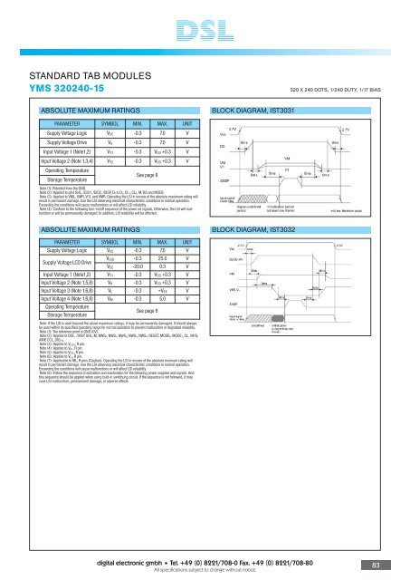
STANDARD TAB MODULES<br />
YMS 320240-15<br />
320 X 240 DOTS, 1/240 DUTY, 1/17 BIAS<br />
ABSOLUTE MAXIMUM RATINGS<br />
BLOCK DIAGRAM, IST3031<br />
PARAMETER SYMBOL MIN. MAX. UNIT<br />
Supply Voltage Logic V CC -0.3 7.0 V<br />
Supply Voltage Drive V 0 -0.3 7.0 V<br />
Input Voltage 1 (Note1,2) V T1 -0.3 V DD +0.3 V<br />
Input Voltage 2 (Note 1,3,4) V T2 -0.3 V DD +0.3 V<br />
Operating Temperature<br />
Storage Temperature<br />
See page 8<br />
Note (1): Potential from the GND.<br />
Note (2): Applied to pins SHL, /EIO1, /EIO2, /DISP, D0 to D7, CL1, CL2, M, BS and MODE.<br />
Note (3): Applied to VML, VMR, V1L and VMR. Operating the LSI in excess of the absolute maximum rating will<br />
result in permanent damage. Use the LSI observing electrical characteristic conditions in normal operation.<br />
Exceeding the conditions will cause malfunctions or will affect LSI reliability.<br />
Note (4): Conform to the following turn-on/off sequence of the power nd signals. Otherwise, the LSI will malfunction<br />
or will be permanently damaged. In addition, LSI reliability will be affected.<br />
ABSOLUTE MAXIMUM RATINGS<br />
BLOCK DIAGRAM, IST3032<br />
PARAMETER SYMBOL MIN. MAX. UNIT<br />
Supply Voltage Logic V CC -0.3 7.0 V<br />
Supply Voltage <strong>LCD</strong> Drive<br />
V <strong>LCD</strong> -0.3 25.0 V<br />
V EE -20.0 0.3 V<br />
Input Voltage 1 (Note1,2) V T1 -0.3 V DD +0.3 V<br />
Input Voltage 2 (Note 1,5,8) V H -0.3 V DD +0.3 V<br />
Input Voltage 3 (Note 1,6,8) V L -0.3 +V EE V<br />
Input Voltage 4 (Note 1,6,8) V M -0.3 5.0 V<br />
Operating Temperature<br />
Storage Temperature<br />
See page 8<br />
Note: If the LSI is used beyond the above maximum ratings, it may be permanently damaged. It should always<br />
be used within its specified operating range for normal operation to prevent malfunction or degraded reliability.<br />
Note (1): The reference point is GND (0V).<br />
Note (2): Applies to DIO1, /DISP, SHL, M, NWS0, NWS1, NWS2, NWS3, NWS4, RESET, MODE0, MODE1, CL, /M/S,<br />
AMP, CCL, DIO2*3.<br />
Note (3): Applies to V<strong>LCD</strong>L, R pin.<br />
Note (4): Applies to VHL, R pin.<br />
Note (5): Applies to VEEL, R pin.<br />
Note (6): Applies to VLL, R pin.<br />
Note (7): Applicable to ML, R pins (Caution). Operating the LSI in excess of the absolute mximum rating will<br />
result in permanent damage. Use the LSI observing electrical characteristic conditions in normal operation.<br />
Exceeding the conditions will cause malfunctions or will affect LSI reliability.<br />
Note (8): Follow the sequence of activation and inactivation for the following power supplies and signals. And<br />
this sequence should be applied when using built-in switchung circuit. If the sequence is not followed, it may<br />
cuse LSI malfunction, permamnent damage, or adverse effects.<br />
digital electronic gmbh Tel. +49 (0) 8221/708-0 Fax. +49 (0) 8221/708-80<br />
All specifications subject to change without notice.<br />
83