LU-QORF_6-2016

Create successful ePaper yourself
Turn your PDF publications into a flip-book with our unique Google optimized e-Paper software.
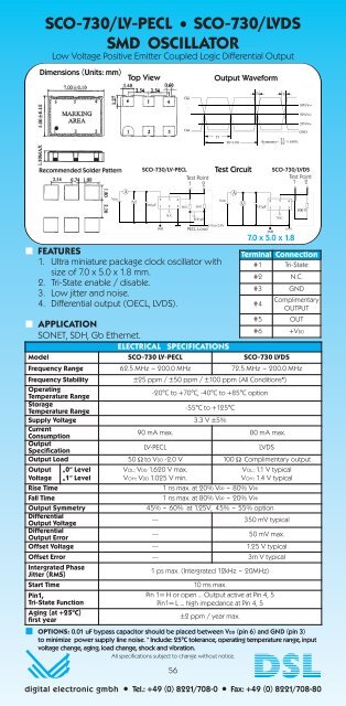
SCO-730/LV-PECL • SCO-730/LVDS<br />
SMD OSCILLATOR<br />
Low Voltage Positive Emitter Coupled Logic Differential Output<br />
Dimensions (Units: mm)<br />
Top View<br />
Output Waveform<br />
Recommended Solder Pattern<br />
SCO-730/LV-PECL Test Circuit SCO-730/LVDS<br />
Test Point<br />
Test Point<br />
1 2 1 2<br />
FEATURES<br />
1. Ultra miniature package clock oscillator with<br />
size of 7.0 x 5.0 x 1.8 mm.<br />
2. Tri-State enable / disable.<br />
3. Low jitter and noise.<br />
4. Differential output (OECL, LVDS).<br />
OPTIONS: 0.01 uF bypass capacitor should be placed between VDD (pin 6) and GND (pin 3)<br />
to minimize power supply line noise. * Include: 25°C tolerance, operating temperature range, input<br />
voltage change, aging, load change, shock and vibration.<br />
All specifications subject to change without notice.<br />
56<br />
18.4 x 9.3 x 19.7<br />
Terminal Connection<br />
#1 Tri-State<br />
#2 N.C.<br />
#3 GND<br />
#4<br />
Complimentary<br />
OUTPUT<br />
APPLICATION<br />
SONET, SDH, Gb Ethernet.<br />
#5<br />
#6<br />
OUT<br />
+VDD<br />
ELECTRICAL SPECIFICATIONS<br />
Model SCO-730 LV-PECL SCO-730 LVDS<br />
Frequency Range 62.5 MHz ~ 200.0 MHz 72.5 MHz ~ 200.0 MHz<br />
Frequency Stability<br />
±25 ppm / ±50 ppm / ±100 ppm (All Conditions*)<br />
Operating<br />
Temperature Range<br />
-20°C to +70°C, -40°C to +85°C option<br />
Storage<br />
Temperature Range<br />
-55°C to +125°C<br />
Supply Voltage 3.3 V ±5%<br />
Current<br />
Consumption<br />
90 mA max. 80 mA max.<br />
Output<br />
Specification<br />
LV-PECL<br />
LVDS<br />
Output Load 50 W to VDD -2.0 V 100 W Complimentary output<br />
Output<br />
Voltage<br />
„0“ Level<br />
„1“ Level<br />
VOL: VDD 1.620 V max.<br />
VOH: VDD 1.025 V min.<br />
VOL: 1.1 V typical<br />
VOH: 1.4 V typical<br />
Rise Time<br />
1 ns max. at 20% VPP ~ 80% VPP<br />
Fall Time<br />
1 ns max. at 80% VPP ~ 20% VPP<br />
Output Symmetry<br />
45% ~ 60% at 1.25V, 45% ~ 55% option<br />
Differential<br />
Output Voltage<br />
--- 350 mV typical<br />
Differential<br />
Output Error<br />
--- 50 mV max.<br />
Offset Voltage --- 1.25 V typical<br />
Offset Error --- 3m V typical<br />
Intergrated Phase<br />
Jitter (RMS)<br />
1 ps max. (Intergrated 12kHz ~ 20MHz)<br />
Start Time<br />
10 ms max.<br />
Pin1,<br />
Tri-State Function<br />
Aging (at +25°C)<br />
first year<br />
PECL Load<br />
Pin 1= H or open ... Output active at Pin 4, 5<br />
Pin1= L ... high impedance at Pin 4, 5<br />
±2 ppm / year max.<br />
7.0 x 5.0 x 1.8<br />
digital electronic gmbh • Tel.: +49 (0) 8221/708-0 • Fax: +49 (0) 8221/708-80