LU-QORF_6-2016

You also want an ePaper? Increase the reach of your titles
YUMPU automatically turns print PDFs into web optimized ePapers that Google loves.
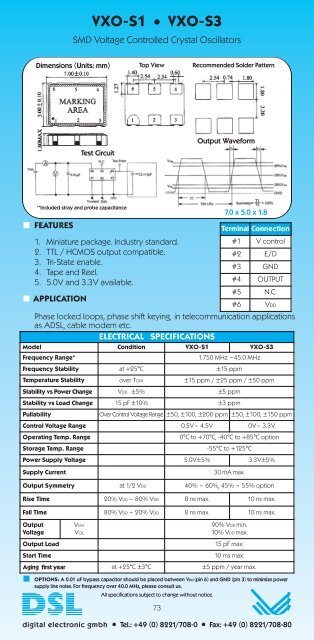
VXO-S1 • VXO-S3<br />
SMD Voltage Controlled Crystal Oscillators<br />
Dimensions (Units: mm)<br />
Top View<br />
Recommended Solder Pattern<br />
Test Circuit<br />
Output Waveform<br />
**Included stray and probe capacitance<br />
FEATURES<br />
1. Miniature package. Industry standard.<br />
2. TTL / HCMOS output compatible.<br />
3. Tri-State enable.<br />
4. Tape and Reel.<br />
5. 5.0V and 3.3V available.<br />
APPLICATION<br />
Phase locked loops, phase shift keying, in telecommunication applications<br />
as ADSL, cable modem etc.<br />
ELECTRICAL SPECIFICATIONS<br />
Model Condition VXO-S1 VXO-S3<br />
Frequency Range*<br />
All specifications subject to change without notice.<br />
7.0 x 5.0 x 1.8<br />
1.750 MHz ~45.0 MHz<br />
Frequency Stability at +25°C ±15 ppm<br />
Temperature Stability over TOPR ±15 ppm / ±25 ppm / ±50 ppm<br />
Stability vs Power Change VDD ±5% ±5 ppm<br />
Stability vs Load Change 15 pF ±10% ±3 ppm<br />
Pullability<br />
Over Control Voltage Range ±50, ±100, ±200 ppm ±50, ±100, ±150 ppm<br />
Control Voltage Range 0.5V~ 4.5V 0V~ 3.3V<br />
Operating Temp. Range<br />
Storage Temp. Range<br />
0°C to +70°C, -40°C to +85°C option<br />
-55°C to +125°C<br />
Power Supply Voltage 5.0V±5% 3.3V±5%<br />
Supply Current<br />
30 mA max.<br />
Output Symmetry at 1/2 VDD 40% ~ 60%, 45% ~ 55% option<br />
Rise Time 20% VDD ~ 80% VDD 8 ns max. 10 ns max.<br />
Fall Time 80% VDD ~ 20% VDD 8 ns max. 10 ns max.<br />
Output<br />
Voltage<br />
Output Load<br />
Start Time<br />
VOH<br />
VOL<br />
Terminal Connection<br />
#1 V control<br />
#2 E/D<br />
#3 GND<br />
#4 OUTPUT<br />
#5 N.C.<br />
90% VDD min.<br />
10% VDD max.<br />
15 pF max.<br />
10 ms max.<br />
#6 VDD<br />
Aging first year at +25°C ±3°C ±5 ppm / year max.<br />
OPTIONS: A 0.01 uF bypass capacitor should be placed between VDD (pin 6) and GND (pin 3) to minimize power<br />
supply line noise. For frequency over 40.0 MHz, please consult us.<br />
73<br />
digital electronic gmbh • Tel.: +49 (0) 8221/708-0 • Fax: +49 (0) 8221/708-80