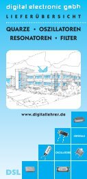
LU-QORF_6-2016

Create successful ePaper yourself
Turn your PDF publications into a flip-book with our unique Google optimized e-Paper software.
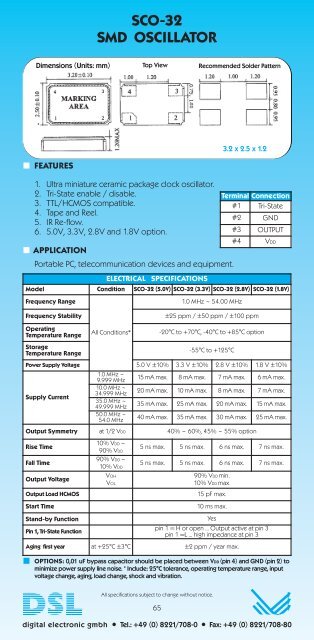
SCO-32<br />
SMD OSCILLATOR<br />
Dimensions (Units: mm)<br />
Top View<br />
Recommended Solder Pattern<br />
FEATURES<br />
3.2 x 2.5 x 1.2<br />
1. Ultra miniature ceramic package clock oscillator.<br />
2. Tri-State enable / disable.<br />
3. TTL/HCMOS compatible.<br />
4. Tape and Reel.<br />
5. IR Re-flow.<br />
6. 5.0V, 3.3V, 2.8V and 1.8V option.<br />
APPLICATION<br />
Portable PC, telecommunication devices and equipment.<br />
ELECTRICAL SPECIFICATIONS<br />
Model Condition SCO-32 (5.0V) SCO-32 (3.3V) SCO-32 (2.8V) SCO-32 (1.8V)<br />
Frequency Range<br />
Frequency Stability<br />
Operating<br />
Temperature Range<br />
Storage<br />
Temperature Range<br />
All Conditions*<br />
1.0 MHz ~ 54.00 MHz<br />
±25 ppm / ±50 ppm / ±100 ppm<br />
-20°C to +70°C, -40°C to +85°C option<br />
-55°C to +125°C<br />
Power Supply Voltage 5.0 V ±10% 3.3 V ±10% 2.8 V ±10% 1.8 V ±10%<br />
1.0 MHz ~<br />
9.999 MHz<br />
15 mA max. 8 mA max. 7 mA max. 6 mA max.<br />
10.0 MHz ~<br />
34.999 MHz<br />
20 mA max. 10 mA max. 8 mA max. 7 mA max.<br />
Supply Current<br />
35.0 MHz ~<br />
49.999 MHz<br />
35 mA max. 25 mA max. 20 mA max. 15 mA max.<br />
50.0 MHz ~<br />
54.0 MHz<br />
40 mA max. 35 mA max. 30 mA max. 25 mA max.<br />
Output Symmetry at 1/2 VDD 40% ~ 60%, 45% ~ 55% option<br />
Rise Time<br />
Fall Time<br />
Output Voltage<br />
Output Load HCMOS<br />
Start Time<br />
Stand-by Function<br />
Pin 1, Tri-State Function<br />
10% VDD ~<br />
90% VDD<br />
90% VDD ~<br />
10% VDD<br />
VOH<br />
VOL<br />
5 ns max. 5 ns max. 6 ns max. 7 ns max.<br />
5 ns max. 5 ns max. 6 ns max. 7 ns max.<br />
90% VDD min.<br />
10% VDD max.<br />
15 pF max.<br />
10 ms max.<br />
Yes<br />
pin 1 = H or open ... Output active at pin 3<br />
pin 1 =L ... high impedance at pin 3<br />
Aging first year at +25°C ±3°C ±2 ppm / year max.<br />
Terminal Connection<br />
#1 Tri-State<br />
#2 GND<br />
#3 OUTPUT<br />
#4 VDD<br />
OPTIONS: 0,01 uF bypass capacitor should be placed between VDD (pin 4) and GND (pin 2) to<br />
minimize power supply line noise. * Include: 25°C tolerance, operating temperature range, input<br />
voltage change, aging, load change, shock and vibration.<br />
All specifications subject to change without notice.<br />
65<br />
digital electronic gmbh • Tel.: +49 (0) 8221/708-0 • Fax: +49 (0) 8221/708-80