- Page 1 and 2:
Integrator Series 2 D C 5 9 0 + D C
- Page 3 and 4:
Requirements IMPORTANT Please read
- Page 5 and 6:
WARNING! - Ignoring the following m
- Page 7 and 8:
C o n t e n t s CHAPTER 1: Getting
- Page 9 and 10:
• PARAMETER SAVE 6-18 • CONFIGU
- Page 11 and 12:
• ANALOG OUTPUTS D-22 • AUTOTUN
- Page 13 and 14:
DC590+ Series DC Digital Drive A fe
- Page 15 and 16:
About this Manual This manual is in
- Page 17 and 18:
DC590+ Series DC Digital Drive P r
- Page 19 and 20:
Product Range The DC590+ Series DC
- Page 21 and 22:
1 Main drive assembly 2 Terminal co
- Page 23 and 24:
1 Main drive assembly 2 Standard do
- Page 25 and 26:
590+ Product (Frame H) Power Contro
- Page 27 and 28:
How it Works NOTE Refer to Chapter
- Page 29 and 30:
Keypads The drive is fitted with th
- Page 31 and 32:
DC590+ Series DC Digital Drive I n
- Page 33 and 34:
Mechanical Installation IMPORTANT R
- Page 35 and 36:
C A D E1 B 380A - 830A 1580A Frame
- Page 37 and 38:
Mounting the Drive NOTE General ins
- Page 39 and 40:
Installing the External Vent Kit (F
- Page 41 and 42:
Electrical Installation IMPORTANT P
- Page 43 and 44:
Minimum Connection Requirements IMP
- Page 45 and 46:
EMERGENCY STOP RELAY SIGNAL 0V SPEE
- Page 47 and 48:
EMERGENCY STOP RELAY SIGNAL 0V SPEE
- Page 49 and 50:
L1 L2 L3 3 4 Power Connections 3-Ph
- Page 51 and 52:
PE A+ Power Connections continued P
- Page 53 and 54:
FL1 Power Connections continued Ext
- Page 55 and 56:
A6 Control Connections continued Cu
- Page 57 and 58:
C1 Control Connections continued Ex
- Page 59 and 60:
A7 Control Connections continued An
- Page 61 and 62:
E1 E2 E3 E4 E5 E6 H1 H2 H3 H4 H5 H6
- Page 63 and 64:
Terminal Board - PCB Reference 4703
- Page 65 and 66:
Power Board - PCB Reference 466701
- Page 67 and 68:
Power Board - PCB Reference 466701
- Page 69 and 70:
Power Board Circuit Descriptions AH
- Page 71 and 72:
AH470330 (Frame 2) (2 Quad and 4 Qu
- Page 73 and 74:
AH385851U002, U003, U004, U005 (Fra
- Page 75 and 76:
A+ L1 L2 L3 A- D1 D2 D5 A+ L1 L2 L3
- Page 77 and 78:
A+ L1 L2 L3 A- D1 D2 D5 FS2 FS3 FS4
- Page 79 and 80:
A+ L1 L2 L3 A- SNUBBER CIRCUITS FS1
- Page 81 and 82:
AH469419 (Frame 6) Power supplies f
- Page 83 and 84:
A+ L1 L2 L3 A- EXT.A- A- FS1 FS2 FS
- Page 85 and 86:
Optional Equipment Contact your loc
- Page 87 and 88:
Assembly Procedure Figure 3- 27 Mou
- Page 89 and 90:
Speed Feedback Option Boards Each o
- Page 91 and 92:
Communications Technology Options V
- Page 93 and 94:
NOTE Metal surfaces, such as anodis
- Page 95 and 96:
Frame 6: Assembly and Installation
- Page 97 and 98:
Assembly Caution Use proper lifting
- Page 99 and 100:
Moving the AC Supply Terminals The
- Page 101 and 102:
Backplate Drilling Procedure Cover
- Page 103 and 104:
Tightening the Drive When all the b
- Page 105 and 106:
Electrical Installation IMPORTANT:
- Page 107 and 108:
Installation Drawings Drive Install
- Page 109 and 110:
Figure 3- 30 Frame 3 : 180A Stack A
- Page 111 and 112:
Figure 3- 32 Frame 4 : 380-830A Sta
- Page 113 and 114:
On the Frame 5, both the Master and
- Page 115 and 116:
Figure 3- 36 Frame H : 1200A-2700A
- Page 117 and 118:
Figure 3- 38 Frame H : 1200A-2700A
- Page 119 and 120:
Filter Installation Drawings Figure
- Page 121 and 122:
Figure 3- 42 Filter Mounting Detail
- Page 123 and 124:
Figure 3- 44 Filter Mounting Detail
- Page 125 and 126:
Figure 3- 46 Filter Mounting Detail
- Page 127 and 128:
B Parker Part Number Drive Rating W
- Page 129 and 130:
DC590+ Series DC Digital Drive O p
- Page 131 and 132:
Pre-Operation Checks Initial checks
- Page 133 and 134:
Thus the Drive can operate in two m
- Page 135 and 136:
Setting-up the Drive IMPORTANT You
- Page 137 and 138:
Selecting Speed Feedback AUXILIARY
- Page 139 and 140:
Initial Start-Up Routine Complete s
- Page 141 and 142:
Step 7: Set the Speed Setpoint(s) t
- Page 143 and 144:
Step 11: Check the STANDSTILL LOGIC
- Page 145 and 146:
Step 15: Fine adjustments for Speed
- Page 147 and 148:
Performing an Autotune • Set the
- Page 149 and 150:
Starting and Stopping Methods Stopp
- Page 151 and 152:
Control Signals Speed Demand Actual
- Page 153 and 154:
Control Signals Speed Demand Actual
- Page 155 and 156:
Advanced Starting Methods Starting
- Page 157 and 158:
DC590+ Series DC Digital Drive C o
- Page 159 and 160:
Control Loops - Principle of Operat
- Page 161 and 162:
A. If a very high motor discontinuo
- Page 163 and 164:
Field Control Set-Up Notes Use the
- Page 165 and 166:
It is the over-voltage of the back-
- Page 167 and 168:
DC590+ Series DC Digital Drive This
- Page 169 and 170:
Connecting the 6911 Keypad The Keyp
- Page 171 and 172:
Keys for Operating the Drive Locall
- Page 173 and 174:
The Menu System The menu system is
- Page 175 and 176:
Navigating the Menu System The Menu
- Page 177 and 178:
E M BASIC, STANDARD & ADVANCED STAN
- Page 179 and 180:
DIAGNOSTICS (MMI only) Parameter Ta
- Page 181 and 182:
DIAGNOSTICS (MMI only) Parameter Ta
- Page 183 and 184:
DIAGNOSTICS (MMI only) Parameter Ta
- Page 185 and 186:
ALARM STATUS Refer to Chapter 7: "T
- Page 187 and 188:
CONFIGURE DRIVE The CONFIGURE DRIVE
- Page 189 and 190:
Menu Shortcuts and Special Key Comb
- Page 191 and 192:
How to Save, Restore and Copy your
- Page 193 and 194:
DC590+ Series DC Digital Drive T r
- Page 195 and 196:
Trips and Fault Finding Trips What
- Page 197 and 198:
Calibration Checks The drive leaves
- Page 199 and 200:
Power Board Current Calibration Swi
- Page 201 and 202:
Alarm Messages When a trip occurs a
- Page 203 and 204:
When more than one trip is to be re
- Page 205 and 206:
Frame 6 Eight diagnostic LEDs indic
- Page 207 and 208:
Using the MMI to Manage Trips Trip
- Page 209 and 210:
Trip Message and Meaning Possible R
- Page 211 and 212:
Trip Message and Meaning Possible R
- Page 213 and 214:
Test Points The following test poin
- Page 215 and 216:
R o u t i n e M a i n t e n a n c e
- Page 217 and 218:
Maintenance Because of its solid st
- Page 219 and 220:
Disposal This product contains mate
- Page 221 and 222:
Repairs for Frames 4 & 5 Replacing
- Page 223 and 224:
Refitting 1. Refit the Fuse to the
- Page 225 and 226:
Replacing a Phase Assembly (Frame 6
- Page 227 and 228:
Repairs for Frame H Fuse Replacemen
- Page 229 and 230:
591+ 2Q Product (Non-Regenerative)
- Page 231 and 232:
Thyristor Suppression Board (one on
- Page 233 and 234:
DC590+ Series DC Digital Drive S e
- Page 235 and 236:
System Port (P3) This port has seve
- Page 237 and 238:
UDP XFER (TX) This is the transfer
- Page 239 and 240:
5703 Support The 5703 Setpoint Repe
- Page 241 and 242:
System Port (P3) Set-up Set MODE pa
- Page 243 and 244:
For details of the EI Bisync Protoc
- Page 245 and 246:
3. Tag Access Each parameter in the
- Page 247 and 248:
EI Binary Support This mode has man
- Page 249 and 250:
EI Bisynch Binary Message Protocol
- Page 251 and 252:
Control Character Definitions Stand
- Page 253 and 254:
EI Bisynch Binary Parameter Specifi
- Page 255 and 256:
Block 3 PNO (ID) (MN) TAG DATA FORM
- Page 257 and 258:
Block 5 PNO (ID) (MN) TAG DATA FORM
- Page 259 and 260:
Block 8 PNO (ID) (MN) TAG DATA FORM
- Page 261 and 262:
Block 13 PNO (ID) (MN) TAG DATA FOR
- Page 263 and 264:
I I I C E R T F C A T O N 1 Introdu
- Page 265 and 266:
Introduction Our Drives are certifi
- Page 267 and 268:
Provisions have been put in place s
- Page 269 and 270:
Branch Circuit/Short Circuit Protec
- Page 271 and 272:
Field Grounding Terminals The field
- Page 273 and 274:
Recommended Wire Sizes (Frame 6) Lo
- Page 275 and 276:
EMC Emissions Limits Conducted Freq
- Page 277 and 278:
EMC General Installation Considerat
- Page 279 and 280:
Issued for compliance with the EMC
- Page 281 and 282:
P a r a m e t e r S p e c i f i c a
- Page 283 and 284:
Parameter Tables The headings for t
- Page 285 and 286:
Tag Mn MMI Block Name MMI Parameter
- Page 287 and 288:
Tag Mn MMI Block Name MMI Parameter
- Page 289 and 290:
Tag Mn MMI Block Name MMI Parameter
- Page 291 and 292:
Tag Mn MMI Block Name MMI Parameter
- Page 293 and 294:
Tag Mn MMI Block Name MMI Parameter
- Page 295 and 296:
Tag Mn MMI Block Name MMI Parameter
- Page 297 and 298:
Tag Mn MMI Block Name MMI Parameter
- Page 299 and 300:
Tag Mn MMI Block Name MMI Parameter
- Page 301 and 302:
Tag Mn MMI Block Name MMI Parameter
- Page 303 and 304:
Tag Mn MMI Block Name MMI Parameter
- Page 305 and 306:
Tag Mn MMI Block Name MMI Parameter
- Page 307 and 308:
Tag Mn MMI Block Name MMI Parameter
- Page 309 and 310:
Tag Mn MMI Block Name MMI Parameter
- Page 311 and 312:
Tag Mn MMI Block Name MMI Parameter
- Page 313 and 314:
Tag Mn MMI Block Name MMI Parameter
- Page 315 and 316:
Tag Mn MMI Block Name MMI Parameter
- Page 317 and 318:
Tag Mn MMI Block Name MMI Parameter
- Page 319 and 320:
a.......ANOUT 2 (A8) [0056] Analog
- Page 321 and 322:
..........RAMP RATE [0355] Jog/Slac
- Page 323 and 324:
a...........RATE CAL [0483] Diamete
- Page 325 and 326:
..........ENCODER LINES [0024] Enco
- Page 327 and 328:
a.........INPUT 0 [0309] Setpoint S
- Page 329 and 330:
..............CALIBRATION [0239] An
- Page 331 and 332:
a...........LINK 5 ..............SO
- Page 333 and 334:
DC590+ Series DC Digital Drive P r
- Page 335 and 336:
Programming Your Application Progra
- Page 337 and 338:
The setting of the EMULATE 590P par
- Page 339 and 340:
MMI Menu Maps The function block de
- Page 341 and 342:
Compatibility with Earlier Versions
- Page 343 and 344:
Legacy implementation Version 8.x a
- Page 345 and 346:
5703 OUT This function block is use
- Page 347 and 348:
Functional Description MODE Descrip
- Page 349 and 350:
ALARM HISTORY This function block r
- Page 351 and 352:
ALARMS Parameter Tag Range Inhibits
- Page 353 and 354:
Functional Description DC590+ Serie
- Page 355 and 356:
ANALOG INPUTS Parameter Tag Range C
- Page 357 and 358:
AUTOTUNE The Autotune feature is us
- Page 359 and 360:
AUX I/O The auxiliary I/O parameter
- Page 361 and 362:
CALIBRATION Parameter Tag Range TER
- Page 363 and 364:
COMMS PORT Use this block to config
- Page 365 and 366:
CONFIGURE DRIVE This block contains
- Page 367 and 368:
CURRENT LOOP Parameter Tag Range DI
- Page 369 and 370:
CURRENT LOOP Parameter Tag Range PO
- Page 371 and 372:
CURRENT PROFILE Use this to clamp t
- Page 373 and 374:
DEMULTIPLEXER The demultiplexer fun
- Page 375 and 376:
DIAMETER CALC. Parameter Tag Range
- Page 377 and 378:
DIAMETER CALC. Parameter Tag Range
- Page 379 and 380:
*Permanently linked to Diameter Cal
- Page 381 and 382:
Static Comp Dynamic Comp Rewind (Fo
- Page 383 and 384:
Digital Input Examples Using Digita
- Page 385 and 386:
DIGITAL OUTPUTS Thes function block
- Page 387 and 388:
Using Digital Outputs with VALUE Pa
- Page 389 and 390:
DRIVE INFO Parameter Tag Range PROD
- Page 391 and 392:
ENCODER Parameter Tag Range ENCODER
- Page 393 and 394:
FEEDBACKS Diagnostics for the motor
- Page 395 and 396:
FLD WEAK VARS : MMI Sub-Menu In cer
- Page 397 and 398:
FIELD CONTROL Parameter Tag Range F
- Page 399 and 400:
FIELD AC VOLTAGE [VF (AC) RMS] Func
- Page 401 and 402:
SCALED ARMATURE VOLTAGE FEEDBACK [2
- Page 403 and 404:
LINK Use internal links to connect
- Page 405 and 406:
JOG/SLACK This block can be used to
- Page 407 and 408:
Block Diagram 0% 0% RAMP INPUT (fro
- Page 409 and 410:
LOGIC FUNC Parameter Tag Range INPU
- Page 411 and 412:
Operation Description 0-1 EDGE(A) 1
- Page 413 and 414:
Operation Description R FLIP-FLOP L
- Page 415 and 416:
MIN SPEED The Min Speed function bl
- Page 417 and 418:
MULTIPLEXER Each block collects tog
- Page 419 and 420:
OP STATION Parameter Tag Range INIT
- Page 421 and 422:
PID Parameter Tag Range POSITIVE LI
- Page 423 and 424:
Integral Gain Integral eliminates s
- Page 425 and 426:
PLL (PHASE LOCKED LOOP) The phase l
- Page 427 and 428:
PRESET SPEEDS The Preset Speeds blo
- Page 429 and 430:
Selection Table Three Boolean varia
- Page 431 and 432:
PROFILED GAIN Parameter Tag Range M
- Page 433 and 434:
RAISE/LOWER Parameter Tag Range MIN
- Page 435 and 436:
RAMPS The RAMPS parameters set the
- Page 437 and 438:
Functional Description RAMP INPUT I
- Page 439 and 440:
100% 0% RAMP INPUT % 100% 0% RAMP O
- Page 441 and 442:
SELECT Used to select a value from
- Page 443 and 444:
SEQUENCING Parameter Tag Range JOG/
- Page 445 and 446:
SETPOINT SUM Use this menu to sum a
- Page 447 and 448:
Functional Description RATIO 0 [447
- Page 449 and 450:
5. Zero speed/current disabling of
- Page 451 and 452:
SPEED LOOP Parameter Tag Range PROP
- Page 453 and 454: 105% Speed Demands The speed demand
- Page 455 and 456: SRAMP This function block limits th
- Page 457 and 458: SRAMP Parameter Tag Range ACCEL 1 J
- Page 459 and 460: STANDSTILL Parameter Tag Range AT S
- Page 461 and 462: STOP RATES Parameter Tag Range STOP
- Page 463 and 464: TEC OPTION This function block is u
- Page 465 and 466: TORQUE CALC. This block switches th
- Page 467 and 468: VALUE FUNCTION Parameter Tag Range
- Page 469 and 470: Operation Description ABS(A)> ABS(B
- Page 471 and 472: Operation Description TIMER input A
- Page 473 and 474: Operation Description UP/DOWN COUNT
- Page 475 and 476: Operation Description PROFILE SQRT
- Page 477 and 478: The Default Application Block Diagr
- Page 479 and 480: Programming Block Diagram - Sheet 2
- Page 481 and 482: Programming Block Diagram - Sheet 4
- Page 483 and 484: SCALED ARMATURE VOLTAGE FEEDBACK [2
- Page 485 and 486: FIBRE OPTIC INPUT AC TACH INPUT DC
- Page 487 and 488: DC590+ Series DC Digital Drive T e
- Page 489 and 490: Understanding the Product Code Mode
- Page 491 and 492: DC590+ Series DC Digital Drive A p
- Page 493 and 494: Technical Specifications Environmen
- Page 495 and 496: Electrical Ratings - Power Circuit
- Page 497 and 498: AC Line Choke (Frames 1-5) To corre
- Page 499 and 500: AC Line Choke (Frames 6 & H) Always
- Page 501 and 502: External Power Semiconductor Protec
- Page 503: Power Supply Fuses Power Board Iden
- Page 507 and 508: Terminal Information - Power Board
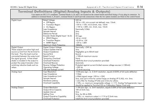
- Page 509 and 510: Terminal Information - Control Boar
- Page 511 and 512: Terminal Information - Control Boar
- Page 513 and 514: Terminal Information - Control Boar
- Page 515 and 516: Terminal Information (Frames 6 & H)
- Page 517 and 518: Wire Sizes and Termination Tighteni
- Page 519 and 520: Termination Tightening Torque (Fram
- Page 521 and 522: Common Spares Spares List (Frames 1
- Page 523 and 524: Spares List (Frames 1-5 & H) Frame
- Page 525 and 526: Spares List (Frames 1-5 & H) Frame
- Page 527 and 528: Spares List (Frame 6) 590P - Regene