T - BVU College of Engineering, Pune, India
T - BVU College of Engineering, Pune, India
T - BVU College of Engineering, Pune, India
Create successful ePaper yourself
Turn your PDF publications into a flip-book with our unique Google optimized e-Paper software.
Proceedings <strong>of</strong> the<br />
international conference on ADvances in Electronics and COnununicarions (iconAOELCO 2(07)<br />
National <strong>Engineering</strong> <strong>College</strong>, Kovilpatti. Tamilnadu, <strong>India</strong>. Feb.I-J. 2007. pp. 249 - 256<br />
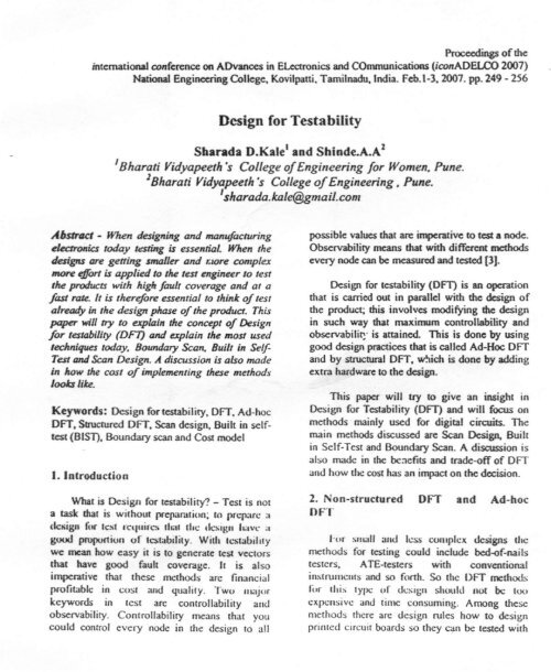
Design for Testability<br />
Sharada D.Kale t and Shinde.A.A 1<br />
IBharati Vidyapeetb's <strong>College</strong> <strong>of</strong> <strong>Engineering</strong> for Women. <strong>Pune</strong>.<br />
}Bharati Vidyapeetli's <strong>College</strong> <strong>of</strong> <strong>Engineering</strong>. <strong>Pune</strong>.<br />
'sharada.kale@gmail.com<br />
AbstrQCt - When designing and manufacturing<br />
electronics today testing is essential. When the<br />
designs are getting smaller and aore complex<br />
more effort is applied to the test engineer to test<br />
the products with high fault coverage and at a<br />
fast rate: It is therefore essential to think <strong>of</strong> test<br />
already in the design phase <strong>of</strong> the product. This<br />
paper will try to explain the concept <strong>of</strong> Design<br />
for testability (DF7) and explain the most used<br />
techniques today. Boundary Scan. Built in Self-<br />
Test and Scan Design. A discussion is also 17UJde<br />
in how the cost <strong>of</strong> implementing these method,'<br />
looks like.<br />
Keywords: Design for testability, OFT, Ad-hoc<br />
OFT, Structured OFT, Scan design, Built in selftest<br />
(BI51), Boundary scan and Cost model<br />
I. Introduction<br />
What is Design for testability? - Test is not<br />
a task that is without prepararion; (0 pn:parc a<br />
(k~i~1I fur Icst requires 11~lt lloc Iksigu have "<br />
good proportion <strong>of</strong> testability. With rcstabiluy<br />
we mean how easy it is to generate test vectors<br />
that have good fault coverage. II is also<br />
imperative that these methods are financial<br />
pr<strong>of</strong>itable in cost and quality. Two u~ljllr<br />
keywords in test arc controllability and<br />
observability. Controllability means that you<br />
could control every node in the design to all<br />
possible values that are imperative to test a node.<br />
Observability means that with different methods<br />
every node can be measured and tested (Jl.<br />
Design for testability (OFT) is an operation<br />
that is carried out in parallel with the design <strong>of</strong><br />
the product; this involves modifying the design<br />
in such way that maximum controllability and<br />
observabiliry is attained This is done by using<br />
good design practices that is called Ad-Hoc OFT<br />
and by structural OFT, w!tieh is done by adding<br />
extra hardware to the design.<br />
This paper will try to give an insight in<br />
Design for Testability (OFT) and will focus on<br />
methods mainly used for digital circuits. The<br />
main methods discussed are Scan Design, Built<br />
in Self-Test and Boundary Scan. A discussion is<br />
also made in the benefits and trade-<strong>of</strong>f <strong>of</strong> OFT<br />
and how the cost has an impact on the decision.<br />
2. Non-structured OFT and Ad-hoc<br />
OFT<br />
I"Of small and less complex designs the<br />
methods for testing could include bed-<strong>of</strong>-nails<br />
testers, ATfi-testers with conventional<br />
instruments and so forth, So the DFT methods<br />
lor this typc or design should not be 10(1<br />
expensive and time consuming. Arnong these<br />
methods there arc design rules how to design<br />
printed circuit boards so they can be tested with
Sharada Kale and Shinde<br />
bed-<strong>of</strong>-nail testers as well as general design rules<br />
how to design a circuit so that it is easier to<br />
test (I).<br />
2.1. Design Rules for PCBs<br />
On a PCB almost all errors is <strong>of</strong> the type<br />
shorts or opens. To detect short between<br />
networtcs, one must access each net at a single<br />
point, which can be chosen at the must<br />
convenient point. To detect opens each net-end<br />
must be accessed. this test is the most difficult<br />
for a bed-<strong>of</strong>-nails tester.<br />
Insulation test - It is essential that each net<br />
have at least one access on each net where the<br />
nail or probe can be placed. Continuity test - At<br />
the end <strong>of</strong> each net an access point mU~1be place<br />
to make it possible to test all opens. If possible<br />
avoid using packages with to small pitch which<br />
makes it harder to get test points within a<br />
reasonable distance. Also if possible avoid<br />
placing two or more dense component close to<br />
each other and also try to place them on the<br />
periphery <strong>of</strong> the board.<br />
2.2. Ad-hoc DFT<br />
Ad-hoc design for testability relies on<br />
"good' design practices learnt through<br />
experience are used as guidelines:<br />
• Avoid asynchronous (un-clocked) feedback.<br />
• Make flip-flops initializable<br />
• A void redundant gates. A void large 1;111ill<br />
gates.<br />
• Provide test control for difficult-to-control<br />
signals.<br />
• A void gated clocks.<br />
• Consider ATE requirements (tristarcs. ctc.)<br />
• Separate digital circuitry from analogue.<br />
• Divide large logic blocks into smaller ones,<br />
which can N: selected.<br />
• Avoid circuitry with large sequential depth.<br />
~' \<br />
250<br />
iconADELCO 2007<br />
These techniques can be used for small<br />
designs but when designs get bigger the design is<br />
hard to get an overview <strong>of</strong> and these methods are<br />
approximate and do not always point to the<br />
source <strong>of</strong> the testability problem.<br />
As the size and complexity <strong>of</strong> digital<br />
systems are getting larger alternative forms <strong>of</strong><br />
design for testability is getting popular. These<br />
methods are called structured OFT_ In structured<br />
OFT extra logic is included in the design to<br />
easily test a circuit. Among these methods scan<br />
design, Built in Self-Test and Boundary Scan are<br />
commonly used.<br />
3, Scan Design<br />
In a scqucnt.al circuit it is difficult to fonn<br />
test vectors fur stuck-at-faults because the<br />
sequential depth <strong>of</strong> the design easily makes the<br />
test vectors to large. The main idea with sean<br />
design is to obtain control and observability for<br />
flip-flops and' thus making it easier to form test<br />
vectors. Adding a test mode to the circuits such<br />
that when the circuit is in test mode, all flip-flops<br />
functionality forms one or more shift registers<br />
does this. Controllability is achieved in test mode<br />
by setting the flip-flops to any desired state by<br />
shifting in the required state into the shift register<br />
(also known as scan register). The states <strong>of</strong> the<br />
flip-flops are observed by shifting the contents <strong>of</strong><br />
the scan register out. The states <strong>of</strong> all flip-flops<br />
in a design can be set or observed in a number <strong>of</strong><br />
clock cycles that equals the number <strong>of</strong> flip-flops<br />
in the longest scan register J2 J.<br />
3.1. Scan Cells<br />
The theory <strong>of</strong> SC
I<br />
l<br />
Design for Testability<br />
500 port may be connected to the Q or Qnegative<br />
ports.<br />
Agure 1. Mux-O Flip-Flop<br />
It is important to ensure that external control<br />
signals do not interfere with the flip-flop (Figure<br />
2) when it is in scan mode (I].<br />
Figure 2. Set-Scan Flip-Flop<br />
251<br />
icon AOELCO 2007<br />
• Operate: Normal transparent operation <strong>of</strong><br />
the element, 0 to Q and QN.<br />
..Scan Sample: Observability <strong>of</strong>1he logic that<br />
fans into the scan element, 0 to 500.<br />
•. Scan LoadIShift Serially IoadIshift data into<br />
the scan chain while unloading the last<br />
sample. SOl to SOO .<br />
• .Scan Data Apply: Control the output <strong>of</strong> the<br />
scar. element and thereby controlling the<br />
logic attached to Q.<br />
.H'l...·t<br />
..•...: .._-_ .. 1.- i-·. :<br />
"'~:<br />
'.cbr••••.••~<br />
••••••• ~f •••.<br />
"<br />
'.' i F+-<br />
~<br />
i:'--;<br />
--'<br />
1<br />
I<br />
!:.<br />
• ~ .0(,'\."<br />
..,...~.. \ •..•...<br />
------- ••.••.. (W-.<br />
Figure 3, Full-Scan chain (1)<br />
The signal path <strong>of</strong> the flip-flop can be<br />
controlled and observed by four transfer<br />
. functions.<br />
3.2. Partial Scan<br />
When all flip-flops in a design can be<br />
controlled and observed with scan cells is called
Sharada Kale and Shinde<br />
full-scan (Figure 3). In a circuit with a lot <strong>of</strong><br />
sequential feedback and thereby the: length <strong>of</strong> the<br />
sequences cannot be bounded it is not advisable<br />
to use scan flip-flops. In particular parts <strong>of</strong> the<br />
design where timing is critical it can also be<br />
advisable to not using scan flip-flops. In these<br />
cases the design is called partial scan. When this<br />
type <strong>of</strong> design is run through an ATI'G-tool it<br />
may cause loss <strong>of</strong> fault coverage. increased<br />
runtime and an increase in the number <strong>of</strong> tc"S(<br />
vector generated.<br />
3-3. Multiple Scan Chains<br />
If many flip-flops are used in a design a<br />
single scan chain can become too large. It call<br />
take very long time to load each state with a very<br />
long scan chain. Splitting the chain in more scan<br />
chains can solve this. The trade-<strong>of</strong>fs <strong>of</strong> this<br />
solution is that multiple scan chain." requires<br />
more dedicated (cest pins. If multiple scan chains<br />
are used the scan chains should have the same<br />
number <strong>of</strong> scan bits as far as possible this IS<br />
called balanced scan chains.<br />
This is the rncst cost efficient method and it<br />
uses the memory more efficient<br />
3.4. Scan Design Rules<br />
The 'e are many rules <strong>of</strong> for designing a<br />
scan-based design among allthcsc four is useful:<br />
• Use only one kind <strong>of</strong> flip.flop in the design.<br />
E.g. D-type:master-slave.<br />
• At least one primary input pin must be<br />
available for test.<br />
• .Every flip-flop clock must be controllable<br />
from primary inputs.<br />
• Avoid synchronous latches, transparent<br />
latches.<br />
• Do not feed clock to data inputs <strong>of</strong> f1ip- flops<br />
4. Built in Self Test<br />
252<br />
iconADELCO 2007<br />
Since circuits become more dense and faster<br />
with smaller size and that the logic-to-pin ratio<br />
on chips is increasing makes the testing <strong>of</strong> logic<br />
morc and more difficult. It takes longer time to<br />
generate test patterns and the patterns consume<br />
lot <strong>of</strong> memory. Often are the designers not aware<br />
<strong>of</strong> the gate-level structure <strong>of</strong> their designs<br />
because it is synthesized in VHDL hardware<br />
description languages. Therefore it has becoming<br />
interesting to implement different kind <strong>of</strong> logic<br />
in the design so it can test itself so called BIST.<br />
Figure 4. Built in self test (3]<br />
The idea <strong>of</strong> BIST is to implement test<br />
pattern generation and response analyzing and<br />
even fault analyzing together with the chip. BIST<br />
(Figure 4) can be categorized in different ways:<br />
Online IlIST: Testing is done during normal<br />
operation<br />
• Concurrent testing - detects faults while<br />
system is doing normal functions..<br />
e Nun-Concurrent testing - detects faults<br />
while system is in idle mode.<br />
Offline BIST: System is brought 10 a test<br />
mode<br />
e. functional testing - tests the system at a<br />
high level <strong>of</strong> function.<br />
e Structural testing - detects structural faults<br />
<strong>of</strong> the system.<br />
4.1. BIST Pattern Generation
/<br />
Design for Testability<br />
The size <strong>of</strong> the BIST logic should not be too<br />
large compared to the rest <strong>of</strong> the logic otherwise<br />
the BIST logic can have more errors than the<br />
usable circuit. The design <strong>of</strong> the BIST should be<br />
in the order <strong>of</strong> 20"~ to be efficient. Because <strong>of</strong><br />
this the test patterns cannot take up to much<br />
memory space so !hey must be compressed<br />
somehow. The design must have a simple<br />
hardware implementation and it should not slow<br />
down the nonnal operation. Different kinds <strong>of</strong><br />
hardware for pattern generation can be used can<br />
be used, the most preferred is LFSR - linear<br />
feedback shift register (Figure S).<br />
.,., ." ..-<br />
Figure 5. LFSR<br />
"<br />
Different kinds <strong>of</strong> methods for pattern<br />
generation can be used.<br />
4.1.1. Exhaustive Testing. Every test pattern<br />
are applied to the circuit. which requires 2. test<br />
patterns. It can be implemented using a binary<br />
counter or a maximum length autonomous<br />
LFSR. This method is considered ouly when<br />
0
Sharada Kale and Shinde<br />
generator, a testing response compactor and a<br />
scan chain cell (2J.<br />
S. Boundary Scan<br />
Almost all printed circuit boards today is <strong>of</strong><br />
the type multilayer SMT·boards with a lot <strong>of</strong><br />
circuitry in between the layers and components<br />
soldered on both sides. Many components used<br />
today are not easily accessible because they have<br />
their connections under their package e.g. SP and<br />
BOA circuits. This makes it difficult to use in<br />
circuit test systems with nails. In circuit testers<br />
also has the disadvantage that the stress<br />
components during testing. All these problems<br />
has led to a standard for testing components on<br />
PCBs, this standard is called ITAG 1149.1<br />
Boundary-scan Design Standard. Boundaryscan<br />
operates under two major modes:<br />
• Non-invasive mode: In this mode the circuit<br />
is guaranteed to work independent from the<br />
rest <strong>of</strong> the logic in the IC. This makes it<br />
pos- ible for the circuit to serially shifting in<br />
and out data from the circuit. These<br />
activities do not affect the normal behavior<br />
<strong>of</strong> the circuit.<br />
• Pin permission modes: This mode takes<br />
control <strong>of</strong> the input and output pins <strong>of</strong> the<br />
IC, thus making it possible to test the<br />
interconnections <strong>of</strong> the IC separately from<br />
the system logic. This mode disrupts the<br />
normal behavior <strong>of</strong> the circuit. For Ie's to<br />
work under the 1149.1 standard they must<br />
start-up in non-invasive mode so the Ie is<br />
not damaged. When running the Ie in the<br />
pin permission modes care must be taken<br />
when returning to non-invasive mode.<br />
Accidentally driving a bus simultaneously<br />
with 'I's and '0'5 can easily occur<br />
5.1. Configuration <strong>of</strong> Boundary Scan<br />
Components<br />
254<br />
iconADELCO 2007<br />
On an integrated circuit compliant with the<br />
standard each pin has a boundary-scan cell, all<br />
these cells are connected in series to form a<br />
boundary register. The first cell in the chain is<br />
connected to the input pin TDI (fest Data In)<br />
and the last cell is connected to the output pin<br />
TOO (Test Data Out). DiffCRtlt kinds <strong>of</strong><br />
registers can be connected between the TOI and<br />
TOO pins. The device 10 register provides the<br />
identification <strong>of</strong> the circuit, the Bypass register<br />
makes it possible to reduce the length <strong>of</strong> the<br />
register when a specific IC is (lot used for a test,<br />
The Instruction register can' be loaded with<br />
instructions, which enables different modes <strong>of</strong><br />
the hardware. The TAP-controller is a simple<br />
finite state machine that recognizes the<br />
boundary-scan protocol and controls the<br />
operation <strong>of</strong> the hardware through internal<br />
signals, The only signals that are allowed to<br />
influence the TAP controller is the test clock<br />
(TCK)-, test mode select (TMS)- and the Test<br />
reset (TRST)- pins. (Figure 6) When connecting<br />
many circuits a boundary-scan chain is created,<br />
this chain can be configured in many different<br />
ways.<br />
Figure 6. Boundary Scan<br />
S.2. Test Instructions
Design for Testability<br />
To control the system various rest<br />
instructions are used among these some can be<br />
used for other purposes than testing.<br />
SAMPLEIPRELOAO - (required) with this<br />
instruction it is possible to take a sample <strong>of</strong> the<br />
components input and output signals and it is<br />
also possible to load the boundary scan register<br />
with this value.<br />
EXTEST - (required) this instruction makes it<br />
possible to test circuits independently <strong>of</strong>f the<br />
chip since it captures the signals coming into the<br />
chip and driving the circuits with signals from<br />
the boundary-scan register.<br />
BYPASS - (required) With the BYPASS<br />
instruction it is possible to use shorter boundaryscan<br />
vectors if the particular '\OlTlp')nentis not<br />
used by certain tests. .<br />
lNTEST - (optional) with this instruction It IS<br />
possible to shifting in and out tests vectors and<br />
test data from the on chip logic.<br />
RUNBIST - (optional) The purpose <strong>of</strong><br />
RUNBIST is to control on-chip logic BIST via<br />
the boundary-scan chain.<br />
CLAMP - (optional) This instruction is used<br />
when forcing the output pins to be driven by the<br />
boundary-scan register.<br />
IDCOOE - The component has a code, which<br />
contains the identification <strong>of</strong> the component; this<br />
is called a JEOEC code. The instruction puts this<br />
data between TOI and TOO so that it can be<br />
shifted out. This instruction is required when<br />
components have JEDEC codes.<br />
255<br />
icon ADELCO 2007<br />
USERCODE - When using user programmable<br />
components such as FrGAs this instruction is<br />
used to load the device identification register<br />
with the code that the user has prograrmned into<br />
the component. This instruction is required when<br />
user programmable component has a device 10<br />
register.<br />
HIGHZ - This instruction puts all output pins<br />
into high impedance state that prevents damage<br />
to the on-system logic and protects other<br />
components as well.<br />
5.3. Boundary Scan Cells<br />
The boundary scan cells could look different<br />
depending on the function <strong>of</strong> the component.<br />
Control and observe cell - The normal type <strong>of</strong><br />
boundary scan cell (Figure 7).<br />
Figure 7. Control-and-Observe Scan Cell<br />
Observe only cell - If the cell should only<br />
sample the signal it is only necessary to use an<br />
Observe only cell. Bi-directional pins (Figure 8).<br />
If the component has bidirectional pins the cell<br />
must have three cells to take care <strong>of</strong> these<br />
signals. Since a component with a lot <strong>of</strong><br />
bidirectional pins requires many cells it is<br />
possible to control these tri-state cells with one<br />
enable signal. But special care must be taken so<br />
that one does not use a scan register both to<br />
control an output pin and as an input to the<br />
system logic.
-<br />
I I<br />
, 5,5,<br />
r .<br />
i: ,1<br />
f I<br />
'-<br />
Sharada Kale and Shinde<br />
l EN '<br />
~-T-~.!:'·<br />
-- •.... _-_.j<br />
Figure 8. Bi-directional pin<br />
5.4. Boundary<br />
Language<br />
Scan Description<br />
To communicate the infonnation about the<br />
boundary scan hardware to users <strong>of</strong> a particular<br />
chip and to CAD-tools through the VHOL<br />
hardware description language a Boundary Scan<br />
Description Language (UDSL) was added to the<br />
1149.1 standard. BOSL can be used by ATPGtools<br />
to generate test patterns and by synthesis<br />
tools to synthesize test logic but are not usable as<br />
a simulation model, since it can not describe<br />
voltages, currents and so forth.<br />
Pros and Cons<br />
+ Less overhead than Scan design<br />
+ Less expensive test equipment<br />
+ IC's tested at their complete, interconnected<br />
environment<br />
- Circuits with boundary scan are expensive<br />
and they can be hard to find<br />
Requires quite expensive s<strong>of</strong>tware<br />
and equipment<br />
6. Benefits and 1 rade-<strong>of</strong>fs <strong>of</strong> OFT<br />
The major benefits <strong>of</strong> using Design for<br />
testability are:<br />
256<br />
iconADELCO 2007<br />
• Shorter time to market<br />
• Reduced test time<br />
• Inexpensive test equipment<br />
• Yield learning, which is <strong>of</strong>ten overlooked<br />
The implementation <strong>of</strong> OFT involves some<br />
sacrifices.<br />
• Increased area <strong>of</strong> components<br />
• More pins on the I'eu<br />
• Increased PCB area<br />
• Degraded performance <strong>of</strong> the circuit.<br />
It is up 10 each cOlllpany to decide if the<br />
product they producing can benefit on applying<br />
OFT or not.<br />
7. Conclusion<br />
This paper has tried to give an insight in<br />
design for testability. The main ideas used today<br />
arc Scan design. built in self-test and Boundary<br />
scan. The difficulties in choosing methods are<br />
dependent <strong>of</strong> a lot <strong>of</strong> factors to get the most<br />
benefit-to-cost ratio. There are cost models used<br />
that try to help in this decision. To apply OFT or<br />
not apply OFf is dependent on factors like<br />
quality and volume.<br />
References<br />
[I) Alfred L. Crouch, "Design-for-test", Prentice<br />
Hall PTR 1999.<br />
(2) RooD. (Shawn) Blanton and Wojciech Maly.<br />
"Design for testability model", www.ece<br />
Cost.cmu.edulcssi/resbooklpdf/wei2.pdf.<br />
(3) Michael L Bushnell and Vishwani D. Agrawal,<br />
"Essentials <strong>of</strong> Electronic Testing ", Kluwer<br />
Academic Publishers 200 I


