QUANTAR™ Instruction Manuals - The Repeater Builder's Technical ...
QUANTAR™ Instruction Manuals - The Repeater Builder's Technical ...
QUANTAR™ Instruction Manuals - The Repeater Builder's Technical ...

Create successful ePaper yourself
Turn your PDF publications into a flip-book with our unique Google optimized e-Paper software.
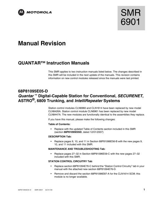
Manual Revision 1<br />
QUANTAR <strong>Instruction</strong> <strong>Manuals</strong><br />
SMR<br />
6901<br />
This SMR applies to two instruction manuals listed below. <strong>The</strong> changes described in<br />
this SMR will be included in the next update of the manuals. This revision contains<br />
information on new control modules released since the manuals were last printed.<br />
68P81095E05-D<br />
Quantar Digital-Capable Station for Conventional, SECURENET,<br />
ASTRO ® , 6809 Trunking, and Intelli<strong>Repeater</strong> Systems<br />
Station control modules CLN6960 and CLN1614 have been replaced by new model<br />
CLN8426A. Station control module CLN6961 has been replaced by new model<br />
CLN8447A. <strong>The</strong> new modules are functionally identical to the assemblies they replace.<br />
If you have this manual, please make the following changes:<br />
Table of Contents:<br />
• Replace with the updated Table of Contents section included in this SMR<br />
(section 68P81095E05D, dated 12/01/2007)<br />
DESCRIPTION Tab:<br />
• Replace pages 9, 10, and 11 in Section 68P81096E56-B with the new pages 9,<br />
10, and 11 included with this SMR.<br />
MAINTENANCE AND TROUBLESHOOTING Tab:<br />
• Replace pages 27–32 in Section 68P81096E59-C with the new pages 27–32<br />
included with this SMR.<br />
STATION CONTROL CIRCUITRY Tab:<br />
• Replace section 68P81094E76-C behind the “Station Control Circuitry” tab in your<br />
manual with the attached new section 68P81094E76-D.<br />
• Remove and discard the section 68P81096E87-A for the CLN1614 SCM; this<br />
module is no longer available.<br />
68P81095E05-D SMR-6901 02/01/08 1
68P81094E85-O<br />
ASTRO-TAC Receiver For Analog/ASTRO ® and Analog/<br />
SECURENET Systems<br />
Station control modules TTN4094A/B and TRN7900A/B have been replaced by new<br />
models CLN8426A and CLN8447A. <strong>The</strong> new modules are functionally identical to the<br />
assemblies they replace.<br />
If you have this manual, please make the following changes:<br />
DESCRIPTION Tab:<br />
• <strong>The</strong> following paragraph replaces the “Introduction” paragraph on page 6:<br />
<strong>The</strong> Station Control Module (SCM) is the microprocessor – based controller for<br />
the station. Major components include an MC68360 microprocessor, a 56311<br />
Digital Signal Processor (DSP), and two programmable devices, a CPLD for the<br />
host and a FPGA for the DSP. <strong>The</strong> SCM operates as follows:<br />
• Replace all occurrences of “DSP ASIC” with “DSP FPGA”. <strong>The</strong> SCM now uses a<br />
field-programmable gate array (FPGA) instead of an application-specific IC<br />
(ASIC).<br />
STATION CONTROL CIRCUITRY Tab:<br />
• Replace section 68P81090E94-O behind the “Station Control Circuitry” tab in your<br />
manual with the attached new section 68P81094E76-D.<br />
<strong>The</strong> remaining pages of this SMR are not needed for 68P81094E85-O and may be<br />
discarded.<br />
2 02/01/08 SMR-6901 68P81095E05
QUANTAR ®<br />
Digital - Capable Station<br />
For Conventional, SECURENET, ASTRO,<br />
6809 Trunking, and Intellirepeater Systems<br />
VHF - 25W & 125W<br />
UHF - 25W, 100W & 110W<br />
800 MHz - 20W &100W<br />
900 MHz - 100W<br />
<strong>Instruction</strong> Manual<br />
68P81095E05-D
Computer Software Copyrights<br />
<strong>The</strong> Motorola products described in this document include a copyrighted Motorola computer program. Laws in the United States and other<br />
countries, as well as International Treaties, preserve for Motorola the exclusive rights for Motorola’s copyrighted computer programs, including<br />
the exclusive right to copy, reproduce, distribute, or otherwise transfer said computer program(s). Accordingly, the copyrighted Motorola<br />
computer programs contained in this document may not be copied, decompiled, reverse engineered, or reproduced in any manner and on or<br />
within any media without the express written permission of Motorola. Furthermore, the purchase of Motorola products shall not be deemed to<br />
grant either directly or by implication, estoppel, or otherwise, any license under the copyrights, patents, or patent applications of Motorola,<br />
except for the normal non-exclusive, royalty-free license to use that arises by operation of law in the sale of a product.<br />
Document Copyrights<br />
© Motorola, Inc. All rights reserved.<br />
No duplication or distribution of this document or any portion thereof shall take place without the express written permission of Motorola. No part<br />
of this document may be reproduced, distributed, or transmitted in any form or by any means, electronic or mechanical, for any purpose without<br />
the express written permission of Motorola.<br />
To order additional copies of this document contact your Motorola sales representative.<br />
Disclaimer<br />
<strong>The</strong> information in this document is carefully examined, and is believed to be entirely reliable. However, no responsibility is assumed for<br />
inaccuracies. Furthermore, Motorola reserves the right to make changes to any products herein to improve readability, function, or design.<br />
Motorola does not assume any liability arising out of the applications or use of any product or circuit described herein; neither does it cover any<br />
license under its patent rights nor the rights of others.<br />
Trademark Information<br />
<strong>The</strong> following are registered trademarks of Motorola, Inc.: Motorola, the Motorola logo, ASTRO, ASTRO-TAC, EMBASSY, FullVision,<br />
INTELLIREPEATER, QUANTAR, QUANTRO, and SMARTZONE.<br />
<strong>The</strong> following are Motorola trademarks: CENTRACOM Elite, CENTRACOM Series, CENTRACOM Gold Series, MOSCAD, SECURENET, and<br />
Wireless Network Gateway.<br />
HP, HP-UX, OpenView, Vectra, and Hewlett Packard are registered trademarks of Hewlett-Packard Corporation.<br />
UNIX is a registered trademark of <strong>The</strong> Open Group in the United States and other countries.<br />
Any other brand or product names are trademarks or registered trademarks of their respective holders.<br />
WARRANTY<br />
Limited Software Warranty<br />
For the first ninety (90) days following its initial shipment, Motorola warrants that when properly used, its software will be free from reproducible<br />
defects that cause a material variance from its published specification. However, Motorola does not warrant that program operation will be<br />
uninterrupted or error- free, that each defect will be corrected, or that any program will meet Licensee’s particular requirements.<br />
This warranty does not cover an item of Software (i) used in other than its normal and customary manner; (ii) subjected to misuse; or (iii)<br />
subjected to modifications by Licensee or by any party other than Motorola without the prior written consent of Motorola.<br />
Limited Media Warranty<br />
For the first ninety (90) days following its initial shipment, Motorola warrants that the media carrying the software will be free from defects that<br />
damage the performance of the software. Motorola will replace any damaged media free of charge during the warranty period. Warranted media<br />
is limited to that which is used to transport the software (such as floppy disks and authorization key). PROMs that may store the software in<br />
equipment are not covered under this warranty.<br />
Limitation of Liability<br />
Motorola’s total liability and Licensee’s sole remedy for any warranted software shall be limited to, at Motorola’s option, software replacement or<br />
the payment of Licensee’s actual damages, not to exceed the total licensed charge paid by Licensee to Motorola for the item of software that<br />
caused the damage.<br />
<strong>The</strong> warranties set forth above extend only to the first licensee. Subsequent transferees accept these programs “as is” and without warranties of<br />
any kind. This warranty is given in lieu of all other warranties, express or implied, including, without limitation, the warranties of<br />
merchantability and fitness for a particular purpose.<br />
In no event shall Motorola be liable for special, incidental, or consequential damages (including, without limitation, loss of use, time or data,<br />
inconvenience, commercial loss, and lost profits or savings) to the full extent that such may be disclaimed by law even if Motorola has been<br />
advised of the possibility of such damage against licensee by any other party.<br />
Repair of Defects<br />
<strong>The</strong> classification of defects in Motorola-supplied software shall be the responsibility of Motorola. Remedy of defects is at the sole discretion of<br />
Motorola. If Motorola agrees to remedy a software defect, the new software will be warranted until the end of the original limited warranty period.<br />
Replacement of any software defect shall constitute Motorola supplying the Licensee with the appropriate software media and authorization<br />
key. Field installation and configuration are not included. Field software updates/upgrades and new enhancement option software will be<br />
warranted for ninety (90) days from the date of initial shipment.<br />
All warranty service will be performed at service locations designated by Motorola. Travel and associated expenses of the Licensee or such<br />
expenses incurred by Motorola for visits to Licensee’s location by Motorola personnel are not covered by this warranty.
Table of Contents<br />
QUANTAR ®<br />
Digital–Capable Station<br />
for Conventional, ASTRO,<br />
6809 Trunking, and Intelli<strong>Repeater</strong> Systems<br />
VHF — 25W & 125W<br />
UHF — 25W, 100W, & 110W<br />
800 MHz — 20W & 100W<br />
900 MHz — 100W<br />
Model/Option Information . . . . . . . . . . . . . . . . . . . . . . . . . . . . . . . . . . . . . . . . . . . . . . . . . . . . . . . . . . . . . . . . . . . . . . . . xi<br />
Foreword . . . . . . . . . . . . . . . . . . . . . . . . . . . . . . . . . . . . . . . . . . . . . . . . . . . . . . . . . . . . . . . . . . . . . . . . . . . . . . . . . . . xxiv<br />
General Safety Information . . . . . . . . . . . . . . . . . . . . . . . . . . . . . . . . . . . . . . . . . . . . . . . . . . . . . . . . . . . . . . . . . . . . . xxvi<br />
Performance Specifications . . . . . . . . . . . . . . . . . . . . . . . . . . . . . . . . . . . . . . . . . . . . . . . . . . . . . . . . . . . . . . . . . . . . .xxviii<br />
DESCRIPTION . . . . . . . . . . . . . . . . . . . . . . . . . . . . . . . . . . . . . . . . . . . . . . . . . . . . . . . . . . . . . . . . . . 68P81096E56<br />
Introduction . . . . . . . . . . . . . . . . . . . . . . . . . . . . . . . . . . . . . . . . . . . . . . . . . . . . . . . . . . . . . . . . page 1<br />
Compact Mechanical Design . . . . . . . . . . . . . . . . . . . . . . . . . . . . . . . . . . . . . . . . . . . . . . . . . . . . . . . . . . . . . . . . . . page 1<br />
State-of-the-Art Electrical Design . . . . . . . . . . . . . . . . . . . . . . . . . . . . . . . . . . . . . . . . . . . . . . . . . . . . . . . . . . . . . . page 2<br />
Summary of Operating Features . . . . . . . . . . . . . . . . . . . . . . . . . . . . . . . . . . . . . . . . . . . . . . . . . . . . . . . . . . . . . . . page 3<br />
Multiple System Capability. . . . . . . . . . . . . . . . . . . . . . . . . . . . . . . . . . . . . . . . . . . . . . . . . . . . . . . . . . . . . . . . . . . . page 4<br />
Station Components . . . . . . . . . . . . . . . . . . . . . . . . . . . . . . . . . . . . . . . . . . . . . . . . . . . . . . . . . page 6<br />
Functional <strong>The</strong>ory of Operation . . . . . . . . . . . . . . . . . . . . . . . . . . . . . . . . . . . . . . . . . . . . . . . . page 8<br />
Transmitter Circuitry Operation . . . . . . . . . . . . . . . . . . . . . . . . . . . . . . . . . . . . . . . . . . . . . . . . . . . . . . . . . . . . . . . . page 5<br />
Receiver Circuitry Operation . . . . . . . . . . . . . . . . . . . . . . . . . . . . . . . . . . . . . . . . . . . . . . . . . . . . . . . . . . . . . . . . . . page 9<br />
Station Control Circuitry Operation . . . . . . . . . . . . . . . . . . . . . . . . . . . . . . . . . . . . . . . . . . . . . . . . . . . . . . . . . . . . . page 9<br />
Wireline Interface Board Operation . . . . . . . . . . . . . . . . . . . . . . . . . . . . . . . . . . . . . . . . . . . . . . . . . . . . . . . . . . . . page 10<br />
Power Supply Module Operation . . . . . . . . . . . . . . . . . . . . . . . . . . . . . . . . . . . . . . . . . . . . . . . . . . . . . . . . . . . . . . page 10<br />
INSTALLATION . . . . . . . . . . . . . . . . . . . . . . . . . . . . . . . . . . . . . . . . . . . . . . . . . . . . . . . . . . . . . . . . . 68P81096E57<br />
Pre-Installation Considerations . . . . . . . . . . . . . . . . . . . . . . . . . . . . . . . . . . . . . . . . . . . . . . . . page 2<br />
Installation Overview . . . . . . . . . . . . . . . . . . . . . . . . . . . . . . . . . . . . . . . . . . . . . . . . . . . . . . . . . . . . . . . . . . . . . . . . page 2<br />
Environmental Conditions at Intended Site . . . . . . . . . . . . . . . . . . . . . . . . . . . . . . . . . . . . . . . . . . . . . . . . . . . . . . . page 3<br />
Equipment Ventilation . . . . . . . . . . . . . . . . . . . . . . . . . . . . . . . . . . . . . . . . . . . . . . . . . . . . . . . . . . . . . . . . . . . . . . . page 3<br />
AC Input Power Requirements . . . . . . . . . . . . . . . . . . . . . . . . . . . . . . . . . . . . . . . . . . . . . . . . . . . . . . . . . . . . . . . . page 4<br />
Equipment Mounting Methods . . . . . . . . . . . . . . . . . . . . . . . . . . . . . . . . . . . . . . . . . . . . . . . . . . . . . . . . . . . . . . . . . page 4<br />
Site Grounding and Lightning Protection . . . . . . . . . . . . . . . . . . . . . . . . . . . . . . . . . . . . . . . . . . . . . . . . . . . . . . . . . page 5<br />
Recommended Tools and Equipment . . . . . . . . . . . . . . . . . . . . . . . . . . . . . . . . . . . . . . . . . . . . . . . . . . . . . . . . . . . page 6<br />
Equipment Unpacking and Inspection . . . . . . . . . . . . . . . . . . . . . . . . . . . . . . . . . . . . . . . . . . . . . . . . . . . . . . . . . . . page 6<br />
Physical Dimensions and Clearances . . . . . . . . . . . . . . . . . . . . . . . . . . . . . . . . . . . . . . . . . . . . . . . . . . . . . . . . . . . page 7<br />
Mechanical Installation . . . . . . . . . . . . . . . . . . . . . . . . . . . . . . . . . . . . . . . . . . . . . . . . . . . . . . page 14<br />
Unpacking the Equipment . . . . . . . . . . . . . . . . . . . . . . . . . . . . . . . . . . . . . . . . . . . . . . . . . . . . . . . . . . . . . . . . . . . page 14<br />
Mounting Procedures. . . . . . . . . . . . . . . . . . . . . . . . . . . . . . . . . . . . . . . . . . . . . . . . . . . . . . . . . . . . . . . . . . . . . . . page 20<br />
Stacking Cabinets . . . . . . . . . . . . . . . . . . . . . . . . . . . . . . . . . . . . . . . . . . . . . . . . . . . . . . . . . . . . . . . . . . . . . . . . . page 25<br />
Stacking Modular Racks . . . . . . . . . . . . . . . . . . . . . . . . . . . . . . . . . . . . . . . . . . . . . . . . . . . . . . . . . . . . . . . . . . . . page 26<br />
Anti-Vibration/EMI Screws . . . . . . . . . . . . . . . . . . . . . . . . . . . . . . . . . . . . . . . . . . . . . . . . . . . . . . . . . . . . . . . . . . . page 27<br />
Networks & Enterprise<br />
©Motorola, Inc. 2008 SMR-6901 68P81095E05-D<br />
All Rights Reserved<br />
Printed in U.S.A.<br />
1301 E. Algonquin Schaumburg, IL 60196<br />
02/01/08–UP
Electrical Connections . . . . . . . . . . . . . . . . . . . . . . . . . . . . . . . . . . . . . . . . . . . . . . . . . . . . . . page 28<br />
Power Supply Connections . . . . . . . . . . . . . . . . . . . . . . . . . . . . . . . . . . . . . . . . . . . . . . . . . . . . . . . . . . . . . . . . . . page 28<br />
RF Cabling Connections . . . . . . . . . . . . . . . . . . . . . . . . . . . . . . . . . . . . . . . . . . . . . . . . . . . . . . . . . . . . . . . . . . . . page 32<br />
Connecting System Cables . . . . . . . . . . . . . . . . . . . . . . . . . . . . . . . . . . . . . . . . . . . . . . . . . . . . . . . . . . . . . . . . . . page 38<br />
Connecting Telephone Lines . . . . . . . . . . . . . . . . . . . . . . . . . . . . . . . . . . . . . . . . . . . . . . . . . . . . . . . . . . . . . . . . . page 46<br />
Connecting V24 Modems. . . . . . . . . . . . . . . . . . . . . . . . . . . . . . . . . . . . . . . . . . . . . . . . . . . . . . . . . . . . . . . . . . . . page 50<br />
Connecting External Reference . . . . . . . . . . . . . . . . . . . . . . . . . . . . . . . . . . . . . . . . . . . . . . . . . . . . . . . . . . . . . . . page 51<br />
Post-Installation Checkout. . . . . . . . . . . . . . . . . . . . . . . . . . . . . . . . . . . . . . . . . . . . . . . . . . . page 54<br />
Applying Power . . . . . . . . . . . . . . . . . . . . . . . . . . . . . . . . . . . . . . . . . . . . . . . . . . . . . . . . . . . . . . . . . . . . . . . . . . . page 54<br />
Verifying Proper Operation . . . . . . . . . . . . . . . . . . . . . . . . . . . . . . . . . . . . . . . . . . . . . . . . . . . . . . . . . . . . . . . . . . page 54<br />
Proceeding to Optimization . . . . . . . . . . . . . . . . . . . . . . . . . . . . . . . . . . . . . . . . . . . . . . . . . . . . . . . . . . . . . . . . . . page 56<br />
OPTIMIZATION . . . . . . . . . . . . . . . . . . . . . . . . . . . . . . . . . . . . . . . . . . . . . . . . . . . . . . . . . . . . . . . . . . 68P81086E72<br />
Description . . . . . . . . . . . . . . . . . . . . . . . . . . . . . . . . . . . . . . . . . . . . . . . . . . . . . . . . . . . . . . . . page 1<br />
OPERATION . . . . . . . . . . . . . . . . . . . . . . . . . . . . . . . . . . . . . . . . . . . . . . . . . . . . . . . . . . . . . . . . . . . . 68P81096E58<br />
Description . . . . . . . . . . . . . . . . . . . . . . . . . . . . . . . . . . . . . . . . . . . . . . . . . . . . . . . . . . . . . . . . page 1<br />
Summary of Switches, Pushbuttons. and Connectors. . . . . . . . . . . . . . . . . . . . . . . . . . . . . . . . . . . . . . . . . . . . . . . page 1<br />
Summary of LED Indicators . . . . . . . . . . . . . . . . . . . . . . . . . . . . . . . . . . . . . . . . . . . . . . . . . . . . . . . . . . . . . . . . . . . page 1<br />
Maintenance & Troubleshooting<br />
ROUTINE MAINTENANCE . . . . . . . . . . . . . . . . . . . . . . . . . . . . . . . . . . . . . . . . . . . . . . . . . . . . . . . . . 68P81086E39<br />
Introduction . . . . . . . . . . . . . . . . . . . . . . . . . . . . . . . . . . . . . . . . . . . . . . . . . . . . . . . . . . . . . . . . page 1<br />
Recommended Test Equipment . . . . . . . . . . . . . . . . . . . . . . . . . . . . . . . . . . . . . . . . . . . . . . . page 1<br />
TROUBLESHOOTING . . . . . . . . . . . . . . . . . . . . . . . . . . . . . . . . . . . . . . . . . . . . . . . . . . . . . . . . . . . . . 68P81096E59<br />
Introduction . . . . . . . . . . . . . . . . . . . . . . . . . . . . . . . . . . . . . . . . . . . . . . . . . . . . . . . . . . . . . . . . page 1<br />
Recommended Test Equipment . . . . . . . . . . . . . . . . . . . . . . . . . . . . . . . . . . . . . . . . . . . . . . . page 1<br />
Troubleshooting Procedures . . . . . . . . . . . . . . . . . . . . . . . . . . . . . . . . . . . . . . . . . . . . . . . . . . page 2<br />
Troubleshooting Overview . . . . . . . . . . . . . . . . . . . . . . . . . . . . . . . . . . . . . . . . . . . . . . . . . . . . . . . . . . . . . . . . . . . . page 2<br />
Interpreting LED Indicators . . . . . . . . . . . . . . . . . . . . . . . . . . . . . . . . . . . . . . . . . . . . . . . . . . . . . . . . . . . . . . . . . . . page 6<br />
Interpreting Alarm Alert Tones . . . . . . . . . . . . . . . . . . . . . . . . . . . . . . . . . . . . . . . . . . . . . . . . . . . . . . . . . . . . . . . . . page 9<br />
Verifying Transmitter Circuitry . . . . . . . . . . . . . . . . . . . . . . . . . . . . . . . . . . . . . . . . . . . . . . . . . . . . . . . . . . . . . . . . page 10<br />
Verifying Receiver Circuitry . . . . . . . . . . . . . . . . . . . . . . . . . . . . . . . . . . . . . . . . . . . . . . . . . . . . . . . . . . . . . . . . . . page 14<br />
Module Replacement Procedures . . . . . . . . . . . . . . . . . . . . . . . . . . . . . . . . . . . . . . . . . . . . . page 19<br />
General Replacement Information . . . . . . . . . . . . . . . . . . . . . . . . . . . . . . . . . . . . . . . . . . . . . . . . . . . . . . . . . . . . . page 19<br />
Replacing Power Amplifier Module . . . . . . . . . . . . . . . . . . . . . . . . . . . . . . . . . . . . . . . . . . . . . . . . . . . . . . . . . . . . page 21<br />
Replacing Exciter Module . . . . . . . . . . . . . . . . . . . . . . . . . . . . . . . . . . . . . . . . . . . . . . . . . . . . . . . . . . . . . . . . . . . page 22<br />
Replacing Power Supply Module . . . . . . . . . . . . . . . . . . . . . . . . . . . . . . . . . . . . . . . . . . . . . . . . . . . . . . . . . . . . . . page 23<br />
Replacing Station Control Module . . . . . . . . . . . . . . . . . . . . . . . . . . . . . . . . . . . . . . . . . . . . . . . . . . . . . . . . . . . . . page 24<br />
Replacing Wireline Interface Board . . . . . . . . . . . . . . . . . . . . . . . . . . . . . . . . . . . . . . . . . . . . . . . . . . . . . . . . . . . . page 30<br />
Replacing Receiver Module and/or Preselector Assembly (VHF and UHF) . . . . . . . . . . . . . . . . . . . . . . . . . . . . . page 32<br />
Replacing Receiver Module (800 MHz and 900 MHz). . . . . . . . . . . . . . . . . . . . . . . . . . . . . . . . . . . . . . . . . . . . . . page 33<br />
Replacing ASTRO Modem Card . . . . . . . . . . . . . . . . . . . . . . . . . . . . . . . . . . . . . . . . . . . . . . . . . . . . . . . . . . . . . . page 34<br />
Replacing Backplane Board. . . . . . . . . . . . . . . . . . . . . . . . . . . . . . . . . . . . . . . . . . . . . . . . . . . . . . . . . . . . . . . . . . page 35<br />
II SMR-6901 68P81095E05-D<br />
02/01/08
Preselector Field Tuning Procedure . . . . . . . . . . . . . . . . . . . . . . . . . . . . . . . . . . . . . . . . . . . page 36<br />
RECEIVER CIRCUITRY<br />
Required Test Equipment . . . . . . . . . . . . . . . . . . . . . . . . . . . . . . . . . . . . . . . . . . . . . . . . . . . . . . . . . . . . . . . . . . . page 36<br />
VHF Tuning Procedure . . . . . . . . . . . . . . . . . . . . . . . . . . . . . . . . . . . . . . . . . . . . . . . . . . . . . . . . . . . . . . . . . . . . . page 37<br />
UHF Tuning Procedure . . . . . . . . . . . . . . . . . . . . . . . . . . . . . . . . . . . . . . . . . . . . . . . . . . . . . . . . . . . . . . . . . . . . . page 40<br />
Station Modules<br />
RECEIVER MODULE (VHF RANGES 1 AND 2; INCLUDES PRESELECTOR) . . . . . . . . . . . . . . . . 68P81086E28<br />
Description . . . . . . . . . . . . . . . . . . . . . . . . . . . . . . . . . . . . . . . . . . . . . . . . . . . . . . . . . . . . . . . . . page 1<br />
General Description . . . . . . . . . . . . . . . . . . . . . . . . . . . . . . . . . . . . . . . . . . . . . . . . . . . . . . . . . . . . . . . . . . . . . . . . . page 1<br />
Overview of Circuitry . . . . . . . . . . . . . . . . . . . . . . . . . . . . . . . . . . . . . . . . . . . . . . . . . . . . . . . . . . . . . . . . . . . . . . . . page 1<br />
Controls, Indicators, and Inputs/Outputs . . . . . . . . . . . . . . . . . . . . . . . . . . . . . . . . . . . . . . . . page 2<br />
Functional <strong>The</strong>ory of Operation . . . . . . . . . . . . . . . . . . . . . . . . . . . . . . . . . . . . . . . . . . . . . . . . page 3<br />
Synthesizer and VCO Circuitry . . . . . . . . . . . . . . . . . . . . . . . . . . . . . . . . . . . . . . . . . . . . . . . . . . . . . . . . . . . . . . . . page 3<br />
Preselector Filter Assembly . . . . . . . . . . . . . . . . . . . . . . . . . . . . . . . . . . . . . . . . . . . . . . . . . . . . . . . . . . . . . . . . . . . page 4<br />
Receiver Front End Circuitry . . . . . . . . . . . . . . . . . . . . . . . . . . . . . . . . . . . . . . . . . . . . . . . . . . . . . . . . . . . . . . . . . . page 4<br />
Custom Receiver IC Circuitry . . . . . . . . . . . . . . . . . . . . . . . . . . . . . . . . . . . . . . . . . . . . . . . . . . . . . . . . . . . . . . . . . page 4<br />
Address Decode and A/D Converter Circuitry . . . . . . . . . . . . . . . . . . . . . . . . . . . . . . . . . . . . . . . . . . . . . . . . . . . . . page 5<br />
Voltage Regulator Circuitry . . . . . . . . . . . . . . . . . . . . . . . . . . . . . . . . . . . . . . . . . . . . . . . . . . . . . . . . . . . . . . . . . . . page 5<br />
RECEIVER MODULE (UHF). . . . . . . . . . . . . . . . . . . . . . . . . . . . . . . . . . . . . . . . . . . . . . . . . . . . . . . . 68P81086E48<br />
Description . . . . . . . . . . . . . . . . . . . . . . . . . . . . . . . . . . . . . . . . . . . . . . . . . . . . . . . . . . . . . . . . . page 1<br />
General Description . . . . . . . . . . . . . . . . . . . . . . . . . . . . . . . . . . . . . . . . . . . . . . . . . . . . . . . . . . . . . . . . . . . . . . . . . page 1<br />
Overview of Circuitry . . . . . . . . . . . . . . . . . . . . . . . . . . . . . . . . . . . . . . . . . . . . . . . . . . . . . . . . . . . . . . . . . . . . . . . . page 1<br />
Controls, Indicators, and Inputs/Outputs . . . . . . . . . . . . . . . . . . . . . . . . . . . . . . . . . . . . . . . . page 2<br />
Functional <strong>The</strong>ory of Operation . . . . . . . . . . . . . . . . . . . . . . . . . . . . . . . . . . . . . . . . . . . . . . . . page 3<br />
Synthesizer and VCO Circuitry . . . . . . . . . . . . . . . . . . . . . . . . . . . . . . . . . . . . . . . . . . . . . . . . . . . . . . . . . . . . . . . . page 3<br />
Preselector Filter Assembly . . . . . . . . . . . . . . . . . . . . . . . . . . . . . . . . . . . . . . . . . . . . . . . . . . . . . . . . . . . . . . . . . . . page 4<br />
Receiver Front End Circuitry . . . . . . . . . . . . . . . . . . . . . . . . . . . . . . . . . . . . . . . . . . . . . . . . . . . . . . . . . . . . . . . . . . page 4<br />
Custom Receiver IC Circuitry . . . . . . . . . . . . . . . . . . . . . . . . . . . . . . . . . . . . . . . . . . . . . . . . . . . . . . . . . . . . . . . . . page 4<br />
Address Decode and A/D Converter Circuitry . . . . . . . . . . . . . . . . . . . . . . . . . . . . . . . . . . . . . . . . . . . . . . . . . . . . . page 5<br />
Voltage Regulator Circuitry . . . . . . . . . . . . . . . . . . . . . . . . . . . . . . . . . . . . . . . . . . . . . . . . . . . . . . . . . . . . . . . . . . . page 5<br />
RECEIVER MODULE (800 MHz) . . . . . . . . . . . . . . . . . . . . . . . . . . . . . . . . . . . . . . . . . . . . . . . . . . . . 68P81086E76<br />
Description . . . . . . . . . . . . . . . . . . . . . . . . . . . . . . . . . . . . . . . . . . . . . . . . . . . . . . . . . . . . . . . . . page 1<br />
General Description . . . . . . . . . . . . . . . . . . . . . . . . . . . . . . . . . . . . . . . . . . . . . . . . . . . . . . . . . . . . . . . . . . . . . . . . . page 1<br />
Overview of Circuitry . . . . . . . . . . . . . . . . . . . . . . . . . . . . . . . . . . . . . . . . . . . . . . . . . . . . . . . . . . . . . . . . . . . . . . . . page 1<br />
Controls, Indicators, and Inputs/Outputs . . . . . . . . . . . . . . . . . . . . . . . . . . . . . . . . . . . . . . . . page 2<br />
Functional <strong>The</strong>ory of Operation . . . . . . . . . . . . . . . . . . . . . . . . . . . . . . . . . . . . . . . . . . . . . . . . page 3<br />
Synthesizer and VCO Circuitry . . . . . . . . . . . . . . . . . . . . . . . . . . . . . . . . . . . . . . . . . . . . . . . . . . . . . . . . . . . . . . . . page 3<br />
Receiver Front End Circuitry . . . . . . . . . . . . . . . . . . . . . . . . . . . . . . . . . . . . . . . . . . . . . . . . . . . . . . . . . . . . . . . . . . page 4<br />
Custom Receiver IC Circuitry . . . . . . . . . . . . . . . . . . . . . . . . . . . . . . . . . . . . . . . . . . . . . . . . . . . . . . . . . . . . . . . . . page 4<br />
Address Decode and A/D Converter Circuitry . . . . . . . . . . . . . . . . . . . . . . . . . . . . . . . . . . . . . . . . . . . . . . . . . . . . . page 5<br />
Voltage Regulator Circuitry . . . . . . . . . . . . . . . . . . . . . . . . . . . . . . . . . . . . . . . . . . . . . . . . . . . . . . . . . . . . . . . . . . . page 5<br />
68P81095E05-D SMR-6901 III<br />
02/01/08
RECEIVER MODULE (900 MHz). . . . . . . . . . . . . . . . . . . . . . . . . . . . . . . . . . . . . . . . . . . . . . . . . . . . . 68P81091E92<br />
Description . . . . . . . . . . . . . . . . . . . . . . . . . . . . . . . . . . . . . . . . . . . . . . . . . . . . . . . . . . . . . . . . page 1<br />
General Description . . . . . . . . . . . . . . . . . . . . . . . . . . . . . . . . . . . . . . . . . . . . . . . . . . . . . . . . . . . . . . . . . . . . . . . . . page 1<br />
Overview of Circuitry . . . . . . . . . . . . . . . . . . . . . . . . . . . . . . . . . . . . . . . . . . . . . . . . . . . . . . . . . . . . . . . . . . . . . . . . page 1<br />
Controls, Indicators, and Inputs/Outputs . . . . . . . . . . . . . . . . . . . . . . . . . . . . . . . . . . . . . . . . page 2<br />
Functional <strong>The</strong>ory of Operation. . . . . . . . . . . . . . . . . . . . . . . . . . . . . . . . . . . . . . . . . . . . . . . . page 3<br />
TRANSMITTER CIRCUITRY<br />
Synthesizer and VCO Circuitry . . . . . . . . . . . . . . . . . . . . . . . . . . . . . . . . . . . . . . . . . . . . . . . . . . . . . . . . . . . . . . . . page 3<br />
Receiver Front End Circuitry . . . . . . . . . . . . . . . . . . . . . . . . . . . . . . . . . . . . . . . . . . . . . . . . . . . . . . . . . . . . . . . . . . page 4<br />
Custom Receiver lC Circuitry. . . . . . . . . . . . . . . . . . . . . . . . . . . . . . . . . . . . . . . . . . . . . . . . . . . . . . . . . . . . . . . . . . page 4<br />
Address Decode and A/D Converter Circuitry . . . . . . . . . . . . . . . . . . . . . . . . . . . . . . . . . . . . . . . . . . . . . . . . . . . . . page 5<br />
Voltage Regulator Circuitry . . . . . . . . . . . . . . . . . . . . . . . . . . . . . . . . . . . . . . . . . . . . . . . . . . . . . . . . . . . . . . . . . . . page 5<br />
EXCITER BOARD (VHF, UHF, 800/900 MHz) . . . . . . . . . . . . . . . . . . . . . . . . . . . . . . . . . . . . . . . . . . 68P81086E24<br />
Description . . . . . . . . . . . . . . . . . . . . . . . . . . . . . . . . . . . . . . . . . . . . . . . . . . . . . . . . . . . . . . . . page 1<br />
General Description . . . . . . . . . . . . . . . . . . . . . . . . . . . . . . . . . . . . . . . . . . . . . . . . . . . . . . . . . . . . . . . . . . . . . . . . . page 1<br />
Overview of Circuitry . . . . . . . . . . . . . . . . . . . . . . . . . . . . . . . . . . . . . . . . . . . . . . . . . . . . . . . . . . . . . . . . . . . . . . . . page 1<br />
Controls, Indicators, and Inputs/Outputs . . . . . . . . . . . . . . . . . . . . . . . . . . . . . . . . . . . . . . . . page 2<br />
Functional <strong>The</strong>ory of Operation. . . . . . . . . . . . . . . . . . . . . . . . . . . . . . . . . . . . . . . . . . . . . . . . page 3<br />
Synthesizer and VCO Circuitry . . . . . . . . . . . . . . . . . . . . . . . . . . . . . . . . . . . . . . . . . . . . . . . . . . . . . . . . . . . . . . . . page 3<br />
RF Switch Circuitry . . . . . . . . . . . . . . . . . . . . . . . . . . . . . . . . . . . . . . . . . . . . . . . . . . . . . . . . . . . . . . . . . . . . . . . . . page 4<br />
Microprocessor Circuitry . . . . . . . . . . . . . . . . . . . . . . . . . . . . . . . . . . . . . . . . . . . . . . . . . . . . . . . . . . . . . . . . . . . . . page 4<br />
TX Power Control Circuitry . . . . . . . . . . . . . . . . . . . . . . . . . . . . . . . . . . . . . . . . . . . . . . . . . . . . . . . . . . . . . . . . . . . page 5<br />
VHF POWER AMPLIFIER MODULE (25W/125W R1 & R2). . . . . . . . . . . . . . . . . . . . . . . . . . . . . . . . 68P81086E23<br />
Description . . . . . . . . . . . . . . . . . . . . . . . . . . . . . . . . . . . . . . . . . . . . . . . . . . . . . . . . . . . . . . . . page 1<br />
General Description . . . . . . . . . . . . . . . . . . . . . . . . . . . . . . . . . . . . . . . . . . . . . . . . . . . . . . . . . . . . . . . . . . . . . . . . . page 1<br />
Overview of Circuitry . . . . . . . . . . . . . . . . . . . . . . . . . . . . . . . . . . . . . . . . . . . . . . . . . . . . . . . . . . . . . . . . . . . . . . . . page 1<br />
Controls, Indicators, and Inputs/Outputs . . . . . . . . . . . . . . . . . . . . . . . . . . . . . . . . . . . . . . . . page 2<br />
Functional <strong>The</strong>ory of Operation. . . . . . . . . . . . . . . . . . . . . . . . . . . . . . . . . . . . . . . . . . . . . . . . page 3<br />
RF Signal Path. . . . . . . . . . . . . . . . . . . . . . . . . . . . . . . . . . . . . . . . . . . . . . . . . . . . . . . . . . . . . . . . . . . . . . . . . . . . . page 3<br />
Output Power Control . . . . . . . . . . . . . . . . . . . . . . . . . . . . . . . . . . . . . . . . . . . . . . . . . . . . . . . . . . . . . . . . . . . . . . . page 3<br />
Sense and Detect Circuitry . . . . . . . . . . . . . . . . . . . . . . . . . . . . . . . . . . . . . . . . . . . . . . . . . . . . . . . . . . . . . . . . . . . page 4<br />
Cooling Fans Control Circuitry . . . . . . . . . . . . . . . . . . . . . . . . . . . . . . . . . . . . . . . . . . . . . . . . . . . . . . . . . . . . . . . . . page 6<br />
UHF POWER AMPLIFIER MODULE (R0/110W; R1 & R2/25W; R1-3/110W; R4/100W) . . . . . . . . . 68P81088E44<br />
Description . . . . . . . . . . . . . . . . . . . . . . . . . . . . . . . . . . . . . . . . . . . . . . . . . . . . . . . . . . . . . . . . page 1<br />
General Description . . . . . . . . . . . . . . . . . . . . . . . . . . . . . . . . . . . . . . . . . . . . . . . . . . . . . . . . . . . . . . . . . . . . . . . . . page 1<br />
Overview of Circuitry . . . . . . . . . . . . . . . . . . . . . . . . . . . . . . . . . . . . . . . . . . . . . . . . . . . . . . . . . . . . . . . . . . . . . . . . page 1<br />
Controls, Indicators, and Inputs/Outputs . . . . . . . . . . . . . . . . . . . . . . . . . . . . . . . . . . . . . . . . page 2<br />
Functional <strong>The</strong>ory of Operation. . . . . . . . . . . . . . . . . . . . . . . . . . . . . . . . . . . . . . . . . . . . . . . . page 3<br />
RF Signal Path. . . . . . . . . . . . . . . . . . . . . . . . . . . . . . . . . . . . . . . . . . . . . . . . . . . . . . . . . . . . . . . . . . . . . . . . . . . . . page 3<br />
Output Power Control . . . . . . . . . . . . . . . . . . . . . . . . . . . . . . . . . . . . . . . . . . . . . . . . . . . . . . . . . . . . . . . . . . . . . . . page 3<br />
Sense and Detect Circuitry . . . . . . . . . . . . . . . . . . . . . . . . . . . . . . . . . . . . . . . . . . . . . . . . . . . . . . . . . . . . . . . . . . . page 4<br />
Cooling Fans Control Circuitry . . . . . . . . . . . . . . . . . . . . . . . . . . . . . . . . . . . . . . . . . . . . . . . . . . . . . . . . . . . . . . . . . page 6<br />
IV SMR-6901 68P81095E05-D<br />
02/01/08
POWER AMPLIFIER MODULE (20W/100W 800 MHZ; 100W 900 MHZ;) 68P81091E91<br />
Description . . . . . . . . . . . . . . . . . . . . . . . . . . . . . . . . . . . . . . . . . . . . . . . . . . . . . . . . . . . . . . . . . page 1<br />
General Description . . . . . . . . . . . . . . . . . . . . . . . . . . . . . . . . . . . . . . . . . . . . . . . . . . . . . . . . . . . . . . . . . . . . . . . . . Page 1<br />
Overview of Circuitry . . . . . . . . . . . . . . . . . . . . . . . . . . . . . . . . . . . . . . . . . . . . . . . . . . . . . . . . . . . . . . . . . . . . . . . . page 1<br />
Controls, Indicators, and Inputs/Outputs . . . . . . . . . . . . . . . . . . . . . . . . . . . . . . . . . . . . . . . . page 2<br />
Functional <strong>The</strong>ory of Operation . . . . . . . . . . . . . . . . . . . . . . . . . . . . . . . . . . . . . . . . . . . . . . . . page 3<br />
RF Signal Path. . . . . . . . . . . . . . . . . . . . . . . . . . . . . . . . . . . . . . . . . . . . . . . . . . . . . . . . . . . . . . . . . . . . . . . . . . . . . Page 3<br />
Output Power Control . . . . . . . . . . . . . . . . . . . . . . . . . . . . . . . . . . . . . . . . . . . . . . . . . . . . . . . . . . . . . . . . . . . . . . . Page 3<br />
Sense and Detect Circuitry . . . . . . . . . . . . . . . . . . . . . . . . . . . . . . . . . . . . . . . . . . . . . . . . . . . . . . . . . . . . . . . . . . . page 4<br />
Cooling Fans Control Circuitry. . . . . . . . . . . . . . . . . . . . . . . . . . . . . . . . . . . . . . . . . . . . . . . . . . . . . . . . . . . . . . . . . page 6<br />
Station Control Circuitry<br />
STATION CONTROL MODULE (CLN8426/CLN8447) . . . . . . . . . . . . . . . . . . . . . . . . . . . . . . . . . . . 68P81094E76<br />
Description . . . . . . . . . . . . . . . . . . . . . . . . . . . . . . . . . . . . . . . . . . . . . . . . . . . . . . . . . . . . . . . . . page 1<br />
General Description . . . . . . . . . . . . . . . . . . . . . . . . . . . . . . . . . . . . . . . . . . . . . . . . . . . . . . . . . . . . . . . . . . . . . . . . . page 1<br />
Overview of Circuitry . . . . . . . . . . . . . . . . . . . . . . . . . . . . . . . . . . . . . . . . . . . . . . . . . . . . . . . . . . . . . . . . . . . . . . . . page 2<br />
Controls, Indicators, and Inputs/Outputs . . . . . . . . . . . . . . . . . . . . . . . . . . . . . . . . . . . . . . . . page 3<br />
Functional <strong>The</strong>ory of Operation . . . . . . . . . . . . . . . . . . . . . . . . . . . . . . . . . . . . . . . . . . . . . . . . page 4<br />
Host Microprocessor/Host ASIC Circuitry . . . . . . . . . . . . . . . . . . . . . . . . . . . . . . . . . . . . . . . . . . . . . . . . . . . . . . . . page 4<br />
Non-Volatile Memory . . . . . . . . . . . . . . . . . . . . . . . . . . . . . . . . . . . . . . . . . . . . . . . . . . . . . . . . . . . . . . . . . . . . . . . . page 5<br />
DRAM Memory . . . . . . . . . . . . . . . . . . . . . . . . . . . . . . . . . . . . . . . . . . . . . . . . . . . . . . . . . . . . . . . . . . . . . . . . . . . . page 5<br />
External Line Interface Circuitry. . . . . . . . . . . . . . . . . . . . . . . . . . . . . . . . . . . . . . . . . . . . . . . . . . . . . . . . . . . . . . . . page 6<br />
Digital Signal Processor (DSP) and DSP ASIC Circuitry. . . . . . . . . . . . . . . . . . . . . . . . . . . . . . . . . . . . . . . . . . . . . page 7<br />
Station Reference Circuitry . . . . . . . . . . . . . . . . . . . . . . . . . . . . . . . . . . . . . . . . . . . . . . . . . . . . . . . . . . . . . . . . . . . page 8<br />
HDLC Bus Control Circuitry . . . . . . . . . . . . . . . . . . . . . . . . . . . . . . . . . . . . . . . . . . . . . . . . . . . . . . . . . . . . . . . . . . . page 8<br />
Audio Interface Circuitry . . . . . . . . . . . . . . . . . . . . . . . . . . . . . . . . . . . . . . . . . . . . . . . . . . . . . . . . . . . . . . . . . . . . . page 9<br />
Input/Output Ports . . . . . . . . . . . . . . . . . . . . . . . . . . . . . . . . . . . . . . . . . . . . . . . . . . . . . . . . . . . . . . . . . . . . . . . . . page 10<br />
6809/MRTI Interface Circuitry . . . . . . . . . . . . . . . . . . . . . . . . . . . . . . . . . . . . . . . . . . . . . . . . . . . . . . . . . . . . . . . . page 10<br />
Front Panel LEDs and Switches . . . . . . . . . . . . . . . . . . . . . . . . . . . . . . . . . . . . . . . . . . . . . . . . . . . . . . . . . . . . . . page 11<br />
Supply Voltages Circuitry. . . . . . . . . . . . . . . . . . . . . . . . . . . . . . . . . . . . . . . . . . . . . . . . . . . . . . . . . . . . . . . . . . . . page 11<br />
STATION CONTROL MODULE (CLN7692). . . . . . . . . . . . . . . . . . . . . . . . . . . . . . . . . . . . . . . . . . . . 68P81012Y01<br />
Description . . . . . . . . . . . . . . . . . . . . . . . . . . . . . . . . . . . . . . . . . . . . . . . . . . . . . . . . . . . . . . . . . page 1<br />
General Description . . . . . . . . . . . . . . . . . . . . . . . . . . . . . . . . . . . . . . . . . . . . . . . . . . . . . . . . . . . . . . . . . . . . . . . . . page 1<br />
Overview of Circuitry . . . . . . . . . . . . . . . . . . . . . . . . . . . . . . . . . . . . . . . . . . . . . . . . . . . . . . . . . . . . . . . . . . . . . . . . page 1<br />
Controls, Indicators, and Inputs/Outputs . . . . . . . . . . . . . . . . . . . . . . . . . . . . . . . . . . . . . . . . page 2<br />
Functional <strong>The</strong>ory of Operation . . . . . . . . . . . . . . . . . . . . . . . . . . . . . . . . . . . . . . . . . . . . . . . . page 4<br />
Host Microprocessor/Host ASIC Circuitry . . . . . . . . . . . . . . . . . . . . . . . . . . . . . . . . . . . . . . . . . . . . . . . . . . . . . . . . page 4<br />
Non-Volatile Memory . . . . . . . . . . . . . . . . . . . . . . . . . . . . . . . . . . . . . . . . . . . . . . . . . . . . . . . . . . . . . . . . . . . . . . . . page 5<br />
SDRAM Memory . . . . . . . . . . . . . . . . . . . . . . . . . . . . . . . . . . . . . . . . . . . . . . . . . . . . . . . . . . . . . . . . . . . . . . . . . . . page 5<br />
External Line Interface Circuitry. . . . . . . . . . . . . . . . . . . . . . . . . . . . . . . . . . . . . . . . . . . . . . . . . . . . . . . . . . . . . . . . page 5<br />
Digital Signal Processor (DSP) and DSP ASIC Circuitry. . . . . . . . . . . . . . . . . . . . . . . . . . . . . . . . . . . . . . . . . . . . . page 6<br />
Station Reference Circuitry . . . . . . . . . . . . . . . . . . . . . . . . . . . . . . . . . . . . . . . . . . . . . . . . . . . . . . . . . . . . . . . . . . . page 8<br />
HDLC Bus Control Circuitry . . . . . . . . . . . . . . . . . . . . . . . . . . . . . . . . . . . . . . . . . . . . . . . . . . . . . . . . . . . . . . . . . . . page 9<br />
Audio Interface Circuitry . . . . . . . . . . . . . . . . . . . . . . . . . . . . . . . . . . . . . . . . . . . . . . . . . . . . . . . . . . . . . . . . . . . . . page 9<br />
Input/Output Ports . . . . . . . . . . . . . . . . . . . . . . . . . . . . . . . . . . . . . . . . . . . . . . . . . . . . . . . . . . . . . . . . . . . . . . . . . page 10<br />
6809/MRTl Interface Circuitry . . . . . . . . . . . . . . . . . . . . . . . . . . . . . . . . . . . . . . . . . . . . . . . . . . . . . . . . . . . . . . . . page 11<br />
68P81095E05-D SMR-6901 V<br />
02/01/08
Front Panel LEDs and Switches . . . . . . . . . . . . . . . . . . . . . . . . . . . . . . . . . . . . . . . . . . . . . . . . . . . . . . . . . . . . . . page 11<br />
Supply Voltages Circuitry. . . . . . . . . . . . . . . . . . . . . . . . . . . . . . . . . . . . . . . . . . . . . . . . . . . . . . . . . . . . . . . . . . . . page 14<br />
Wireline Circuitry<br />
WIRELINE INTERFACE BOARD (4-WIRE) . . . . . . . . . . . . . . . . . . . . . . . . . . . . . . . . . . . . . . . . . . . . 68P81094E77<br />
Description . . . . . . . . . . . . . . . . . . . . . . . . . . . . . . . . . . . . . . . . . . . . . . . . . . . . . . . . . . . . . . . . page 1<br />
General Description . . . . . . . . . . . . . . . . . . . . . . . . . . . . . . . . . . . . . . . . . . . . . . . . . . . . . . . . . . . . . . . . . . . . . . . . . page 1<br />
Overview of Circuitry . . . . . . . . . . . . . . . . . . . . . . . . . . . . . . . . . . . . . . . . . . . . . . . . . . . . . . . . . . . . . . . . . . . . . . . . page 1<br />
Controls, Indicators, and Inputs/Outputs . . . . . . . . . . . . . . . . . . . . . . . . . . . . . . . . . . . . . . . . page 2<br />
Functional <strong>The</strong>ory of Operation. . . . . . . . . . . . . . . . . . . . . . . . . . . . . . . . . . . . . . . . . . . . . . . . page 3<br />
Functional Overview . . . . . . . . . . . . . . . . . . . . . . . . . . . . . . . . . . . . . . . . . . . . . . . . . . . . . . . . . . . . . . . . . . . . . . . . page 3<br />
Description of Audio/Data Signal Paths . . . . . . . . . . . . . . . . . . . . . . . . . . . . . . . . . . . . . . . . . . . . . . . . . . . . . . . . . . page 7<br />
WIRELINE INTERFACE MODULE (8-WIRE) . . . . . . . . . . . . . . . . . . . . . . . . . . . . . . . . . . . . . . . . . . . 68P81094E78<br />
Description . . . . . . . . . . . . . . . . . . . . . . . . . . . . . . . . . . . . . . . . . . . . . . . . . . . . . . . . . . . . . . . . page 1<br />
General Description . . . . . . . . . . . . . . . . . . . . . . . . . . . . . . . . . . . . . . . . . . . . . . . . . . . . . . . . . . . . . . . . . . . . . . . . . page 1<br />
Overview of Circuitry . . . . . . . . . . . . . . . . . . . . . . . . . . . . . . . . . . . . . . . . . . . . . . . . . . . . . . . . . . . . . . . . . . . . . . . . page 1<br />
Controls, Indicators, and Inputs/Outputs . . . . . . . . . . . . . . . . . . . . . . . . . . . . . . . . . . . . . . . . page 2<br />
Functional <strong>The</strong>ory of Operation. . . . . . . . . . . . . . . . . . . . . . . . . . . . . . . . . . . . . . . . . . . . . . . . page 3<br />
STATION BACKPLANE BOARD<br />
Functional Overview . . . . . . . . . . . . . . . . . . . . . . . . . . . . . . . . . . . . . . . . . . . . . . . . . . . . . . . . . . . . . . . . . . . . . . . . page 3<br />
Description of Audio/Data Signal Paths . . . . . . . . . . . . . . . . . . . . . . . . . . . . . . . . . . . . . . . . . . . . . . . . . . . . . . . . . . page 7<br />
Station Backplane<br />
Description . . . . . . . . . . . . . . . . . . . . . . . . . . . . . . . . . . . . . . . . . . . . . . . . . . . . . . . . . . . . . . . . page 1<br />
Location of Backplane Connectors. . . . . . . . . . . . . . . . . . . . . . . . . . . . . . . . . . . . . . . . . . . . . page 2<br />
Backplane Connectors Information . . . . . . . . . . . . . . . . . . . . . . . . . . . . . . . . . . . . . . . . . . . . page 3<br />
Station Power Supply Modules<br />
265W POWER SUPPLY MODULE (AC INPUT) . . . . . . . . . . . . . . . . . . . . . . . . . . . . . . . . . . . . . . . . . 68P81096E09<br />
Description . . . . . . . . . . . . . . . . . . . . . . . . . . . . . . . . . . . . . . . . . . . . . . . . . . . . . . . . . . . . . . . . page 1<br />
General Description . . . . . . . . . . . . . . . . . . . . . . . . . . . . . . . . . . . . . . . . . . . . . . . . . . . . . . . . . . . . . . . . . . . . . . . . . page 1<br />
Power Supply Module Simplified Block Diagram . . . . . . . . . . . . . . . . . . . . . . . . . . . . . . . . . . . . . . . . . . . . . . . . . . . page 2<br />
Overview of Circuitry . . . . . . . . . . . . . . . . . . . . . . . . . . . . . . . . . . . . . . . . . . . . . . . . . . . . . . . . . . . . . . . . . . . . . . . . page 3<br />
Performance Specifications. . . . . . . . . . . . . . . . . . . . . . . . . . . . . . . . . . . . . . . . . . . . . . . . . . . page 6<br />
Controls, Indicators, and Inputs/Outputs . . . . . . . . . . . . . . . . . . . . . . . . . . . . . . . . . . . . . . . . page 7<br />
Functional <strong>The</strong>ory of Operation (AC-to-DC Converter Board) . . . . . . . . . . . . . . . . . . . . . . . page 8<br />
Input Conditioning Circuitry . . . . . . . . . . . . . . . . . . . . . . . . . . . . . . . . . . . . . . . . . . . . . . . . . . . . . . . . . . . . . . . . . . . page 8<br />
Startup Delay Circuitry . . . . . . . . . . . . . . . . . . . . . . . . . . . . . . . . . . . . . . . . . . . . . . . . . . . . . . . . . . . . . . . . . . . . . . . page 8<br />
Boost/Power Factor Correction Circuitry . . . . . . . . . . . . . . . . . . . . . . . . . . . . . . . . . . . . . . . . . . . . . . . . . . . . . . . . . page 9<br />
Battery Revert Trigger Circuitry . . . . . . . . . . . . . . . . . . . . . . . . . . . . . . . . . . . . . . . . . . . . . . . . . . . . . . . . . . . . . . . . page 9<br />
VCC Supply Circuitry . . . . . . . . . . . . . . . . . . . . . . . . . . . . . . . . . . . . . . . . . . . . . . . . . . . . . . . . . . . . . . . . . . . . . . . . page 9<br />
VI SMR-6901 68P81095E05-D<br />
02/01/08
LED Status Indicators . . . . . . . . . . . . . . . . . . . . . . . . . . . . . . . . . . . . . . . . . . . . . . . . . . . . . . . . . . . . . . . . . . . . . . page 10<br />
Functional <strong>The</strong>ory of Operation (DC-to-DC Converter Board). . . . . . . . . . . . . . . . . . . . . . . page 11<br />
+14V Main Supply Circuitry . . . . . . . . . . . . . . . . . . . . . . . . . . . . . . . . . . . . . . . . . . . . . . . . . . . . . . . . . . . . . . . . . . page 11<br />
+5V Supply Circuitry . . . . . . . . . . . . . . . . . . . . . . . . . . . . . . . . . . . . . . . . . . . . . . . . . . . . . . . . . . . . . . . . . . . . . . . page 12<br />
Battery Charger Control Circuitry. . . . . . . . . . . . . . . . . . . . . . . . . . . . . . . . . . . . . . . . . . . . . . . . . . . . . . . . . . . . . . page 12<br />
Reference Voltage Circuitry. . . . . . . . . . . . . . . . . . . . . . . . . . . . . . . . . . . . . . . . . . . . . . . . . . . . . . . . . . . . . . . . . . page 12<br />
Diagnostics Circuitry . . . . . . . . . . . . . . . . . . . . . . . . . . . . . . . . . . . . . . . . . . . . . . . . . . . . . . . . . . . . . . . . . . . . . . . page 13<br />
Address Decode Circuitry . . . . . . . . . . . . . . . . . . . . . . . . . . . . . . . . . . . . . . . . . . . . . . . . . . . . . . . . . . . . . . . . . . . page 13<br />
Startup/Shutdown Control Circuitry . . . . . . . . . . . . . . . . . . . . . . . . . . . . . . . . . . . . . . . . . . . . . . . . . . . . . . . . . . . . page 14<br />
Functional <strong>The</strong>ory of Operation (Battery Charger/Revert Board) . . . . . . . . . . . . . . . . . . . . page 15<br />
Charger Supply Circuitry . . . . . . . . . . . . . . . . . . . . . . . . . . . . . . . . . . . . . . . . . . . . . . . . . . . . . . . . . . . . . . . . . . . . page 15<br />
Pulse Width Modulator Circuitry . . . . . . . . . . . . . . . . . . . . . . . . . . . . . . . . . . . . . . . . . . . . . . . . . . . . . . . . . . . . . . page 16<br />
Battery Revert Circuitry . . . . . . . . . . . . . . . . . . . . . . . . . . . . . . . . . . . . . . . . . . . . . . . . . . . . . . . . . . . . . . . . . . . . . page 16<br />
Current Mode Controller Circuitry . . . . . . . . . . . . . . . . . . . . . . . . . . . . . . . . . . . . . . . . . . . . . . . . . . . . . . . . . . . . . page 16<br />
SPI Bus Interface Circuitry. . . . . . . . . . . . . . . . . . . . . . . . . . . . . . . . . . . . . . . . . . . . . . . . . . . . . . . . . . . . . . . . . . . page 17<br />
Shutdown Circuitry. . . . . . . . . . . . . . . . . . . . . . . . . . . . . . . . . . . . . . . . . . . . . . . . . . . . . . . . . . . . . . . . . . . . . . . . . page 17<br />
Local Supplies Circuitry . . . . . . . . . . . . . . . . . . . . . . . . . . . . . . . . . . . . . . . . . . . . . . . . . . . . . . . . . . . . . . . . . . . . . page 17<br />
625W POWER SUPPLY MODULE (ac input) . . . . . . . . . . . . . . . . . . . . . . . . . . . . . . . . 68P81095E88<br />
Description . . . . . . . . . . . . . . . . . . . . . . . . . . . . . . . . . . . . . . . . . . . . . . . . . . . . . . . . . . . . . . . . . page 1<br />
Performance Specifications . . . . . . . . . . . . . . . . . . . . . . . . . . . . . . . . . . . . . . . . . . . . . . . . . . . page 6<br />
Controls, Indicators, and Inputs/Outputs . . . . . . . . . . . . . . . . . . . . . . . . . . . . . . . . . . . . . . . . page 7<br />
Functional <strong>The</strong>ory of Operation (AC-to-DC Converter Board). . . . . . . . . . . . . . . . . . . . . . . . page 8<br />
Input Conditioning Circuitry . . . . . . . . . . . . . . . . . . . . . . . . . . . . . . . . . . . . . . . . . . . . . . . . . . . . . . . . . . . . . . . . . . . page 8<br />
Startup Delay Circuitry. . . . . . . . . . . . . . . . . . . . . . . . . . . . . . . . . . . . . . . . . . . . . . . . . . . . . . . . . . . . . . . . . . . . . . . page 8<br />
Boost/Power Factor Correction Circuitry . . . . . . . . . . . . . . . . . . . . . . . . . . . . . . . . . . . . . . . . . . . . . . . . . . . . . . . . . page 9<br />
Battery Revert Trigger Circuitry . . . . . . . . . . . . . . . . . . . . . . . . . . . . . . . . . . . . . . . . . . . . . . . . . . . . . . . . . . . . . . . . page 9<br />
VCC Supply Circuitry . . . . . . . . . . . . . . . . . . . . . . . . . . . . . . . . . . . . . . . . . . . . . . . . . . . . . . . . . . . . . . . . . . . . . . . . page 9<br />
LED Status Indicators . . . . . . . . . . . . . . . . . . . . . . . . . . . . . . . . . . . . . . . . . . . . . . . . . . . . . . . . . . . . . . . . . . . . . . page 10<br />
Functional <strong>The</strong>ory of Operation (DC-to-DC Convertor Board) . . . . . . . . . . . . . . . . . . . . . . page 11<br />
+28V Main Supply Circuitry . . . . . . . . . . . . . . . . . . . . . . . . . . . . . . . . . . . . . . . . . . . . . . . . . . . . . . . . . . . . . . . . . . page 11<br />
+14V Supply Circuitry . . . . . . . . . . . . . . . . . . . . . . . . . . . . . . . . . . . . . . . . . . . . . . . . . . . . . . . . . . . . . . . . . . . . . . page 12<br />
+5V Supply Circuitry . . . . . . . . . . . . . . . . . . . . . . . . . . . . . . . . . . . . . . . . . . . . . . . . . . . . . . . . . . . . . . . . . . . . . . . page 12<br />
Battery Charger Control Circuitry. . . . . . . . . . . . . . . . . . . . . . . . . . . . . . . . . . . . . . . . . . . . . . . . . . . . . . . . . . . . . . page 13<br />
Reference Voltage Circuitry. . . . . . . . . . . . . . . . . . . . . . . . . . . . . . . . . . . . . . . . . . . . . . . . . . . . . . . . . . . . . . . . . . page 13<br />
Diagnostics Circuitry . . . . . . . . . . . . . . . . . . . . . . . . . . . . . . . . . . . . . . . . . . . . . . . . . . . . . . . . . . . . . . . . . . . . . . . page 13<br />
Address Decode Circuitry . . . . . . . . . . . . . . . . . . . . . . . . . . . . . . . . . . . . . . . . . . . . . . . . . . . . . . . . . . . . . . . . . . . page 14<br />
Startup/Shutdown Control Circuitry . . . . . . . . . . . . . . . . . . . . . . . . . . . . . . . . . . . . . . . . . . . . . . . . . . . . . . . . . . . . page 14<br />
Functional <strong>The</strong>ory of Operation (Battery Charger/Revert Board) . . . . . . . . . . . . . . . . . . . . page 15<br />
Charger Supply Circuitry . . . . . . . . . . . . . . . . . . . . . . . . . . . . . . . . . . . . . . . . . . . . . . . . . . . . . . . . . . . . . . . . . . . . page 15<br />
Pulse Width Modulator Circuitry . . . . . . . . . . . . . . . . . . . . . . . . . . . . . . . . . . . . . . . . . . . . . . . . . . . . . . . . . . . . . . page 16<br />
Battery Revert Circuitry . . . . . . . . . . . . . . . . . . . . . . . . . . . . . . . . . . . . . . . . . . . . . . . . . . . . . . . . . . . . . . . . . . . . . page 16<br />
Current Mode Controller Circuitry . . . . . . . . . . . . . . . . . . . . . . . . . . . . . . . . . . . . . . . . . . . . . . . . . . . . . . . . . . . . . page 16<br />
SPI Bus Interface Circuitry. . . . . . . . . . . . . . . . . . . . . . . . . . . . . . . . . . . . . . . . . . . . . . . . . . . . . . . . . . . . . . . . . . . page 17<br />
Shutdown Circuitry. . . . . . . . . . . . . . . . . . . . . . . . . . . . . . . . . . . . . . . . . . . . . . . . . . . . . . . . . . . . . . . . . . . . . . . . . page 17<br />
Local Supplies Circuitry . . . . . . . . . . . . . . . . . . . . . . . . . . . . . . . . . . . . . . . . . . . . . . . . . . . . . . . . . . . . . . . . . . . . . page 17<br />
68P81095E05-D SMR-6901 VII<br />
02/01/08
210W POWER SUPPLY MODULE (12/24 AND 48/60 V DC INPUT) . . . . . . . . . . . . . . . . . . . . . . . . . 68P81085E12<br />
Description . . . . . . . . . . . . . . . . . . . . . . . . . . . . . . . . . . . . . . . . . . . . . . . . . . . . . . . . . . . . . . . . page 1<br />
General Description . . . . . . . . . . . . . . . . . . . . . . . . . . . . . . . . . . . . . . . . . . . . . . . . . . . . . . . . . . . . . . . . . . . . . . . . . page 1<br />
Overview of Circuitry . . . . . . . . . . . . . . . . . . . . . . . . . . . . . . . . . . . . . . . . . . . . . . . . . . . . . . . . . . . . . . . . . . . . . . . . page 2<br />
Performance Specifications. . . . . . . . . . . . . . . . . . . . . . . . . . . . . . . . . . . . . . . . . . . . . . . . . . . page 3<br />
Controls, Indicators, and Inputs/Outputs . . . . . . . . . . . . . . . . . . . . . . . . . . . . . . . . . . . . . . . . page 4<br />
Functional <strong>The</strong>ory of Operation. . . . . . . . . . . . . . . . . . . . . . . . . . . . . . . . . . . . . . . . . . . . . . . . page 5<br />
Input Conditioning Circuitry . . . . . . . . . . . . . . . . . . . . . . . . . . . . . . . . . . . . . . . . . . . . . . . . . . . . . . . . . . . . . . . . . . . page 5<br />
Startup Inverter Circuitry . . . . . . . . . . . . . . . . . . . . . . . . . . . . . . . . . . . . . . . . . . . . . . . . . . . . . . . . . . . . . . . . . . . . . page 6<br />
Main Inverter Circuitry . . . . . . . . . . . . . . . . . . . . . . . . . . . . . . . . . . . . . . . . . . . . . . . . . . . . . . . . . . . . . . . . . . . . . . . page 6<br />
+5V Inverter Circuitry . . . . . . . . . . . . . . . . . . . . . . . . . . . . . . . . . . . . . . . . . . . . . . . . . . . . . . . . . . . . . . . . . . . . . . . . page 7<br />
Diagnostics Circuitry . . . . . . . . . . . . . . . . . . . . . . . . . . . . . . . . . . . . . . . . . . . . . . . . . . . . . . . . . . . . . . . . . . . . . . . . page 8<br />
Address Decode Circuitry . . . . . . . . . . . . . . . . . . . . . . . . . . . . . . . . . . . . . . . . . . . . . . . . . . . . . . . . . . . . . . . . . . . . page 8<br />
600W POWER SUPPLY MODULE (24 V DC INPUT). . . . . . . . . . . . . . . . . . . . . . . . . . . . . . . . . . . . . 68P81090E44<br />
Description . . . . . . . . . . . . . . . . . . . . . . . . . . . . . . . . . . . . . . . . . . . . . . . . . . . . . . . . . . . . . . . . page 1<br />
Performance Specifications. . . . . . . . . . . . . . . . . . . . . . . . . . . . . . . . . . . . . . . . . . . . . . . . . . . page 3<br />
Controls, Indicators, and Inputs/Outputs . . . . . . . . . . . . . . . . . . . . . . . . . . . . . . . . . . . . . . . . page 4<br />
Functional <strong>The</strong>ory of Operation. . . . . . . . . . . . . . . . . . . . . . . . . . . . . . . . . . . . . . . . . . . . . . . . page 5<br />
Input Conditioning Circuitry . . . . . . . . . . . . . . . . . . . . . . . . . . . . . . . . . . . . . . . . . . . . . . . . . . . . . . . . . . . . . . . . . . . page 5<br />
Startup Inverter Circuitry . . . . . . . . . . . . . . . . . . . . . . . . . . . . . . . . . . . . . . . . . . . . . . . . . . . . . . . . . . . . . . . . . . . . . page 6<br />
Main Inverter Circuitry . . . . . . . . . . . . . . . . . . . . . . . . . . . . . . . . . . . . . . . . . . . . . . . . . . . . . . . . . . . . . . . . . . . . . . . page 6<br />
14.2 V Inverter Circuitry . . . . . . . . . . . . . . . . . . . . . . . . . . . . . . . . . . . . . . . . . . . . . . . . . . . . . . . . . . . . . . . . . . . . . . page 7<br />
+5 V Inverter Circuitry . . . . . . . . . . . . . . . . . . . . . . . . . . . . . . . . . . . . . . . . . . . . . . . . . . . . . . . . . . . . . . . . . . . . . . . page 7<br />
Diagnostics Circuitry . . . . . . . . . . . . . . . . . . . . . . . . . . . . . . . . . . . . . . . . . . . . . . . . . . . . . . . . . . . . . . . . . . . . . . . . page 8<br />
Address Decode Circuitry . . . . . . . . . . . . . . . . . . . . . . . . . . . . . . . . . . . . . . . . . . . . . . . . . . . . . . . . . . . . . . . . . . . . page 8<br />
600W POWER SUPPLY MODULE (48/60 V DC INPUT) . . . . . . . . . . . . . . . . . . . . . . . . . . . . . . . . . . 68P81096E84<br />
Description . . . . . . . . . . . . . . . . . . . . . . . . . . . . . . . . . . . . . . . . . . . . . . . . . . . . . . . . . . . . . . . . page 1<br />
General Description . . . . . . . . . . . . . . . . . . . . . . . . . . . . . . . . . . . . . . . . . . . . . . . . . . . . . . . . . . . . . . . . . . . . . . . . . page 1<br />
Power Supply Module Simplified Block Diagram . . . . . . . . . . . . . . . . . . . . . . . . . . . . . . . . . . . . . . . . . . . . . . . . . . . page 2<br />
Overview of Circuitry . . . . . . . . . . . . . . . . . . . . . . . . . . . . . . . . . . . . . . . . . . . . . . . . . . . . . . . . . . . . . . . . . . . . . . . . page 3<br />
Performance Specifications. . . . . . . . . . . . . . . . . . . . . . . . . . . . . . . . . . . . . . . . . . . . . . . . . . . page 4<br />
Controls, Indicators, and Inputs/Outputs . . . . . . . . . . . . . . . . . . . . . . . . . . . . . . . . . . . . . . . . page 5<br />
Functional <strong>The</strong>ory of Operation (DC Input Board). . . . . . . . . . . . . . . . . . . . . . . . . . . . . . . . . page 6<br />
Input Conditioning Circuitry . . . . . . . . . . . . . . . . . . . . . . . . . . . . . . . . . . . . . . . . . . . . . . . . . . . . . . . . . . . . . . . . . . . page 6<br />
Inverter Circuitry A and B. . . . . . . . . . . . . . . . . . . . . . . . . . . . . . . . . . . . . . . . . . . . . . . . . . . . . . . . . . . . . . . . . . . . . page 7<br />
Output Filter Circuitry . . . . . . . . . . . . . . . . . . . . . . . . . . . . . . . . . . . . . . . . . . . . . . . . . . . . . . . . . . . . . . . . . . . . . . . . page 7<br />
Functional <strong>The</strong>ory of Operation (DC Output Board) . . . . . . . . . . . . . . . . . . . . . . . . . . . . . . . page 8<br />
Inverters A/B Control Circuitry . . . . . . . . . . . . . . . . . . . . . . . . . . . . . . . . . . . . . . . . . . . . . . . . . . . . . . . . . . . . . . . . . page 8<br />
+14.2 V Supply Circuitry . . . . . . . . . . . . . . . . . . . . . . . . . . . . . . . . . . . . . . . . . . . . . . . . . . . . . . . . . . . . . . . . . . . . . page 9<br />
+5V Supply Circuitry . . . . . . . . . . . . . . . . . . . . . . . . . . . . . . . . . . . . . . . . . . . . . . . . . . . . . . . . . . . . . . . . . . . . . . . . page 9<br />
Reference Voltage Circuitry . . . . . . . . . . . . . . . . . . . . . . . . . . . . . . . . . . . . . . . . . . . . . . . . . . . . . . . . . . . . . . . . . . . page 9<br />
Diagnostics Circuitry . . . . . . . . . . . . . . . . . . . . . . . . . . . . . . . . . . . . . . . . . . . . . . . . . . . . . . . . . . . . . . . . . . . . . . . page 10<br />
Address Decode Circuitry . . . . . . . . . . . . . . . . . . . . . . . . . . . . . . . . . . . . . . . . . . . . . . . . . . . . . . . . . . . . . . . . . . . page 10<br />
Startup/Shutdown Control Circuitry . . . . . . . . . . . . . . . . . . . . . . . . . . . . . . . . . . . . . . . . . . . . . . . . . . . . . . . . . . . . page 11<br />
VIII SMR-6901 68P81095E05-D<br />
02/01/08
Ancillary Equipment<br />
ANTENNA RELAY (OPTION X371AA) . . . . . . . . . . . . . . . . . . . . . . . . . . . . . . . . . . . . . . . . . . . . . . . 68P81086E22<br />
Description . . . . . . . . . . . . . . . . . . . . . . . . . . . . . . . . . . . . . . . . . . . . . . . . . . . . . . . . . . . . . . . . . page 1<br />
Input and Output Connections . . . . . . . . . . . . . . . . . . . . . . . . . . . . . . . . . . . . . . . . . . . . . . . . . page 2<br />
Option Complement. . . . . . . . . . . . . . . . . . . . . . . . . . . . . . . . . . . . . . . . . . . . . . . . . . . . . . . . . . page 3<br />
Performance Specifications . . . . . . . . . . . . . . . . . . . . . . . . . . . . . . . . . . . . . . . . . . . . . . . . . . . page 3<br />
Mounting Locations . . . . . . . . . . . . . . . . . . . . . . . . . . . . . . . . . . . . . . . . . . . . . . . . . . . . . . . . . . page 4<br />
Functional <strong>The</strong>ory of Operation . . . . . . . . . . . . . . . . . . . . . . . . . . . . . . . . . . . . . . . . . . . . . . . . page 5<br />
TRIPLE CIRCULATOR OPTIONS<br />
VHF TRIPLE CIRCULATOR OPTION (OPTIONS X676AA-AC) . . . . . . . . . . . . . . . . . . . . . . . . . . . . 68P81086E34<br />
Description . . . . . . . . . . . . . . . . . . . . . . . . . . . . . . . . . . . . . . . . . . . . . . . . . . . . . . . . . . . . . . . . . page 1<br />
Options Complement. . . . . . . . . . . . . . . . . . . . . . . . . . . . . . . . . . . . . . . . . . . . . . . . . . . . . . . . . page 2<br />
Performance Specifications . . . . . . . . . . . . . . . . . . . . . . . . . . . . . . . . . . . . . . . . . . . . . . . . . . . page 3<br />
Inputs/Outputs . . . . . . . . . . . . . . . . . . . . . . . . . . . . . . . . . . . . . . . . . . . . . . . . . . . . . . . . . . . . . . page 4<br />
Functional <strong>The</strong>ory of Operation . . . . . . . . . . . . . . . . . . . . . . . . . . . . . . . . . . . . . . . . . . . . . . . . page 5<br />
UHF TRIPLE CIRCULATOR OPTION (OPTIONS X676AN AND X676AP) . . . . . . . . . . . . . . . . . . . 68P81088E54<br />
Description . . . . . . . . . . . . . . . . . . . . . . . . . . . . . . . . . . . . . . . . . . . . . . . . . . . . . . . . . . . . . . . . . page 1<br />
Option Complement. . . . . . . . . . . . . . . . . . . . . . . . . . . . . . . . . . . . . . . . . . . . . . . . . . . . . . . . . . page 2<br />
Performance Specifications . . . . . . . . . . . . . . . . . . . . . . . . . . . . . . . . . . . . . . . . . . . . . . . . . . . page 3<br />
Inputs/Outputs . . . . . . . . . . . . . . . . . . . . . . . . . . . . . . . . . . . . . . . . . . . . . . . . . . . . . . . . . . . . . . page 4<br />
Functional <strong>The</strong>ory of Operation . . . . . . . . . . . . . . . . . . . . . . . . . . . . . . . . . . . . . . . . . . . . . . . . page 5<br />
800/900 MHz TRIPLE CIRCULATOR OPTION (OPTIONS X676AR AND X676AQ) . . . . . . . . . . . . 68P81090E86<br />
Description . . . . . . . . . . . . . . . . . . . . . . . . . . . . . . . . . . . . . . . . . . . . . . . . . . . . . . . . . . . . . . . . . page 1<br />
Option Complement. . . . . . . . . . . . . . . . . . . . . . . . . . . . . . . . . . . . . . . . . . . . . . . . . . . . . . . . . . page 2<br />
Performance Specifications . . . . . . . . . . . . . . . . . . . . . . . . . . . . . . . . . . . . . . . . . . . . . . . . . . . page 2<br />
Inputs/Outputs . . . . . . . . . . . . . . . . . . . . . . . . . . . . . . . . . . . . . . . . . . . . . . . . . . . . . . . . . . . . . . page 3<br />
Functional <strong>The</strong>ory of Operation . . . . . . . . . . . . . . . . . . . . . . . . . . . . . . . . . . . . . . . . . . . . . . . . page 4<br />
68P81095E05-D SMR-6901 IX<br />
02/01/08
DUPLEXER OPTIONS<br />
VHF DUPLEXERS (OPTIONS X182AA, AB, AJ) . . . . . . . . . . . . . . . . . . . . . . . . . . . . . . . . . . . . . . . . 68P81086E71<br />
Description . . . . . . . . . . . . . . . . . . . . . . . . . . . . . . . . . . . . . . . . . . . . . . . . . . . . . . . . . . . . . . . . page 1<br />
Adjustments and Inputs/Outputs . . . . . . . . . . . . . . . . . . . . . . . . . . . . . . . . . . . . . . . . . . . . . . page 2<br />
Performance Specifications. . . . . . . . . . . . . . . . . . . . . . . . . . . . . . . . . . . . . . . . . . . . . . . . . . . page 3<br />
Typical Mounting Configuration . . . . . . . . . . . . . . . . . . . . . . . . . . . . . . . . . . . . . . . . . . . . . . . page 3<br />
Field Tuning Procedure . . . . . . . . . . . . . . . . . . . . . . . . . . . . . . . . . . . . . . . . . . . . . . . . . . . . . . page 6<br />
UHF DUPLEXER (OPTIONS X182AC THROUGH X182AF) . . . . . . . . . . . . . . . . . . . . . . . . . . . . . . . 68P81087E94<br />
Description . . . . . . . . . . . . . . . . . . . . . . . . . . . . . . . . . . . . . . . . . . . . . . . . . . . . . . . . . . . . . . . . page 1<br />
Inputs/Outputs. . . . . . . . . . . . . . . . . . . . . . . . . . . . . . . . . . . . . . . . . . . . . . . . . . . . . . . . . . . . . . page 2<br />
Performance Specifications. . . . . . . . . . . . . . . . . . . . . . . . . . . . . . . . . . . . . . . . . . . . . . . . . . . page 3<br />
Typical Mounting Configuration . . . . . . . . . . . . . . . . . . . . . . . . . . . . . . . . . . . . . . . . . . . . . . . page 4<br />
Field Tuning Procedure . . . . . . . . . . . . . . . . . . . . . . . . . . . . . . . . . . . . . . . . . . . . . . . . . . . . . . page 6<br />
Field Tuning Overview . . . . . . . . . . . . . . . . . . . . . . . . . . . . . . . . . . . . . . . . . . . . . . . . . . . . . . . . . . . . . . . . . . . . . . . page 6<br />
Required Test Equipment . . . . . . . . . . . . . . . . . . . . . . . . . . . . . . . . . . . . . . . . . . . . . . . . . . . . . . . . . . . . . . . . . . . . page 6<br />
Setting Up for Tuning Duplexer . . . . . . . . . . . . . . . . . . . . . . . . . . . . . . . . . . . . . . . . . . . . . . . . . . . . . . . . . . . . . . . . page 7<br />
Duplexer Tuning Procedure . . . . . . . . . . . . . . . . . . . . . . . . . . . . . . . . . . . . . . . . . . . . . . . . . . . . . . . . . . . . . . . . . . . page 8<br />
800/900 MHz DUPLEXERS (OPTIONS X182AG AND X182AH) . . . . . . . . . . . . . . . . . . . . . . . . . . . . 68P81091E93<br />
MODEM OPTION<br />
Description . . . . . . . . . . . . . . . . . . . . . . . . . . . . . . . . . . . . . . . . . . . . . . . . . . . . . . . . . . . . . . . . page 1<br />
Inputs/Outputs. . . . . . . . . . . . . . . . . . . . . . . . . . . . . . . . . . . . . . . . . . . . . . . . . . . . . . . . . . . . . . page 2<br />
Performance Specifications. . . . . . . . . . . . . . . . . . . . . . . . . . . . . . . . . . . . . . . . . . . . . . . . . . . page 3<br />
Typical Mounting Configuration . . . . . . . . . . . . . . . . . . . . . . . . . . . . . . . . . . . . . . . . . . . . . . . page 3<br />
ASTRO MODEM CARD (OPTION X437AA) . . . . . . . . . . . . . . . . . . . . . . . . . . . . . . . . . . . . . . . . . . . . 68P81086E38<br />
Description . . . . . . . . . . . . . . . . . . . . . . . . . . . . . . . . . . . . . . . . . . . . . . . . . . . . . . . . . . . . . . . . page 1<br />
PERIPHERAL TRAY OPTION<br />
PERIPHERAL TRAY (OPTION X696AA) . . . . . . . . . . . . . . . . . . . . . . . . . . . . . . . . . . . . . . . . . . . . . . 68P81086E37<br />
Description . . . . . . . . . . . . . . . . . . . . . . . . . . . . . . . . . . . . . . . . . . . . . . . . . . . . . . . . . . . . . . . . page 1<br />
Options Complement . . . . . . . . . . . . . . . . . . . . . . . . . . . . . . . . . . . . . . . . . . . . . . . . . . . . . . . . page 2<br />
Peripheral Tray Contents and Inputs/Outputs . . . . . . . . . . . . . . . . . . . . . . . . . . . . . . . . . . . . page 3<br />
UHSO OPTION<br />
ULTRA HIGH STABILITY OSCILLATOR (UHSO; OPTION X873AA) . . . . . . . . . . . . . . . . . . . . . . . . 68P81088E08<br />
Description . . . . . . . . . . . . . . . . . . . . . . . . . . . . . . . . . . . . . . . . . . . . . . . . . . . . . . . . . . . . . . . . page 1<br />
Inputs/Outputs. . . . . . . . . . . . . . . . . . . . . . . . . . . . . . . . . . . . . . . . . . . . . . . . . . . . . . . . . . . . . . page 2<br />
Functional <strong>The</strong>ory of Operation. . . . . . . . . . . . . . . . . . . . . . . . . . . . . . . . . . . . . . . . . . . . . . . . page 3<br />
X SMR-6901 68P81095E05-D<br />
02/01/08
SYSTEM APPLICATIONS<br />
RA/RT CONFIGURATION (TRC CONTROL). . . . . . . . . . . . . . . . . . . . . . . . . . . . . . . . . . . . . . . . . . . 68P81090E98<br />
Overview . . . . . . . . . . . . . . . . . . . . . . . . . . . . . . . . . . . . . . . . . . . . . . . . . . . . . . . . . . . . . . . . . . . page 1<br />
Electrical Connections (RF Link) . . . . . . . . . . . . . . . . . . . . . . . . . . . . . . . . . . . . . . . . . . . . . . . page 2<br />
Console to Station 1 Wiring Connections . . . . . . . . . . . . . . . . . . . . . . . . . . . . . . . . . . . . . . . . . . . . . . . . . . . . . . . . page 2<br />
Station 2 to Station 3 Wiring Connections . . . . . . . . . . . . . . . . . . . . . . . . . . . . . . . . . . . . . . . . . . . . . . . . . . . . . . . . page 3<br />
Electrical Connections (Microwave Link) . . . . . . . . . . . . . . . . . . . . . . . . . . . . . . . . . . . . . . . . page 4<br />
Console to Microwave Station 1 Wiring Connections . . . . . . . . . . . . . . . . . . . . . . . . . . . . . . . . . . . . . . . . . . . . . . . page 4<br />
Microwave Station 2 to Station 3 Wiring Connections . . . . . . . . . . . . . . . . . . . . . . . . . . . . . . . . . . . . . . . . . . . . . . . Page 5<br />
RSS Programming . . . . . . . . . . . . . . . . . . . . . . . . . . . . . . . . . . . . . . . . . . . . . . . . . . . . . . . . . . . page 6<br />
TX Wireline Alignment . . . . . . . . . . . . . . . . . . . . . . . . . . . . . . . . . . . . . . . . . . . . . . . . . . . . . . . . page 7<br />
Station 1 TX Wireline Alignment . . . . . . . . . . . . . . . . . . . . . . . . . . . . . . . . . . . . . . . . . . . . . . . . . . . . . . . . . . . . . . . page 7<br />
Station 2 TX Wireline Alignment . . . . . . . . . . . . . . . . . . . . . . . . . . . . . . . . . . . . . . . . . . . . . . . . . . . . . . . . . . . . . . . page 7<br />
Station 3 TX Wireline Alignment . . . . . . . . . . . . . . . . . . . . . . . . . . . . . . . . . . . . . . . . . . . . . . . . . . . . . . . . . . . . . . . page 8<br />
RA/RT CONFIGURATION (E & M KEYING) . . . . . . . . . . . . . . . . . . . . . . . . . . . . . . . . . . . . . . . . . . . 68P81090E99<br />
Overview . . . . . . . . . . . . . . . . . . . . . . . . . . . . . . . . . . . . . . . . . . . . . . . . . . . . . . . . . . . . . . . . . . . page 1<br />
Electrical Connections (RF Link) . . . . . . . . . . . . . . . . . . . . . . . . . . . . . . . . . . . . . . . . . . . . . . . page 2<br />
Console to Station 1 Wiring Connections . . . . . . . . . . . . . . . . . . . . . . . . . . . . . . . . . . . . . . . . . . . . . . . . . . . . . . . . page 2<br />
Station 2 to Station 3 Wiring Connections . . . . . . . . . . . . . . . . . . . . . . . . . . . . . . . . . . . . . . . . . . . . . . . . . . . . . . . . page 3<br />
Electrical Connections (Microwave Link) . . . . . . . . . . . . . . . . . . . . . . . . . . . . . . . . . . . . . . . . page 5<br />
Console to Microwave Station 1 Wiring Connections . . . . . . . . . . . . . . . . . . . . . . . . . . . . . . . . . . . . . . . . . . . . . . . page 5<br />
Microwave Station 2 to Station 3 wiring Connections . . . . . . . . . . . . . . . . . . . . . . . . . . . . . . . . . . . . . . . . . . . . . . . page 6<br />
RSS Programming . . . . . . . . . . . . . . . . . . . . . . . . . . . . . . . . . . . . . . . . . . . . . . . . . . . . . . . . . . . page 8<br />
TX Wireline Alignment . . . . . . . . . . . . . . . . . . . . . . . . . . . . . . . . . . . . . . . . . . . . . . . . . . . . . . . . page 9<br />
Station 1 TX Wireline Alignment . . . . . . . . . . . . . . . . . . . . . . . . . . . . . . . . . . . . . . . . . . . . . . . . . . . . . . . . . . . . . . . page 9<br />
Station 2 TX Wireline Alignment . . . . . . . . . . . . . . . . . . . . . . . . . . . . . . . . . . . . . . . . . . . . . . . . . . . . . . . . . . . . . . . page 9<br />
Station 3 TX Wireline Alignment . . . . . . . . . . . . . . . . . . . . . . . . . . . . . . . . . . . . . . . . . . . . . . . . . . . . . . . . . . . . . . page 10<br />
FALL BACK IN-CABINET REPEAT FEATURE. . . . . . . . . . . . . . . . . . . . . . . . . . . . . . . . . . . . . . . . . 68P81095E96<br />
Overview . . . . . . . . . . . . . . . . . . . . . . . . . . . . . . . . . . . . . . . . . . . . . . . . . . . . . . . . . . . . . . . . . . . page 1<br />
Configuring the FBICR Feature . . . . . . . . . . . . . . . . . . . . . . . . . . . . . . . . . . . . . . . . . . . . . . . . page 4<br />
MAIN/STANDBY CONFIGURATION . . . . . . . . . . . . . . . . . . . . . . . . . . . . . . . . . . . . . . . . . . . . . . . . . 68P81095E89<br />
Overview . . . . . . . . . . . . . . . . . . . . . . . . . . . . . . . . . . . . . . . . . . . . . . . . . . . . . . . . . . . . . . . . . . . page 1<br />
Electrical Connections . . . . . . . . . . . . . . . . . . . . . . . . . . . . . . . . . . . . . . . . . . . . . . . . . . . . . . . page 2<br />
Setting Wireline Impedance Jumpers . . . . . . . . . . . . . . . . . . . . . . . . . . . . . . . . . . . . . . . . . . . page 4<br />
RSS Programming . . . . . . . . . . . . . . . . . . . . . . . . . . . . . . . . . . . . . . . . . . . . . . . . . . . . . . . . . . . page 5<br />
Main/Standby Operation . . . . . . . . . . . . . . . . . . . . . . . . . . . . . . . . . . . . . . . . . . . . . . . . . . . . . . page 6<br />
Customizing Main/Standby Operation . . . . . . . . . . . . . . . . . . . . . . . . . . . . . . . . . . . . . . . . . . . page 8<br />
68P81095E05-D SMR-6901 XI<br />
02/01/08
FAST KEYUP FEATURE. . . . . . . . . . . . . . . . . . . . . . . . . . . . . . . . . . . . . . . . . . . . . . . . . . . . . . . . . . .68P80800A02<br />
Overview . . . . . . . . . . . . . . . . . . . . . . . . . . . . . . . . . . . . . . . . . . . . . . . . . . . . . . . . . . . . . . . . . . page 1<br />
Electrical Connections . . . . . . . . . . . . . . . . . . . . . . . . . . . . . . . . . . . . . . . . . . . . . . . . . . . . . . . page 2<br />
RSS Programming . . . . . . . . . . . . . . . . . . . . . . . . . . . . . . . . . . . . . . . . . . . . . . . . . . . . . . . . . . page 4<br />
Fast Keyup Performance Characteristics. . . . . . . . . . . . . . . . . . . . . . . . . . . . . . . . . . . . . . . . page 5<br />
DUAL CONTROL OF GATED ADDESS VIA TRC AND SAM . . . . . . . . . . . . . . . . . . . . . . . . . . . . . . 68P81096E11<br />
Overview . . . . . . . . . . . . . . . . . . . . . . . . . . . . . . . . . . . . . . . . . . . . . . . . . . . . . . . . . . . . . . . . . . page 1<br />
Station RSS Programming . . . . . . . . . . . . . . . . . . . . . . . . . . . . . . . . . . . . . . . . . . . . . . . . . . . . page 4<br />
SAM RSS Programming . . . . . . . . . . . . . . . . . . . . . . . . . . . . . . . . . . . . . . . . . . . . . . . . . . . . . . page 8<br />
INPUT/OUTPUT SPECIFICATIONS FOR EXTERNAL CONTROLLERS . . . . . . . . . . . . . . . . . . . . . 68P81096E86<br />
Overview . . . . . . . . . . . . . . . . . . . . . . . . . . . . . . . . . . . . . . . . . . . . . . . . . . . . . . . . . . . . . . . . . . page 1<br />
Electrical Connections . . . . . . . . . . . . . . . . . . . . . . . . . . . . . . . . . . . . . . . . . . . . . . . . . . . . . . . page 2<br />
Electrical Characteristics . . . . . . . . . . . . . . . . . . . . . . . . . . . . . . . . . . . . . . . . . . . . . . . . . . . . . page 3<br />
Editing Wildcard Tables . . . . . . . . . . . . . . . . . . . . . . . . . . . . . . . . . . . . . . . . . . . . . . . . . . . . . . page 8<br />
SERIAL INTERFACE SPECIFICATIONS . . . . . . . . . . . . . . . . . . . . . . . . . . . . . . . . . . . . . . . . . . . . . . 68P81131E57<br />
Overview . . . . . . . . . . . . . . . . . . . . . . . . . . . . . . . . . . . . . . . . . . . . . . . . . . . . . . . . . . . . . . . . . . page 1<br />
Making Serial Connection to Station. . . . . . . . . . . . . . . . . . . . . . . . . . . . . . . . . . . . . . . . . . . . page 1<br />
Entering “RSS Mode” . . . . . . . . . . . . . . . . . . . . . . . . . . . . . . . . . . . . . . . . . . . . . . . . . . . . . . . . page 3<br />
Supported Commands . . . . . . . . . . . . . . . . . . . . . . . . . . . . . . . . . . . . . . . . . . . . . . . . . . . . . . . page 4<br />
Important Things to Know . . . . . . . . . . . . . . . . . . . . . . . . . . . . . . . . . . . . . . . . . . . . . . . . . . . page 12<br />
XII SMR-6901 68P81095E05-D<br />
02/01/08
Product Maintenance Philosophy<br />
Scope of Manual<br />
FOREWORD<br />
Due to the high percentage of surface-mount components and multi-layer circuit boards, the<br />
maintenance philosophy for this product is one of Field Replaceable Unit (FRU) substitution. <strong>The</strong><br />
station is comprised of self-contained modules (FRUs) which, when determined to be faulty, may be<br />
quickly and easily replaced with a known good module to bring the equipment back to normal<br />
operation. <strong>The</strong> faulty module must then be shipped to the Motorola System Support Center for<br />
further troubleshooting and repair to the component level.<br />
This manual is intended for use by experienced technicians familiar with similar types of equipment.<br />
In keeping with the maintenance philosophy of Field Replaceable Units (FRU), this manual contains<br />
functional information sufficient to give service personnel an operational understanding of all FRU<br />
modules, allowing faulty FRU modules to be identified and replaced with known good FRU<br />
replacements.<br />
<strong>The</strong> information in this manual is current as of the printing date. Changes which occur after the<br />
printing date are incorporated by <strong>Instruction</strong> Manual Revisions (SMR). <strong>The</strong>se SMRs are added to the<br />
manuals as the engineering changes are incorporated into the equipment.<br />
68P81095E05-D SMR-6901 XIII<br />
02/01/08
Service and Replacement Modules<br />
For complete information on ordering FRU replacement modules, or instructions on how to return<br />
faulty modules for repair, contact the System Support Center:<br />
Motorola System Suppor1 Center<br />
2214 Galvin Drive<br />
Elgin, IL 60123<br />
1-800-221-7144<br />
Int'l 1-847-576-7300<br />
FAX 1-847-576-2172<br />
<strong>The</strong> following FRU replacement modules are available:<br />
Receiver Module (VHF Range 1) TLN3250<br />
Receiver Module (VHF Range 2) TLN3251<br />
Receiver Module (UHF Range 0) DLN1215<br />
Receiver Module (UHF Range 1) TLN3313<br />
Receiver Module (UHF Range 2) TLN3314<br />
Receiver Module (UHF Range 3) TLN3373<br />
Receiver Module (UHF Range 4) TLN3374<br />
Receiver Module (800 MHz) TLN3315<br />
Receiver Module (900 MHz) TLN3316<br />
Exciter Module (VHF Range 1) TLN3252<br />
Exciter Module (VHF Range 2) TLN3253<br />
Exciter Module (UHF Range 0) DLN1214<br />
Exciter Module (UHF Range 1) TLN3305<br />
Exciter Module (UHF Range 2) TLN3306<br />
Exciter Module (UHF Range 3) TLN3375<br />
Exciter Module (UHF Range 4) TLN3376<br />
Exciter Module (800 MHz) TLN3307<br />
Exciter Module (900 MHz) TLN3308<br />
Power Amplifier Module (VHF 25W, R1 & R2) TLN3255<br />
Power Amplifier Module (VHF 125W, R1) TLN3379<br />
Power Amplifier Module (VHF 125W, R2) TLN3254<br />
Power Amplifier Module (UHF Range 0; 110W) DLN1216<br />
Power Amplifier Module (UHF Range 1; 25W) TLN3443<br />
Power Amplifier Module (UHF Range 2; 110W) TLN3446<br />
Power Amplifier Module (UHF Range 4; 100W) TLN3450<br />
Power Amplifier Module (800 MHz 20W) TLN3441<br />
Power Amplifier Module (800 MHz 100W) TLN3442<br />
Power Amplifier Module (900 MHz 100W) TLN3299<br />
Station Control Module (Conventional/6809/EPIC V) CLN8426<br />
Station Control Module (EPIC IV) CLN7692<br />
Station Control Module (Intelli<strong>Repeater</strong> EPIC V) CLN8447<br />
4–Wire Wireline Interface Module CLN1295<br />
8–Wire Wireline Interface Module CLN1296<br />
Power Supply Module (625W AC) TLN3259<br />
Power Supply Module (625W AC w/charger) TLN3260<br />
Power Supply Module (265W AC) TLN3261<br />
Power Supply Module (265W AC w/charger) TLN3262<br />
Power Supply Module (210W 12/24 V DC) TLN3264<br />
Power Supply Module (210W 48/60 V DC) TLN3378<br />
Power Supply Module (600W 24 V DC) TLN3263<br />
Power Supply Module (600W 48/60 V DC) TLN3377<br />
ASTRO Modem Card TLN3265<br />
XIV SMR-6901 68P81095E05-D<br />
02/01/08
GENERAL SAFETY INFORMATION<br />
<strong>The</strong> following general safety precautions must be observed during all phases of operation, service,<br />
and repair of the equipment described in this manual. <strong>The</strong> safety precautions listed below represent<br />
warnings of certain dangers of which we are aware. You should follow these warnings and all other<br />
safety precautions necessary for the safe operation of the equipment in your operating environment.<br />
General Safety Precautions<br />
• Read and follow all warning notices and instructions marked on the product or included in this<br />
manual before installing, servicing or operating the equipment. Retain these safety instructions for<br />
future reference. Also, all applicable safety procedures, such as Occupational, Safety, and Health<br />
Administration (OSHA) requirements, National Electrical Code (NEC) requirements, local code<br />
requirements, safe working practices, and good judgement must be used by personnel.<br />
• Refer to appropriate section of the product service manual for additional pertinent safety information.<br />
• Because of danger of introducing additional hazards, do not install substitute parts or perform any<br />
unauthorized modifications of equipment.<br />
• Identify maintenance actions that require two people to perform the repair. Two people are<br />
required when:<br />
• A repair has the risk of injury that would require one person to perform first aid or call for<br />
emergency support. An example would be work around high voltage sources. A second<br />
person may be required to remove power and call for emergency aid if an accident occurs<br />
to the first person. Note Use the National Institute of Occupational Safety and Health<br />
(NIOSH) lifting equation to determine whether a one or two person lift is required when a<br />
system component must be removed and replaced in its rack.<br />
• If troubleshooting the equipment while power is applied, be aware of the live circuits.<br />
• DO NOT operate the transmitter of any radio unless all RF connectors are secure and all connectors<br />
are properly terminated.<br />
• All equipment must be properly grounded in accordance with Motorola Standards and Guideline<br />
for Communications Sites 68P81089E50 (sometimes referred to as “R56 Manual”) and specified<br />
installation instructions for safe operation.<br />
• Slots and openings in the cabinet are provided for ventilation. To ensure reliable operation of the<br />
product and to protect if from overheating, these slots and openings must not be blocked or covered.<br />
• Only a qualified technician familiar with similar electronic equipment should service equipment.<br />
• Some equipment components can become extremely hot during operation. Turn off all power to<br />
the equipment and wait until sufficiently cool before touching.<br />
• Never store combustible materials in or near equipment racks. <strong>The</strong> combination of combustible<br />
material, heat, and electrical energy increases the risk of a fire safety hazard.<br />
68P81095E05-D SMR-6901 XV<br />
02/01/08
Human Exposure Compliance<br />
This equipment is designed to generate and radiate radio frequency (RF) energy by means of an<br />
external antenna. When terminated into a non-radiating RF load, the base station equipment is<br />
certified to comply with Federal Communications Commission (FCC) regulations pertaining to human<br />
exposure to RF radiation In accordance with the FCC Rules Part 1 section 1.1310 as published in<br />
title 47 code of federal regulations and procedures established in TIA/EIA TSB92, Report On EME<br />
Evaluation for RF Cabinet Emissions Under FCC MPE Guidelines. Compliance to FCC regulations of<br />
the final installation should be assessed and take into account site specific characteristics such as<br />
type and location of antennas, as well as site accessibility of occupational personnel (controlled<br />
environment) and the general public (uncontrolled environment). This equipment should only be<br />
installed and maintained by trained technicians. Licensees of the FCC using this equipment are<br />
responsible for insuring that its installation and operation comply with FCC regulations Part 1 section<br />
1.1310 as published in title 47 code of federal regulations.<br />
Whether a given installation meets FCC limits for human exposure to radio frequency radiation may<br />
depend not only on this equipment but also on whether the “environments” being assessed are being<br />
affected by radio frequency fields from other equipment, the effects of which may add to the level of<br />
exposure. Accordingly, the overall exposure may be affected by radio frequency generating facilities<br />
that exist at the time the licensee's equipment is being installed or even by equipment installed later.<br />
<strong>The</strong>refore, the effects of any such facilities must be considered in site selection and in determining<br />
whether a particular installation meets the FCC requirements.<br />
FCC OET Bulletin 65 provides materials to assist in making determinations if a given facility is<br />
compliant with the human exposure to RF radiation limits. Determining the compliance of transmitter<br />
sites of various complexities may be accomplished by means of computational methods. For more<br />
complex sites direct measurement of the power density may be more expedient. Additional<br />
information on the topic of electromagnetic exposure is contained in the Motorola Standards and<br />
Guideline for Communications Sites publication. Persons responsible for installation of this<br />
equipment are urged to consult the listed reference material to assist in determining whether a given<br />
installation complies with the applicable limits.<br />
XVI SMR-6901 68P81095E05-D<br />
02/01/08
In general the following guidelines should be observed when working in or around radio transmitter<br />
sites: ~ All personnel should have electromagnetic energy awareness training<br />
• All personnel entering the site must be authorized ~ Obey all posted signs<br />
• Assume all antennas are active<br />
• Before working on antennas, notify owners and disable appropriate transmitters<br />
• Maintain minimum 3 feet clearance from all antennas ~ Do not stop in front of antennas<br />
• Use personal RF monitors while working near antennas<br />
• Never operate transmitters without shields during normal operation ~ Do not operate base station<br />
antennas in equipment rooms<br />
For installations outside of the U.S., consult with the applicable governing body and standards for RF<br />
energy human exposure requirements and take the necessary steps for compliance with local<br />
regulations.<br />
References<br />
• TIA/EIA TSB92 “Report On EME Evaluation for RF Cabinet Emissions Under FCC MPE Guidelines,”<br />
Global Engineering Documents: http://global.ihs.com/<br />
• FCC OET Bulletin 65 “Evaluating Compliance with FCC Guidelines for Human Exposure to Radio<br />
frequency Electromagnetic Fields”: http://www.fcc.gov/oet/rfsafety/<br />
• Motorola Standards and Guideline for Communications Sites, Motorola manual 68P81089E50<br />
• IEEE Recommended Practice for the Measure of Potentially Hazardous Electromagnetic Fields –<br />
RF and Microwave, IEEE Std C95.3–1991, Publication Sales, 445 Hoes Lane, P.O. Box 1331,<br />
Piscataway, NJ 08855-1331<br />
• IEEE Standard for Safety Levels with Respect to Human Exposure to Radio Frequency Electromagnetic<br />
Fields, 3 kHz to 300 GHz, IEEE C95.1–1991, Publication Sales, 445 Hoes Lane,<br />
P.O. Box 1331, Piscataway, NJ 08855-1331<br />
68P81095E05-D<br />
02/01/08<br />
SMR-6901 XVII<br />
(Page xviii is blank)
02/01/08<br />
<strong>The</strong> Receiver Circuitry accepts rf signals from the site receive<br />
antenna, performs filtering and dual conversion, and outputs a<br />
digitized receive signal to the Station Control Module.<br />
<strong>The</strong> receive signal is input from the site receive antenna to a multi-pole<br />
preselector filter which provides highly selective bandpass filtering. <strong>The</strong><br />
filtered signal is then amplified and fed to the rf input of the 1st mixer,<br />
which mixes the signal with an injection signal generated by the<br />
synthesizer/VCO, resulting in a 21.45 MHz (VHF) or a 73.35 MHz (UHF,<br />
800, 900) 1st i–f (intermediate frequency) signal. (<strong>The</strong> injection signal<br />
frequency is determined by frequency programming data from the<br />
Station Control Module via the SPI bus.)<br />
<strong>The</strong> 21.45 MHz or 73.35 MHz 1st i–f signal is filtered and input to a<br />
custom receiver IC. This component contains circuitry for 2nd injection<br />
and mixing, amplification, and A/D (analog to digital) conversion, resulting<br />
in a digitized receive signal. This signal is fed as differential data to<br />
the Station Control Module.<br />
<strong>The</strong> Station Control Module (SCM) is the microprocessor – based controller<br />
for the station. Major components include an MC68360 microprocessor,<br />
a 56311 Digital Signal Processor (DSP), and two programmable<br />
devices, a CPLD for the host and a FPGA for the DSP. <strong>The</strong><br />
SCM operates as follows:<br />
<strong>The</strong> Host Microprocessor (µP) serves as the controller for the SCM, operating<br />
from the station software stored in FLASH memory. This software<br />
determines the system capabilities of the station (analog, ASTRO,<br />
etc.) <strong>The</strong> Host µP communicates with the station modules and the SCM<br />
circuitry via address and data buses, an HDLC bus, and a SPI bus.<br />
External communications ports include a serial port SCM (front panel<br />
and backplane) and an Ethernet port (backplane).<br />
<strong>The</strong> DSP and DSP FPGA perform the necessary digital processing for<br />
the station audio and data signals. <strong>The</strong> DSP circuitry interfaces with the<br />
Receiver Module (receive audio), the Exciter Module (modulation signals),<br />
the Wireline Interface Board (wireline audio), and external audio<br />
devices (microphone, handset, external speaker, and station local<br />
speaker).<br />
<strong>The</strong> 2.1 MHz Reference Oscillator generates the reference signal used<br />
by the Receiver and Exciter Modules.<br />
SMR-6901
SMR-6901<br />
08/30/02
HOST<br />
CPLD<br />
DSP<br />
FPGA<br />
INTERFACE<br />
DSP<br />
FPGA<br />
SMR-6901 02/01/08
02/01/08<br />
SMR-6901
���������������������������������<br />
�������������������������<br />
����������������������<br />
������������������������<br />
���������<br />
������������������������������������������<br />
������������������������������������������<br />
���������������������������������<br />
����������������������������������������<br />
�����������������������������������������<br />
�������������<br />
��<br />
���������������������<br />
������� �������������������������������������������������������<br />
������������������������������������������������������<br />
����������������������������������������������������������<br />
���������������������������������������������������������<br />
�����������������������������������������������������<br />
�������������������������������������������������������<br />
��������������������������������������������������������������<br />
�������������������������������������������������������<br />
������������������������������������������������������<br />
����������������������������������������������<br />
������� �������������������������������������������������������<br />
��������������������������������������������������������<br />
����������������������������������������������������<br />
�����������������������������������������<br />
������� ������������������������������������������<br />
������� ���������������������������������������������������<br />
��������������<br />
�������<br />
�������<br />
����������������������<br />
������������������<br />
�������<br />
�������<br />
������� �������������������������������������������������������<br />
���������������������������������������<br />
������� ��������������������������������������������������<br />
��������������������������������������������������������<br />
��������������������������������������������������������<br />
�������������������������������������������������<br />
�������������������������������������������������������<br />
�����������������������������������������������������������<br />
�����������<br />
�������������<br />
�������
SMR-6901<br />
02/01/08 (Page 30 is blank)
�<br />
�����������������������������������������<br />
��������������������������������������<br />
����������������������<br />
�����������<br />
�������<br />
�������<br />
�����<br />
����<br />
������<br />
���<br />
����������������������������������������<br />
����������������������������������<br />
�����������<br />
�<br />
�����������������������������������������<br />
�������������������������������������������<br />
�������������������������������������������<br />
���������������������������������������������<br />
����������������������������������������<br />
�������������<br />
�������������������<br />
� �<br />
���������������<br />
����������������������������������������<br />
��������� �����������������������������������������������������������������������<br />
������� ������������� ��
SMR-6901<br />
02/01/08
1 DESCRIPTION<br />
STATION CONTROL MODULE<br />
MODELS CLN8426A<br />
CLN8447A<br />
<strong>The</strong> Models CLN8426A and CLN8447A station control modules (SCM) are described in this section. A general<br />
description, identification of controls, indicators, and inputs/outputs, a functional block diagram, and functional<br />
theory of operation are provided. <strong>The</strong> information provided is sufficient to give service personnel a functional<br />
understanding of the module, allowing maintenance and troubleshooting to the module level. (Refer also to the<br />
Maintenance and Troubleshooting section of this manual for detailed troubleshooting procedures for all modules<br />
in the station.)<br />
General Description<br />
Overview of Circuitry<br />
<strong>The</strong> SCM serves as the main controller for the station. <strong>The</strong> SCM board<br />
contains a 68EN360 microprocessor, a 56311 digital signal processor<br />
(DSP), and support circuitry that combine to provide signal processing<br />
and operational control over the other station modules. <strong>The</strong> SCM also<br />
contains the station operating software (stored in FLASH memory) and<br />
codeplug which define the personality of the station, including system<br />
capabilities (ASTRO, Intelli<strong>Repeater</strong>, etc.) and operating parameters<br />
such as output power and operating frequency.<br />
<strong>The</strong> CLN8426A provides conventional operation along with MRTI and<br />
6809 trunking capabilities. <strong>The</strong> CLN8447A is a full-featured model<br />
required for use in Intelli<strong>Repeater</strong> applications. Specific differences<br />
between the models are shown throughout the functional block diagram<br />
(Figure 2).<br />
<strong>The</strong> SCM contains the following circuitry:<br />
• Host Microprocessor (μP)— <strong>The</strong> 68EN360 μP is the central controller<br />
of the SCM and station<br />
• Non-Volatile Memory — consists of a FLASH SIMM module that<br />
contains the station operating software and data, and an EEPROM<br />
that contains the station codeplug data<br />
• SDRAM Memory — Synchronous RAM into which station software<br />
is downloaded and executed<br />
© Motorola, Inc. 2008<br />
Networks & Enterprise<br />
SMR-6901 68P81094E76-D<br />
All Rights Reserved<br />
Printed in U.S.A.<br />
1301 E. Algonquin Schaumburg, IL 60196<br />
02/01/08–UP
Quantar and Quantro Station Products<br />
• External Line Interface Circuitry — provides interface between the<br />
SCM and external devices such as Intelli<strong>Repeater</strong> DLAN ports, RSS<br />
port, an Ethernet port, and miscellaneous backplane connectors<br />
• Digital Signal Processor (DSP) and DSP FPGA Circuitry — performs<br />
high-speed processing of audio and signaling data signals<br />
• Station Reference Circuitry — generates the 2.1 MHz reference<br />
signal used throughout the station<br />
• HDLC Bus Control Circuitry — provides bus control to allow host<br />
communications port SCC3 to communicate with the wireline interface<br />
board (WIB) and other optional modules via the HDLC interprocessor<br />
communications bus<br />
• Audio Interface Circuitry — routes the various audio input signals<br />
(such as microphone, wireline, and receiver audio) to output devices<br />
(such as external speaker, built-in local speaker, and exciter modulation<br />
inputs)<br />
• Input/Output Ports Circuitry — two 32-line output buses allow miscellaneous<br />
control signals to be sent to various circuits throughout<br />
the station; two 32-line input buses allow miscellaneous inputs to be<br />
received from throughout the station<br />
• Front Panel LEDs and Switches — general purpose input/output<br />
ports control eight status LEDs and accept inputs from four momentary<br />
switches, all located on the SCM front panel<br />
• Supply Voltage Circuitry — contains filtering and regulator circuitry<br />
which accepts +14.2 V and +5 V from backplane and generates the<br />
operating voltages required by the SCM circuitry<br />
2 SMR-6901 68P81094E76-D<br />
02/01/08
2 CONTROLS, INDICATORS, AND INPUTS/OUTPUTS<br />
CLN8426A and CLN8447A Station Control Modules<br />
Figure 1 shows the SCM controls, indicators, and all input and output external connections.<br />
FLASH MEMORY<br />
SIMM<br />
LED INDICATORS<br />
VOLUME UP<br />
PUSHBUTTON<br />
VOLUME DOWN<br />
PUSHBUTTON<br />
INTERCOM<br />
PUSHBUTTON<br />
SQUELCH SELECT<br />
PUSHBUTTON<br />
EXTERNAL SPEAKER<br />
CONNECTOR<br />
EIA-232 RSS PORT<br />
CONNECTOR<br />
EXTERNAL 5/10 MHZ<br />
INPUT CONNECTOR<br />
Figure 1 Station Control Module Controls, Indicators, and Inputs/Outputs<br />
CARD EDGE<br />
CONNECTORS (MATE<br />
WITH BACKPLANE)<br />
HANDSET/MICROPHONE<br />
CONNECTOR (RJ-11)<br />
68P81094E76-D SMR-6901 3<br />
02/01/08
Quantar and Quantro Station Products<br />
3 FUNCTIONAL THEORY OF OPERATION<br />
<strong>The</strong> following theory of operation describes the operation of the SCM circuitry at a functional level. <strong>The</strong> information<br />
is presented to give the service technician a basic understanding of the functions performed by the module in<br />
order to facilitate maintenance and troubleshooting to the module level. Refer to Figure 2 for a block diagram of<br />
the SCM.<br />
Host Microprocessor<br />
Overview<br />
<strong>The</strong> host μP serves as the main controller for the SCM (and station).<br />
<strong>The</strong> host μP, an MC68EN360 running at a clock speed of 25 MHz,<br />
controls the operation of the station as determined by the station<br />
software (contained in a FLASH SIMM module) and the station<br />
codeplug (EEPROM).<br />
Communications Buses<br />
<strong>The</strong> host μP provides six general-purpose serial communications<br />
buses, as follows:<br />
• SCC1 — Used as Ethernet port for high-speed communications,<br />
either to connect to the Ethernet local network of an Intelli<strong>Repeater</strong><br />
trunking site or to allow station software to be downloaded from a<br />
local PC into the FLASH memory<br />
• SCC2 — Used as communications port to allow the station to connect<br />
into the local network of an Intelli<strong>Repeater</strong> trunking site; external<br />
connections are provided by a 9-pin D-type connector (#19)<br />
located on backplane<br />
• SCC3 — Used as the interprocessor communications bus (HDLC<br />
protocol) to allow the host μP to communicate with the WIB and<br />
other optional modules<br />
• SCC4 — Used as RS-232 port for connections to external equipment,<br />
such as a modem<br />
• SMC1 — Used as RS-232 port for RSS communications (9-pin<br />
D-type connector #20 on backplane)<br />
• SMC2 — Used as RS-232 port for RSS communications (9-pin<br />
D-type connector located on SCM front panel)<br />
Address and Data Buses<br />
<strong>The</strong> μP is equipped with a 28-line address bus used to access the nonvolatile<br />
memory, SDRAM memory, and provide control (via memory<br />
mapping) for other circuitry in the SCM. A 32-line data bus (buffered for<br />
the non-volatile memory) is used to transfer data to/from the SCM<br />
memory, as well as other SCM circuitry.<br />
SPI Bus<br />
<strong>The</strong> host μP also controls the SPI bus, a general-purpose<br />
communications bus that allows the host μP to communicate with other<br />
modules in the station.<br />
4 SMR-6901 68P81094E76-D<br />
02/01/08
Non-Volatile Memory<br />
SDRAM Memory<br />
CLN8426A and CLN8447A Station Control Modules<br />
SDRAM Controller<br />
<strong>The</strong> host μP and CPLD provides signals necessary to access and<br />
refresh the SDRAM memory.<br />
25 MHz Clock Circuitry<br />
A crystal-controlled 25 MHz clock circuit and buffer provide the 25 MHz<br />
clock signal to the host μP.<br />
Station Software FLASH Memory<br />
<strong>The</strong> station software resides in a FLASH SIMM module. <strong>The</strong> FLASH<br />
SIMM is accessed by the host μP via the 28-line host buffered address<br />
bus and the 32-line host buffered data bus.<br />
Codeplug EEPROM<br />
<strong>The</strong> data which determines the station personality resides in an 8K x 8<br />
codeplug EEPROM (U1700). Stations are shipped from the factory with<br />
generic default data programmed into the codeplug EEPROM. Field<br />
programming is performed during installation using the Radio Service<br />
Software (RSS) program to enter additional customer-specific data,<br />
such as site output power, time-out timer settings, etc.<br />
Each SCM contains 2Mx32 of SDRAM into which the station software is<br />
downloaded and run. <strong>The</strong> SDRAM also provides short-term storage for<br />
data generated/required during normal operation. Read and write<br />
operations are performed using the host buffered address and host<br />
buffered data buses.<br />
<strong>The</strong> SDRAM memory locations are sequentially refreshed by the<br />
column and row signals from the host μP and auxiliary CPLD.<br />
68P81094E76-D SMR-6901 5<br />
02/01/08
Quantar and Quantro Station Products<br />
External Line Interface Circuitry<br />
Intelli<strong>Repeater</strong> DLAN Network Port<br />
A DLAN port is provided on the station backplane to allow the station to<br />
connect into the local network of an Intelli<strong>Repeater</strong> trunking site. This<br />
DLAN port is provided by host μP serial communication bus SCC2.<br />
SCC2 communicates with an RS-485 bus transceiver, which provides<br />
DLAN+ and DLAN– signals. <strong>The</strong>se signals are connected to a 9-pin<br />
D-type connector (#19) located on the station backplane, which typically<br />
mates with a PhoneNET adapter module connected into the<br />
Intelli<strong>Repeater</strong> local network.<br />
Ethernet Port<br />
An Ethernet port is provided via a BNC connector on the station<br />
backplane which allows the station to connect into the Ethernet local<br />
network of an Intelli<strong>Repeater</strong> trunking site. <strong>The</strong> Ethernet port may also<br />
be used to allow station software to be downloaded from a local PC into<br />
the FLASH SIMM module. This Ethernet port is provided by host μP<br />
serial communication bus SCC1.<br />
General Purpose RS232 Serial Port<br />
A general purpose RS-232 communications port is provided by host μP<br />
serial communication bus SCC4. This port is available at a DB-25<br />
connector (#15) located on the station backplane, and may be used to<br />
connect external equipment such as an external modem.<br />
RSS Port (Backplane)<br />
A 9-pin D-type connector (#20) is provided on the station backplane to<br />
allow service personnel to connect a PC loaded with the Radio Service<br />
Software (RSS) and perform programming and maintenance tasks. <strong>The</strong><br />
RSS port may also be used to allow station software to be downloaded<br />
from a local PC into the FLASH SIMM module. This RSS port is<br />
provided by host μP serial communication bus SMC1 which<br />
communicates with the RSS terminal via EIA-232 Bus Receivers/<br />
Drivers.<br />
RSS Port (Front Panel)<br />
A 9-pin D-type connector is provided on the SCM front panel to allow<br />
service personnel to connect a PC loaded with the Radio Service<br />
Software (RSS) and perform programming and maintenance tasks. <strong>The</strong><br />
RSS port may also be used to allow station software to be downloaded<br />
from a local PC into the FLASH SIMM module. This RSS port is<br />
provided by host μP serial communication bus SMC2 which<br />
communicates with the RSS terminal via EIA-232 Bus Receivers/<br />
Drivers.<br />
6 SMR-6901 68P81094E76-D<br />
02/01/08
Digital Signal Processor (DSP)<br />
and DSP FPGA Circuitry<br />
CLN8426A and CLN8447A Station Control Modules<br />
General<br />
All station transmit and receive audio/data is processed by the DSP and<br />
related circuitry. This circuitry includes the DSP IC, the DSP FPGA, and<br />
the DSP FPGA interface circuitry. All audio signals in and out of the<br />
DSP are in digitized format.<br />
Inputs to the DSP circuitry are:<br />
• Digitized receive signals from the receiver module<br />
• Audio from handset or microphone connected to appropriate SCM<br />
front panel connector; signal is digitized by the CODEC IC (audio<br />
interface circuitry) before being sent to the DSP via the audio interface<br />
bus<br />
• Digitized voice audio/data from WIB and other optional modules via<br />
TDM bus<br />
• ASTRO modem data from WIB via HDLC bus<br />
• 6809/MRTI transmit audio<br />
Outputs from the DSP circuitry are:<br />
• Digitized voice audio/data from DSP to WIB and other optional modules<br />
via TDM bus<br />
• Digitized voice audio from DSP to external speaker, built-in speaker,<br />
or handset earpiece via audio interface bus and audio interface circuitry<br />
• Digitized voice audio/data from DSP to exciter module (modulation<br />
signals) via audio interface bus and audio interface circuitry<br />
• 6809/MRTI transmit audio<br />
Digital Signal Processor (DSP)<br />
<strong>The</strong> DSP, a 56311 operating at an internal clock speed of 100 MHz,<br />
accepts and transmits digitized audio to/from the various modules in the<br />
station. <strong>The</strong> DSP provides address and data buses to receive/transmit<br />
digitized audio (via the DSP FPGA) and to access the DSP program and<br />
signal processing algorithms contained in DSP memory.<br />
DSP FPGA<br />
<strong>The</strong> DSP FPGA operates under control of the DSP to provide a number<br />
of functions, as follows:<br />
• Interfaces with the DSP via the DSP address and data buses<br />
• Accepts 16.8 MHz signal from Station Reference Circuitry and outputs<br />
a 2.1 MHz reference signal used throughout the station<br />
• Provides interfaces for the HDLC bus, TDM bus, and serial bus used<br />
to communicate with the Receiver Module<br />
• Accepts digitized data from Receiver Module via DSP FPGA Interface<br />
Circuitry<br />
• Provides interfaces for several A/D and D/A converters<br />
68P81094E76-D SMR-6901 7<br />
02/01/08
Quantar and Quantro Station Products<br />
Station Reference Circuitry<br />
Note: Two BNC connectors (one 50 Ω input<br />
located on SCM front panel, one high<br />
impedance input located on the station<br />
backplane) are provided to allow an external<br />
5/10 MHz source to be connected to the<br />
OSC in input to the PLL to perform frequency<br />
netting. Refer to the Maintenance section in<br />
this manual for recommended intervals and<br />
procedures for netting the station reference.<br />
HDLC Bus Control Circuitry<br />
<strong>The</strong> station reference circuitry consists of a phase-locked loop (PLL)<br />
comprised of a high-stability VCO and a PLL IC. <strong>The</strong> output of the VCO<br />
is a 16.8 MHz signal which is fed to the DSP FPGA. <strong>The</strong> FPGA divides<br />
the signal by 8 and outputs a 2.1 MHz signal which is separated and<br />
buffered by a splitter and output to the Exciter Module and Receiver<br />
Module as 2.1 MHz REF.<br />
<strong>The</strong> Station Reference Circuitry may operate in one of three modes:<br />
• Normal Mode — In this mode, the control voltage is turned off (via<br />
control voltage enable switch) and the high-stability VCO operates in<br />
an open loop mode; stability of the VCO in this mode is 1 PPM per<br />
year after the first 6 months.<br />
• Manual Netting Mode — Periodically, an external 5/10 MHz source<br />
is required to fine tune, or “net”, the 16.8 MHz reference signal. In<br />
this mode, the PLL compares the 5/10 MHz reference and a sample<br />
of the 16.8 MHz VCO output and generates up/down pulses. <strong>The</strong><br />
host μP reads the pulses (via SPI bus) and sends correction signals<br />
(via SPI bus) to the VCO to adjust the output frequency to 16.8 Mhz<br />
±0.3 ppm.<br />
• High-Stability Mode — For some systems, such as simulcast systems,<br />
the free-running stability of the VCO is unacceptable for optimum<br />
system performance. <strong>The</strong>refore, an external 5/10 MHz source<br />
is connected permanently to one of the BNC connectors. In this<br />
mode, the PLL compares the 5/10 MHz reference and a sample of<br />
the 16.8 MHz VCO output and generates a dc correction voltage.<br />
<strong>The</strong> control voltage enable switch is closed, allowing the control voltage<br />
from the PLL to adjust the high-stability VCO frequency to<br />
16.8 MHz ± the stability of the external 5/10 MHz source. <strong>The</strong> VCO<br />
operates in this closed loop mode and is continually being frequency<br />
controlled by the control voltage from the PLL.<br />
<strong>The</strong> HDLC bus control circuitry provides three-state buffering and data<br />
routing for the interprocessor communications bus (a serial data bus<br />
implementing HDLC protocol). This bus allows the host μP to<br />
communicate with the host μP located on the WIB and other optional<br />
modules via an interprocessor communications bus.<br />
8 SMR-6901 68P81094E76-D<br />
02/01/08
Audio Interface Circuitry<br />
CLN8426A and CLN8447A Station Control Modules<br />
General<br />
<strong>The</strong> audio interface circuitry interfaces external analog audio inputs and<br />
outputs with the DSP circuitry. This includes the analog, integrated<br />
circuit EPSILON, and discrete amplifier and switch circuitry.<br />
External Audio Sources<br />
A multiplexer, under control of the host μP, is used to select one of eight<br />
possible external audio input sources (four for diagnostic loopback<br />
signals, two for future use, one for 6809/MRTI transmit audio, and one<br />
for handset or microphone audio). <strong>The</strong> selected audio source signal is<br />
converted to a digital signal by the A/D portion of the CODEC IC and<br />
sent to the DSP FPGA via the audio interface bus. <strong>The</strong> DSP circuitry<br />
processes the signal and routes it to the desired destination.<br />
External Audio Destinations<br />
Digitized audio from the DSP circuitry is applied to the D/A portion of the<br />
CODEC EPSILON and is then sent to one of four external devices:<br />
• External Speaker — connects to jack located on SCM front<br />
panel<br />
• Handset Earpiece/Microphone — connects to RJ-11 jack ( )<br />
located on SCM front panel<br />
• Local Built-In Speaker — internal speaker and ½ W audio amplifier;<br />
may be switched on/off and volume controlled by using volume up<br />
( ) and down ( ) buttons on SCM front panel<br />
• J14 on Station Backplane — 6809/MRTI receive audio output to<br />
external MRTI Module<br />
Exciter Modulation Signals<br />
Digitized audio/data intended to be transmitted from the station is sent<br />
from the DSP circuitry to a D/A converter via the TX/Voice Audio signal<br />
(part of the serial synchronous interface bus, connected between the<br />
DSP and the DSP FPGA). <strong>The</strong> digitized signal is converted to analog,<br />
level shifted and amplified, and fed to a 0-6 kHz filter. <strong>The</strong> output of the<br />
filter is then fed to one of the inputs of a multiplexer. <strong>The</strong> output of the<br />
multiplexer is fed to two individual digitally controlled potentiometers<br />
(each of which is adjusted by the host μP via the SPI Bus) and applied<br />
to the exciter module as modulation signals VCO MOD AUDIO and REF<br />
MOD AUDIO.<br />
68P81094E76-D SMR-6901 9<br />
02/01/08
Quantar and Quantro Station Products<br />
Input/Output Ports<br />
6809/MRTI Interface Circuitry<br />
Input Ports<br />
Two general-purpose 32-line input ports are provided to allow various<br />
input signals from the SCM and station circuitry to be accepted and sent<br />
to the host μP. <strong>The</strong> two ports (I/O Port P0 In and I/O Port P1 In) are<br />
each comprised of 32 lines which come from circuitry in the SCM as well<br />
as other modules in the station via the backplane. <strong>The</strong> buses are<br />
received by buffers which make the data available to the host μP via the<br />
host buffered data bus. Typical inputs include the pushbutton switches<br />
located on the SCM front panel and the MIC PTT signal from the<br />
handset/microphone.<br />
Output Ports<br />
Two general-purpose 32-line output ports are provided to allow various<br />
control signals from the host μP to be output to the SCM and station<br />
circuitry via the backplane. <strong>The</strong> two ports (I/O Port P0 Out and I/O Port<br />
P1 Out) are each comprised of 32 lines which come from the host<br />
buffered data bus via latches. Typical output control signals include the<br />
control lines for the eight LEDs located on the SCM front panel and the<br />
local speaker enable signal.<br />
6809 Trunking Interface<br />
TX DATA from the 6809 trunking controller is received by the station via<br />
J14 on the station backplane. <strong>The</strong> signal is routed through nominal<br />
filtering on the 6809/MRTI interface circuitry and fed to the audio<br />
interface circuitry. <strong>The</strong> T DATA signal is then waveshaped/filtered and<br />
fed to an A/D converter in the EPSILON IC, which outputs a digital<br />
signal to the DSP via the audio interface bus.<br />
6809 RX AUDIO is output from the DSP to the local audio circuitry via<br />
the audio interface bus. <strong>The</strong> signal is amplified, filtered, buffered in the<br />
EPSILON IC, and output through nominal filtering on the 6809/MRTI<br />
interface circuitry to the 6809 trunking controller via J14 on the station<br />
backplane.<br />
MRTI Interface<br />
MRTI AUDIO from an external MRTI module is received by the station<br />
via J14 on the station backplane. <strong>The</strong> signal is routed through the 6809/<br />
MRTI interface circuitry and fed to one input of an 8-to-1 multiplexer. If<br />
selected, the MRTI TX AUDIO signal is converted to a digital signal by<br />
the A/D portion of the EPSILON IC CODEC and sent to the DSP FPGA<br />
via the audio interface bus.<br />
MRTI RX AUDIO is output from the DSP to the local audio circuitry via<br />
the audio interface bus. <strong>The</strong> signal is amplified, filtered, buffered in the<br />
EPSILON IC, and output through the 6809/MRTI interface circuitry to<br />
the external MRTI module via J14 on the station backplane.<br />
10 SMR-6901 68P81094E76-D<br />
02/01/08
Front Panel LEDs and Switches<br />
Note: Refer to the Troubleshooting section of<br />
this manual for complete details on the<br />
interpretation of the LEDs.<br />
Note: Refer to the Operation section of this<br />
manual for complete details on the use of the<br />
pushbutton switches.<br />
Supply Voltages Circuitry<br />
CLN8426A and CLN8447A Station Control Modules<br />
LEDs<br />
Eight status LEDs on the SCM front panel provide visual indications of<br />
various station operating conditions.<strong>The</strong> LEDs are controlled by eight<br />
lines from I/O Port P0 Out.<br />
Switches<br />
Four momentary contact pushbutton switches are provided on the SCM<br />
front panel to allow various station functions to be selected. Pressing a<br />
pushbutton causes a high to be sent to the host μP via I/O Port P0 In.<br />
<strong>The</strong> SCM contains on-board regulator and filtering circuitry to generate<br />
the various operating voltages required by the SCM circuitry. +14.2 V<br />
(A+) and +5V Vcc from the backplane are used as sources for the<br />
following supply voltage circuits:<br />
• VCCA Supply Circuitry — is a +5V regulated supply derived from<br />
+14.2 V. It supplies the station reference, EPSILON, 5V-3V translators<br />
circuitry.<br />
• Filtering Circuitry — filters the +14.2 V and +5V from the backplane<br />
to provide A+ and VCC, respectively, for the SCM digital circuitry.<br />
• 3.3 V Converter Circuitry — Derived from Vcc to supply power to the<br />
DSP, FPGA, SDRAM and aux CPLD.<br />
• Vcc Circuitry — 5 V from the backplane supplies power to the 68360<br />
host processor, flash SIMM and interface circuitry, and digital portions<br />
of the EPSILON IC.<br />
• 2.5V regulator circuit — derived from Vcc and supplies the core voltage<br />
of the DSP-FPGA<br />
• 1.8V regulator circuit — derived from Vcc and supplies the core voltage<br />
of the DSP.<br />
68P81094E76-D SMR-6901 11<br />
02/01/08<br />
(Pages 12 and 13 are blank)
Quantar and Quantro Station Products<br />
HOST MICROPROCESSOR/HOST SUPPORT CIRCUITRY<br />
SCC1<br />
SCC3<br />
SCC2<br />
SCC4<br />
SMC1<br />
HOST<br />
MICROPROCESSOR<br />
SMC2<br />
CLOCK<br />
ADDRESS<br />
RESET<br />
DATA<br />
SPI BUS<br />
Figure 2 CLN8426A, CLN8447A Station Control Module Functional Block Diagram (1 of 5)<br />
14 68P81094E76-D 02/01/08<br />
SMR-6901<br />
3<br />
7<br />
6<br />
3<br />
7<br />
SERIAL COMMUNICATIONS BUS<br />
INTERPROCESSOR COMMUNICATIONS BUS (HDLC)<br />
SERIAL COMMUNICATIONS BUS<br />
SERIAL COMMUNICATIONS BUS<br />
EXTERNAL LINE INTERFACE CIRCUITRY<br />
2 2<br />
2 2<br />
25 MHz<br />
TIMING<br />
CIRCUITRY<br />
POWER-UP RESET<br />
MANUAL RESET<br />
BUFFERS<br />
SPI BUS<br />
RESET<br />
CONTROLLER<br />
CIRCUITRY<br />
SPI BUS<br />
TO/FROM<br />
STATION MODULES<br />
HOST ADDRESS BUS<br />
HOST DATA BUS<br />
SERIAL COMMUNICATIONS BUS<br />
SERIAL COMMUNICATIONS BUS<br />
HANDSHAKING SIGNALS<br />
(P/O I/O PORTS P1 OUT & P0 IN)<br />
HANDSHAKING SIGNALS<br />
(P/O I/O PORTS P1 OUT & P0 IN)<br />
HANDSHAKING SIGNALS<br />
(P/O I/O PORTS P1 OUT & P0 IN)<br />
BUFFERS<br />
BUFFERS<br />
3<br />
7<br />
SPI BUS<br />
5<br />
5<br />
5<br />
ETHERNET CIRCUITRY<br />
RS-485<br />
BUS<br />
TRANSCEIVER<br />
EIA-232<br />
BUS<br />
RECEIVERS/<br />
DRIVERS<br />
EIA-232<br />
BUS<br />
RECEIVERS/<br />
DRIVERS<br />
EIA-232<br />
BUS<br />
RECEIVERS/<br />
DRIVERS<br />
HOST BUFFERED ADDRESS BUS<br />
HOST ADDRESS BUS<br />
HOST DATA BUS<br />
HOST BUFFERED DATA<br />
ETHERNET<br />
CONVERTER<br />
CIRCUITRY<br />
12<br />
7<br />
7<br />
DLAN +<br />
DLAN -<br />
6<br />
CONNECTOR #19<br />
CONNECTOR #15<br />
CONNECTOR #20<br />
ETHERNET<br />
CONNECTOR #22<br />
ON BACKPLANE<br />
A<br />
DLAN<br />
(DB 9 CONNECTOR<br />
ON BACKPLANE)<br />
FOR FUTURE USE<br />
(DB-25 CONNECTOR<br />
ON BACKPLANE)<br />
RS-232<br />
(DB-9 CONNECTOR<br />
ON BACKPLANE)<br />
RSS PORT<br />
(DB-9 CONNECTOR<br />
ON SCM FRONT PANEL)<br />
HOST<br />
BUFFERED<br />
ADDRESS<br />
BUS<br />
HOST<br />
ADDRESS<br />
BUS<br />
RESET<br />
HOST<br />
DATA<br />
BUS<br />
HOST<br />
BUFFERED<br />
DATA<br />
BUS<br />
SPI BUS<br />
B
A<br />
FROM<br />
HOST<br />
MICROPROCESSOR<br />
FROM<br />
HOST<br />
MICROPROCESSOR<br />
B<br />
HOST BUFFERED ADDRESS BUS<br />
HOST BUFFERED DATA BUS<br />
6<br />
28<br />
NON-VOLA TILE MEMORY<br />
(SEE NOTE<br />
BELOW)<br />
(SEE NOTE<br />
BELOW)<br />
8K x 8<br />
EEPROM<br />
CODEPLUG<br />
(SEE NOTE<br />
BELOW)<br />
(SEE NOTE<br />
BELOW)<br />
NOTE: ON SOME EARLY MODELS, SOCKETED<br />
EPROMS ARE PROVIDED TO CONTAIN STATION<br />
SOFTWARE. LATER MODELS ELIMINATE THE<br />
EPROMS AND SOCKETS AND PROVIDE A FLASH<br />
SIMM TO CONTAIN THE STATION SOFTWARE.<br />
INTERPROCESSOR COMMUNICATIONS BUS (HDLC)<br />
SPI BUS SPI BUS<br />
FLASH<br />
SIMM<br />
PROGRAM ENABLE<br />
FROM<br />
HOST MICROPROCESSOR<br />
FROM<br />
HOST<br />
MICROPROCESSOR<br />
FROM<br />
HOST<br />
MICROPROCESSOR<br />
CAS SELECT LINES<br />
FROM<br />
HOST<br />
MICROPROCESSOR<br />
RAS SELECT LINES<br />
FROM<br />
HOST<br />
MICROPROCESSOR<br />
HOST ADDRESS BUS<br />
HOST DATA BUS<br />
DRAM MEMORY<br />
SDRAM<br />
CONTROLLER<br />
CPLD<br />
CAS<br />
RAS<br />
CLN8426 and CLN8447 Station Control Modules<br />
SPI BUS<br />
Figure 2 CLN8426A, CLN8447A Station Control Module Functional Block Diagram (2 of 5)<br />
6<br />
SDRAM<br />
MEMORY<br />
D<br />
C<br />
02/01/08 68P81094E76-D 15<br />
SMR-6901
Quantar and Quantro Station Products<br />
C<br />
HDLC BUS CONTROL CIRCUITRY<br />
6<br />
FROM<br />
HOST<br />
MICROPROCESSOR<br />
D<br />
SPI BUS<br />
HDLC BUS<br />
CONTROL<br />
CIRCUITRY<br />
HOST BUFFERED<br />
DATA BUS<br />
HOST ADDRESS BUS<br />
Figure 2 CLN8426A, CLN8447A Station Control Module Functional Block Diagram (3 of 5)<br />
16 68P81094E76-D 02/01/08<br />
SMR-6901<br />
3<br />
BUFFERS<br />
3<br />
3<br />
DIGITAL SIGNAL PROCESSOR (DSP)/DSP FPGA ASIC<br />
HOST<br />
PORT<br />
ADDRESS<br />
DATA<br />
DIGITAL<br />
SIGNAL<br />
PROCESSOR<br />
(DSP)<br />
10 MHZ<br />
TIMING<br />
CIRCUITRY<br />
SERIAL SYNCHRONOUS INTERFACE BUS<br />
6 5<br />
DSP DATA BUS<br />
3<br />
1<br />
HDLC<br />
ADDRESS<br />
DATA<br />
DSP<br />
FPGA<br />
INTERPROCESSOR COMMUNICATIONS BUS (HDLC)<br />
SERIAL<br />
TDM<br />
LOCAL AUDIO<br />
INTERFACE<br />
BUS<br />
16.8 MHZ<br />
IN<br />
1 PPS<br />
2.1 MHZ<br />
OUT<br />
4<br />
4<br />
BACKPLANE<br />
1PPS INPUT<br />
1PPS<br />
DRIVER<br />
CIRCUITRY<br />
BACKPLANE<br />
5/10 MHZ<br />
INPUT<br />
FRONT<br />
PANEL<br />
5/10 MHZ<br />
INPUT<br />
3<br />
3<br />
SPI BUS<br />
SPI BUS<br />
RX1 DATA<br />
ODC<br />
SBI<br />
SERIAL BUS<br />
TDM BUS<br />
16.8 MHZ TO ASIC<br />
DSP ASIC FPGA INTERFACE CIRCUITRY<br />
STATION REFERENCE CIRCUITRY<br />
1 PPS<br />
DECODER<br />
(FUTURE)<br />
AMPLIFIER<br />
2.1 MHZ FROM DSP ASIC<br />
BUFFER/<br />
WAVESHAPING<br />
5/10 MHZ REF<br />
AUDIO INTERFACE BUS<br />
HIGH<br />
STABILITY<br />
VCO<br />
DIFFERENTIAL-TO-T TL<br />
CONVERTER/BUFFER<br />
16.8 MHZ<br />
BUFFERS<br />
BUFFERS<br />
CONTROL VOLTAGE<br />
2.1 MHZ REF<br />
TO EXCITER MODULE<br />
BUFFER/<br />
VIA BACKPLANE<br />
SPLITTER 2.1 MHZ REF<br />
TO RECEIVER MODULE<br />
#1 VIA BACKPLANE<br />
PHASE<br />
LOCKED<br />
LOOP<br />
IC<br />
16.8 MHZ TO ASIC<br />
4<br />
4<br />
CONTROL VOLTAGE<br />
ENABLE SWITCH<br />
HDLC BUS<br />
TO/FROM<br />
WIRELINE INTERFACE<br />
MODULE<br />
DIFFERENTIAL DATA<br />
FROM<br />
RECEIVER MODULE #1<br />
VIA BACKPLANE<br />
SERIAL BUS<br />
FREQUENCY NET ENABLE<br />
(P/O I/O PORT P1 OUT)<br />
SPI BUS SPI BUS<br />
BUFFER<br />
BUFFER<br />
TX VOICE/DATA<br />
OSCin<br />
Fin<br />
3<br />
ODC FROM<br />
RECEIVER MODULE #1<br />
VIA BACKPLANE<br />
SBI TO<br />
RECEIVER MODULE #1<br />
VIA BACKPLANE<br />
TDM BUS<br />
3<br />
SERIALBUS<br />
TO/FROM<br />
RECEIVER<br />
MODULE #1<br />
TDM BUS<br />
TO/FROM<br />
WIRELINE<br />
INTERFACE<br />
MODULE<br />
F<br />
E
LOCAL AUDIO ASIC<br />
EPSILON<br />
LEVEL SHIFTER<br />
AMPLIFIER<br />
EXTERNAL SPEAKER<br />
AUDIO<br />
HANDSET<br />
AUDIO<br />
1/2W AUDIO<br />
AMPLIFIER<br />
CLN8426 and CLN8447 Station Control Modules<br />
DIGITAL<br />
POT<br />
ADJUST<br />
DIGITAL<br />
POT<br />
EXTERNAL<br />
SPEAKER<br />
LOCAL SPEAKER<br />
AUDIO<br />
LINE DRIVER/<br />
AMPLIFIER<br />
LINE DRIVER/<br />
AMPLIFIER<br />
HANDSET<br />
EARPIECE<br />
STATION<br />
LOCAL<br />
SPEAKER<br />
VCO MOD AUDIO<br />
TO<br />
EXCITER MODULE<br />
REF MOD AUDIO<br />
TO<br />
EXCITER MODULE<br />
Figure 2 CLN8426A, CLN8447A Station Control Module Functional Block Diagram (4 of 5)<br />
02/01/08 68P81094E76-D 17<br />
SMR-6901
Quantar and Quantro Station Products<br />
LED CONTROL LINES<br />
(P/O I/O PORT P0 OUT)<br />
STATION<br />
ON<br />
STATION<br />
FAIL<br />
Figure 2 CLN8426A, CLN8447A Station Control Module Functional Block Diagram (5 of 5)<br />
18 68P81094E76-D 02/01/08<br />
SMR-6901<br />
8<br />
VOL UP<br />
/LOCAL PTT<br />
VCC<br />
VCC<br />
INTCM/ACC D CONTROL<br />
CH<br />
VOL DOWN<br />
/ACCES S DISABLE<br />
FRONT PANEL LEDS AND SWITCHES<br />
RX 1 ACTIVE RX 2 ACTIVE RX FAIL V.24/MODEM<br />
VCC VCC VCC<br />
CSQ-PL-OFF<br />
INTERCOM<br />
/SHIFT<br />
PUSHBUTTON<br />
SWITCH SIGNALS<br />
(P/O I/O PORT P0 IN)<br />
+5 V<br />
(FROM<br />
BACKPLANE)<br />
+14.2 V<br />
(FROM<br />
BACKPLANE)<br />
LOGIC GND<br />
(FROM<br />
BACKPLANE)<br />
SUPPLY VOLTAGES CIRCUITRY<br />
FILTER<br />
CIRCUITRY<br />
FILTER<br />
CIRCUITRY<br />
+5V<br />
REGULATOR<br />
+10V<br />
REGULATOR<br />
+3.3V<br />
REGULATOR<br />
DIGITAL<br />
GROUND<br />
AUDIO<br />
GROUND<br />
VCC<br />
(+5V)<br />
A+<br />
(+14.2 V)<br />
+1.8V<br />
VCCA<br />
(ANALOG +5V)<br />
+2.5V<br />
(1/2 OF VCCA)<br />
+10V<br />
+5V<br />
(1/2 OF +10V)<br />
+3.3V<br />
STATIC<br />
GROUND