ZLAN-166 BER Testing in TDM Switches.pdf - Zarlink Semiconductor
ZLAN-166 BER Testing in TDM Switches.pdf - Zarlink Semiconductor
ZLAN-166 BER Testing in TDM Switches.pdf - Zarlink Semiconductor

Create successful ePaper yourself
Turn your PDF publications into a flip-book with our unique Google optimized e-Paper software.
Contents<br />
1.0 Introduction<br />
2.0 What is <strong>BER</strong>T?<br />
3.0 <strong>BER</strong>T <strong>in</strong> the MT90826<br />
3.1 Important Notes for <strong>BER</strong>T <strong>in</strong> MT90826<br />
3.2 MT90826 <strong>BER</strong>T Programm<strong>in</strong>g Sequence<br />
4.0 <strong>BER</strong>T <strong>in</strong> the MT90866 and ZL50030/31<br />
4.1 Important Notes for <strong>BER</strong>T <strong>in</strong> the MT90866<br />
4.2 MT90866 <strong>BER</strong>T Programm<strong>in</strong>g Sequence<br />
5.0 <strong>BER</strong>T <strong>in</strong> the MT90869/70/71, ZL50060/61,<br />
ZL50057/58 and ZL50050<br />
5.1 The MT90869 <strong>BER</strong>T Programm<strong>in</strong>g Sequence<br />
6.0 <strong>BER</strong>T <strong>in</strong> the 4 K <strong>TDM</strong> <strong>Switches</strong><br />
6.1 The ZL50021 <strong>BER</strong>T Programm<strong>in</strong>g Sequence<br />
7.0 <strong>BER</strong>T <strong>in</strong> the 32 K <strong>TDM</strong> <strong>Switches</strong><br />
7.1 The ZL50073 <strong>BER</strong>T Programm<strong>in</strong>g Sequence<br />
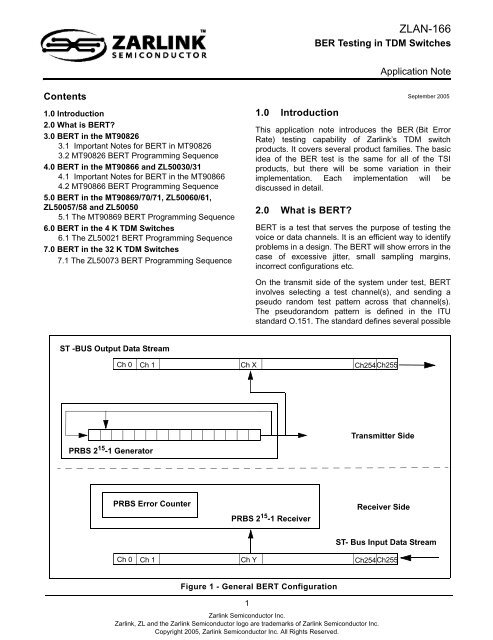
ST -BUS Output Data Stream<br />
PRBS 2 15 -1 Generator<br />
1<br />
1.0 Introduction<br />
This application note <strong>in</strong>troduces the <strong>BER</strong> (Bit Error<br />
Rate) test<strong>in</strong>g capability of Zarl<strong>in</strong>k’s <strong>TDM</strong> switch<br />
products. It covers several product families. The basic<br />
idea of the <strong>BER</strong> test is the same for all of the TSI<br />
products, but there will be some variation <strong>in</strong> their<br />
implementation. Each implementation will be<br />
discussed <strong>in</strong> detail.<br />
2.0 What is <strong>BER</strong>T?<br />
<strong>BER</strong>T is a test that serves the purpose of test<strong>in</strong>g the<br />
voice or data channels. It is an efficient way to identify<br />
problems <strong>in</strong> a design. The <strong>BER</strong>T will show errors <strong>in</strong> the<br />
case of excessive jitter, small sampl<strong>in</strong>g marg<strong>in</strong>s,<br />
<strong>in</strong>correct configurations etc.<br />
On the transmit side of the system under test, <strong>BER</strong>T<br />
<strong>in</strong>volves select<strong>in</strong>g a test channel(s), and send<strong>in</strong>g a<br />
pseudo random test pattern across that channel(s).<br />
The pseudorandom pattern is def<strong>in</strong>ed <strong>in</strong> the ITU<br />
standard O.151. The standard def<strong>in</strong>es several possible<br />
Figure 1 - General <strong>BER</strong>T Configuration<br />
Zarl<strong>in</strong>k <strong>Semiconductor</strong> Inc.<br />
Zarl<strong>in</strong>k, ZL and the Zarl<strong>in</strong>k <strong>Semiconductor</strong> logo are trademarks of Zarl<strong>in</strong>k <strong>Semiconductor</strong> Inc.<br />
Copyright 2005, Zarl<strong>in</strong>k <strong>Semiconductor</strong> Inc. All Rights Reserved.<br />
<strong>ZLAN</strong>-<strong>166</strong><br />
<strong>BER</strong> <strong>Test<strong>in</strong>g</strong> <strong>in</strong> <strong>TDM</strong> <strong>Switches</strong><br />
Ch 0 Ch 1 Ch X Ch254Ch255<br />
PRBS Error Counter<br />
PRBS 2 15 -1 Receiver<br />
Ch 0 Ch 1 Ch Y Ch254Ch255<br />
Application Note<br />
Transmitter Side<br />
Receiver Side<br />
September 2005<br />
ST- Bus Input Data Stream
<strong>ZLAN</strong>-<strong>166</strong> Application Note<br />
pseudorandom patterns but the most commonly used is the sequence of 2 15 -1. This sequence has a bit length of<br />
32767. It is constantly repeated dur<strong>in</strong>g the transmission of the <strong>BER</strong> test. This pattern is used <strong>in</strong> all of the devices<br />
discussed <strong>in</strong> this application note. Another pattern def<strong>in</strong>ed <strong>in</strong> O.151, implemented <strong>in</strong> one of the devices <strong>in</strong> this<br />
application note, is 2 23 -1.<br />
On the receiver side, after the pseudorandom pattern is received, it is recognized and the bit errors are detected<br />
and reported <strong>in</strong> the bit error rate counter. The variations between different <strong>BER</strong> implementations may <strong>in</strong>clude,<br />
<strong>BER</strong>T that spans across several channels, or several <strong>BER</strong>T transmitters and receivers per device.<br />
3.0 <strong>BER</strong>T <strong>in</strong> the MT90826<br />
The MT90826 allows users to perform bit error rate monitor<strong>in</strong>g by send<strong>in</strong>g a pseudo random pattern to a selected<br />
ST-BUS output channel and receiv<strong>in</strong>g that pattern from a selected ST-BUS <strong>in</strong>put channel. The pseudo random<br />
pattern is <strong>in</strong>ternally generated by the device with the 2 15 -1 polynomial.<br />
Users can select a pseudorandom pattern to be presented on a ST-BUS channel by programm<strong>in</strong>g the TM0 and<br />
TM1 bits <strong>in</strong> the connection memory. When TM0 and TM1 bits are high, the pseudorandom pattern is output on the<br />
selected ST-BUS output channel. The pseudo random pattern is then received by a ST-BUS <strong>in</strong>put channel which is<br />
selected us<strong>in</strong>g the BSA and BCA bits <strong>in</strong> the Bit Error Rate Input Selection Register - BISR(0x0011). An <strong>in</strong>ternal bit<br />
error counter keeps track of the error counts which is then stored <strong>in</strong> the Bit Error Count Register - BECR(0x0012).<br />
The bit error test is enabled and disabled by the S<strong>BER</strong> (bit 9) <strong>in</strong> the Control Register(0x0000). Sett<strong>in</strong>g the bit from<br />
zero to one <strong>in</strong>itiates the bit error test and enables the <strong>in</strong>ternal bit error counter. When the bit is programmed from<br />
one to zero, the device stops the bit error rate test and the <strong>in</strong>ternal bit error counter and transfers the error counts to<br />
the count register. A zero to one transition of the C<strong>BER</strong> (bit 10) of the Control Register (0x0000) resets the bit error<br />
count register and error counter.<br />
3.1 Important Notes for <strong>BER</strong>T <strong>in</strong> MT90826<br />
There are a few important notes about the MT90826 <strong>BER</strong>T test listed below:<br />
1. The <strong>BER</strong>T must be enabled on a s<strong>in</strong>gle only transmit channel and on one receive channel at any po<strong>in</strong>t <strong>in</strong> time. If<br />
the user mistakenly enables <strong>BER</strong> on several transmit ST- BUS channels, the <strong>BER</strong>T test will fail, because the<br />
<strong>BER</strong> polynomial will be split across all of the enabled channels, and one s<strong>in</strong>gle receive channel will thus receive<br />
<strong>in</strong>correct sequence.<br />
2. The MT90826 <strong>BER</strong>T implementation doesn’t have a lock <strong>in</strong>dication on the receive side. Therefore, the programmer<br />
may not know whether the <strong>BER</strong>T errors are occurr<strong>in</strong>g because the sequence is not locked or because there<br />
is someth<strong>in</strong>g wrong with the transmission channel. Therefore, the user must follow a specific programm<strong>in</strong>g<br />
sequence. The transmitter automatically starts transmitt<strong>in</strong>g when the output is enabled, the receiver will start<br />
receiv<strong>in</strong>g once the S<strong>BER</strong>(bit 9) of the Control Register (0x0000) is set. In all cases, the transmitter must be<br />
started before the receiver is enabled. If there is a significant delay <strong>in</strong> the system, it should be added between<br />
enabl<strong>in</strong>g of the transmitter and the receiver. If there is no significant delay <strong>in</strong> the system, the receiver can be<br />
enabled a couple of milliseconds after the transmitter. Before the lock has been achieved, there will be a constant<br />
number of bit errors counted <strong>in</strong> the bit error rate counter. The <strong>BER</strong> counter must be cleared before the<br />
actual test is started.<br />
3. The MT90826 does not recognize an <strong>in</strong>put of all ones as an error. If all ones are be<strong>in</strong>g sent to the <strong>in</strong>put channel,<br />
the <strong>BER</strong> counter does not <strong>in</strong>crement. Therefore, def<strong>in</strong>ed data should be sent to an <strong>in</strong>put channel by us<strong>in</strong>g a<br />
message mode to ensure proper connectivity, and then runn<strong>in</strong>g the <strong>BER</strong> test normally.<br />
4. After the power up, the content of the connection and the data memories is unknown. In order to ensure that the<br />
<strong>BER</strong>T is enabled on only one channel when the <strong>BER</strong>T test is started, the user must program the connection<br />
memory to a known value. The easiest way to program the connection memory is through block programm<strong>in</strong>g.<br />
All of the channels <strong>in</strong> the memory should be put to a non <strong>BER</strong> mode, for example, the message mode or tristate.<br />
2<br />
Zarl<strong>in</strong>k <strong>Semiconductor</strong> Inc.
3.2 MT90826 <strong>BER</strong>T Programm<strong>in</strong>g Sequence<br />
<strong>ZLAN</strong>-<strong>166</strong> Application Note<br />
The programm<strong>in</strong>g sequence for start<strong>in</strong>g a <strong>BER</strong>T on channel 1, stream 0 and receiv<strong>in</strong>g it on channel 5, stream 2 is<br />
shown below. It is assumed that there is an external connection between the stream 0 and stream 2 and that<br />
external to the device channel 1, stream 0 is switched to channel 5 stream 2. One such connection can be<br />
established through another TSI device, <strong>BER</strong>T may be tested if there is a physical loopback from one stream to<br />
another.<br />
The sequence is:<br />
1. Enable ODE<br />
2. Initialize the connection memory to message mode or tristate. The easiest way<br />
is to use connection memory block programm<strong>in</strong>g.<br />
3. Program the connection memory at 0x2001 with 0xE000. This step selects and<br />
enables the <strong>BER</strong> pattern for selected transmit channel.<br />
4. Wait a couple of milliseconds (or more depend<strong>in</strong>g on the external delay between<br />
the transmitter and the receiver). This wait is for the data to be looped<br />
from the transmitter to the receiver.<br />
5 Write 0x0205 to the BISR register (0x0011). This step selects the receive<br />
channel for a <strong>BER</strong> pattern.<br />
6. Clear the error counter by sett<strong>in</strong>g C<strong>BER</strong> bit (bit 10) of the Control Register<br />
(at address 0x0000) and clear<strong>in</strong>g it. This step is needed to clear any <strong>in</strong>itial<br />
errors that might have appeared before the lock has been established.<br />
7. The <strong>BER</strong>T is enabled by sett<strong>in</strong>g bit 9(S<strong>BER</strong> bit) of the Control Register (at<br />
address 0x0000) to 1.<br />
8. Wait for X msec. This is the user programmed desired <strong>BER</strong>T runn<strong>in</strong>g time.<br />
9. Disable <strong>BER</strong>T by clear<strong>in</strong>g S<strong>BER</strong> (bit 9) of the Control Register(0x0000).<br />
10.Check the Bit Error Counter Register(at 0x0012) for bit errors.<br />
4.0 <strong>BER</strong>T <strong>in</strong> the MT90866 and ZL50030/31<br />
The <strong>BER</strong> 2 15 - 1 test pattern capability is available on the MT90866 and ZL50030/31 as well. The example below<br />
will focus on the MT90866, but the same programm<strong>in</strong>g sequence can be applied to the ZL50030 and<br />
ZL50031.There is one <strong>BER</strong>T test feature for the backplane streams and one for the local streams. Those two tests<br />
are fully <strong>in</strong>dependent and can be runn<strong>in</strong>g at the same time.<br />
For the test, the transmitter and receiver portion of the <strong>BER</strong>T need to be configured. The transmitter is configured<br />
when the output channel and stream are programmed through the backplane or local connection memory. The<br />
receiver is programmed when the <strong>in</strong>put channel and stream are configured through the Local or Backplane <strong>BER</strong><br />
Input Selection (BIS) registers.<br />
4.1 Important Notes for <strong>BER</strong>T <strong>in</strong> the MT90866<br />
There are few important notes about the MT90866 <strong>BER</strong>T test listed below:<br />
1. For backplane or local streams the <strong>BER</strong>T must be enabled on only one transmit channel and on one receiver<br />
channel. For the backplane side, there can be only one backplane transmit channel and one receive channel<br />
runn<strong>in</strong>g <strong>BER</strong>T. The same applies for the local side. There can be only one <strong>BER</strong> test runn<strong>in</strong>g on the backplane<br />
and one <strong>BER</strong> test runn<strong>in</strong>g on the local side simultaneously.<br />
3<br />
Zarl<strong>in</strong>k <strong>Semiconductor</strong> Inc.
<strong>ZLAN</strong>-<strong>166</strong> Application Note<br />
If for any reason, the user enables <strong>BER</strong> on several transmit ST- BUS channels on the same side(either local or<br />
backplane), the <strong>BER</strong>T test will fail, because the <strong>BER</strong> polynomial will be split accross all of the enabled channels on<br />
one side, and the receiver will not be able to synchronize to the correct pattern.<br />
2. The MT90866 <strong>BER</strong>T implementation doesn’t have a lock <strong>in</strong>dication. Initially the user will not be able to determ<strong>in</strong>e<br />
if <strong>BER</strong> errors appear because of the sequence is not locked or because there is someth<strong>in</strong>g wrong with the<br />
transmission channel. Therefore, a specific programm<strong>in</strong>g sequence must be followed. The transmitter automatically<br />
starts transmitt<strong>in</strong>g when the output is enabled and the receiver will start receiv<strong>in</strong>g once the S<strong>BER</strong>B(or<br />
S<strong>BER</strong>L for the local side) bit <strong>in</strong> the Control Register(0x0000) is set. So, <strong>in</strong> all cases, the transmitter must be<br />
started before the receiver is enabled. If there is a significant delay <strong>in</strong> the system, this delay must be taken <strong>in</strong>to<br />
consideration and added to the programm<strong>in</strong>g sequence before the receiver is enabled. If there is no significant<br />
delay <strong>in</strong> the system, the receiver can be enabled a couple of milliseconds after the transmitter.<br />
Before the lock has been achieved, a few bit errors may appear <strong>in</strong> the bit error rate counter. The <strong>BER</strong> counter must<br />
be cleared before the actual test can be started.<br />
3. After a power up, the content of the connection and data memories is unknown. To ensure that the <strong>BER</strong>T is<br />
enabled on only one channel of the local or connection memory, before the <strong>BER</strong>T test is started, the user must<br />
program all the target connection memory to a known value. The easiest way to do this is through block programm<strong>in</strong>g,<br />
when all channels <strong>in</strong> the memory should be put to non <strong>BER</strong> mode, for example, the message mode,<br />
or tristate.<br />
4.2 MT90866 <strong>BER</strong>T Programm<strong>in</strong>g Sequence<br />
The programm<strong>in</strong>g sequence for start<strong>in</strong>g a <strong>BER</strong>T on transmit backplane channel 1, stream 0 and the receiver on<br />
backplane channel 5, stream 2 is shown below. It is assumed that there is an external connection between stream<br />
0 and stream 2 and that external to the device, channel 1, stream 0 is switched to channel 5 stream 2. One such<br />
connection can be established through another TSI. <strong>BER</strong>T can also be tested if there is a physical loopback from<br />
STo stream to STi streams. The same sequence can be used for programm<strong>in</strong>g <strong>BER</strong>T on local side when the<br />
correspond<strong>in</strong>g registers/bits are used.<br />
The sequence is:<br />
1. Enable ODE<br />
2. Initialize the backplane connection memory to message mode or tristate. The<br />
easiest way is to use the backplane connection memory block programm<strong>in</strong>g. This<br />
step is important to ensure that there are no channels of the backplane side<br />
that are <strong>in</strong> the <strong>BER</strong> mode before start<strong>in</strong>g the test.<br />
3. Program the backplane connection memory at 0x2001 with 0xE000. This step<br />
programs the backplane transmit stream 0, channel 1 for <strong>BER</strong> pattern. It also<br />
enables the backplane <strong>BER</strong> pattern on that channel.<br />
4. Wait a couple of milliseconds (or more depend<strong>in</strong>g on the external delay between<br />
the transmitter and the receiver). This wait for the transmit data to be<br />
looped back to receive side.<br />
5. Write 0x0205 to Backplane <strong>BER</strong> Input Selection Register - BBIS(0x0021). This<br />
step selects the backplane receive channel for <strong>BER</strong> pattern.<br />
6. The <strong>BER</strong>T is enabled on the receive side by sett<strong>in</strong>g S<strong>BER</strong>B(bit 7) of the Control<br />
Register (0x0000) to 1.<br />
7. Clear the error counter by sett<strong>in</strong>g C<strong>BER</strong>B bit (bit 8) of the Control Register<br />
(at address 0x0000) and clear<strong>in</strong>g it. This step is needed to clear any <strong>in</strong>itial<br />
errors that might have appeared before lock has been established.<br />
8. Wait for X msec. This is user programmed desired <strong>BER</strong>T runn<strong>in</strong>g time.<br />
9. Disable the backplane <strong>BER</strong>T by clear<strong>in</strong>g S<strong>BER</strong>B (bit 7) of the Control Register(at<br />
address 0x0000).<br />
4<br />
Zarl<strong>in</strong>k <strong>Semiconductor</strong> Inc.
<strong>ZLAN</strong>-<strong>166</strong> Application Note<br />
10. Check the Backplane Bit Error Counter Register(at 0x0029) for bit errors.<br />
Step 10 can also be performed before step 9 while the <strong>BER</strong>T is runn<strong>in</strong>g <strong>in</strong> order to dynamically check for errors.<br />
5.0 <strong>BER</strong>T <strong>in</strong> the MT90869/70/71, ZL50060/61, ZL50057/58 and ZL50050<br />
The <strong>BER</strong>T implementation is very similar <strong>in</strong> the MT90869/70/71 and the ZL50060/61(ZL50057/58 and ZL50050).<br />
Therefore, the details of the programm<strong>in</strong>g and description of the functionalities will be presented on the<br />
example of the MT90869. The only difference for ZL50060/61 (ZL50057/58 and ZL50050) devices, is the <strong>BER</strong>T<br />
test must be conducted offl<strong>in</strong>e, i.e the switch cannot pass traffic when the <strong>BER</strong>T is runn<strong>in</strong>g.<br />
Two separate <strong>BER</strong> test mechanisms are provided for the Local and Backplane ports. In both ports there is a <strong>BER</strong><br />
transmitter and a <strong>BER</strong> receiver. The transmitter generates a 2 15 -1 or 2 23 -1 Pseudo Random B<strong>in</strong>ary Sequence<br />
(PRBS), which may be allocated to a specific stream and a number of channels. This is def<strong>in</strong>ed by a stream<br />
number, a start channel number, and the number of consecutive channels follow<strong>in</strong>g the start channel.The stream,<br />
channel number and the number of consecutive channels follow<strong>in</strong>g the start channel are similarly allocated for the<br />
receiver. An example of the PRBS test is presented <strong>in</strong> the Figure 2. In this figure, the <strong>BER</strong>T is enabled on channels<br />
one, two and three of the selected stream - for example stream 0. Also, an assumption is made that the backplane<br />
stream 0 is physically looped back to backplane stream 2.<br />
Ch 0 Ch 1 Ch 2 Ch 3<br />
Ch254 Ch255<br />
Backplane<br />
Transmit<br />
Stream-BSTo<br />
(Example -stream 0)<br />
Backplane PRBS Generator<br />
BP PRBS Error Counter<br />
Backplane<br />
Receive<br />
Stream-BSTi<br />
(Example - stream 2)<br />
Ch 0 Ch 1 Ch251 Ch252Ch253<br />
Ch254 Ch255<br />
Backplane PRBS Receiver<br />
Local PRBS Generator<br />
Figure 2 - MT90869 <strong>BER</strong>T Implementation<br />
For the local side, the <strong>BER</strong>T is enabled on 5 consecutive transmit channels, channel 251 through channel 255 on<br />
transmit stream 5. On the receive local side, the match<strong>in</strong>g number of channels need to be programmed. But this<br />
time, we’ve chosen receive channels 10 through 14 of stream 4. This k<strong>in</strong>d of connection is possible only if the<br />
channels are externally switched us<strong>in</strong>g another TSI device which will switch transmit channels 251-255 of stream 5<br />
to receive channels 10 to 14 of stream 4.<br />
5<br />
Zarl<strong>in</strong>k <strong>Semiconductor</strong> Inc.<br />
Lcl PRBS Error Counter<br />
Ch 0 Ch 1 Ch 2 Ch 3<br />
Ch254 Ch255<br />
Local PRBS Receiver<br />
Local<br />
Transmit<br />
Stream-DSTo<br />
(Example-stream 5)<br />
Local<br />
Receive<br />
Stream-DSTi<br />
(Example-stream 4)<br />
Ch 0 Ch 1 Ch10 Ch11 Ch12 Ch13 Ch14<br />
Ch254Ch255
<strong>ZLAN</strong>-<strong>166</strong> Application Note<br />
When enabled, the receiver attempts to lock to the PRBS on the <strong>in</strong>com<strong>in</strong>g bit stream. Once the lock is achieved, by<br />
detection of a seed value, a bit by bit comparison takes place and each error <strong>in</strong>crements a 16-bit counter.The lock<br />
is <strong>in</strong>dicated by lock bits LOCKL for the local side and LOCKB for the backplane side. For MT90869/70/71 the<br />
counter will roll-over <strong>in</strong> the event of an error count <strong>in</strong> excess of 65535 decimal (0xFFFF). For ZL50060/61,<br />
ZL50057/58 and ZL50050, the <strong>BER</strong> counter will saturate.<br />
5.1 The MT90869 <strong>BER</strong>T Programm<strong>in</strong>g Sequence<br />
A programm<strong>in</strong>g example for sett<strong>in</strong>g up the backplane <strong>BER</strong>T test as shown <strong>in</strong> Figure 2 is described <strong>in</strong> this section.<br />
The same steps should be followed for runn<strong>in</strong>g the <strong>BER</strong>T on the local side.<br />
1. Enable ODE<br />
2. Program the Backplane <strong>BER</strong> Start Send Register - BBSSR (0x00C8)with desired<br />
backplane stream and start channel for <strong>BER</strong>T sequence. For the backplane<br />
stream 0 from Figure 2, the content should be 0x0001.<br />
3. The register Backplane Transmit <strong>BER</strong> Length Register - BTxBLR (0x00C9)conta<strong>in</strong>s<br />
the number of consecutive transmit channels that follow the start channel and<br />
that conta<strong>in</strong> the transmit PRBS sequence. For the backplane example from figure<br />
2, the content of the BTxBLR should be 0x0002.<br />
4. Program the Backplane <strong>BER</strong> Start Receive Register - BBSRR(0x00CB)with desired<br />
receive backplane stream and start channel for <strong>BER</strong>T sequence. For backplane<br />
receive channels from Figure 2, the content should be 0x0401.<br />
5. The Backplane Receive <strong>BER</strong> Length Register - BRXBLR (0x00CA)conta<strong>in</strong>s the number<br />
of consecutive receive channels that follow the start channel and receive the<br />
PRBS sequence. For this example, the content of the BRXBLR should be 0x0002.<br />
6. The backplane <strong>BER</strong> counter should be cleared before start<strong>in</strong>g the test. This is<br />
achieved by sett<strong>in</strong>g C<strong>BER</strong>B (bit 9) of the Bit Error Rate Test Control Register -<br />
<strong>BER</strong>CR (0x0002).<br />
7. The desired backplane <strong>BER</strong> pattern should be chosen through PRBSB(bit 6) of the<br />
<strong>BER</strong>CR(0x0002). For 2 15 -1 sequence, this bit should be programmed to 0.<br />
8. The <strong>BER</strong>T test is started by sett<strong>in</strong>g S<strong>BER</strong>RXB(bit 8) and S<strong>BER</strong>TXB(bit 7) of the<br />
<strong>BER</strong>CR register (0x0002). The order of sett<strong>in</strong>g these two bits is not important.<br />
9. Wait for the backplane <strong>BER</strong>T lock <strong>in</strong>dication. This is done by monitor<strong>in</strong>g bit<br />
LOCKB(bit 11). If this bit is one the backplane <strong>BER</strong>T receiver has locked.<br />
10. Wait for X msec. This is user programmed desired <strong>BER</strong>T runn<strong>in</strong>g time.<br />
11. The <strong>BER</strong>T test is stopped by programm<strong>in</strong>g bits S<strong>BER</strong>RXB(bit 8)and S<strong>BER</strong>TXB(bit 7)<br />
to 0.<br />
12. Read the number of errors from <strong>BER</strong> counter - BBCR register(0x00CC).<br />
6.0 <strong>BER</strong>T <strong>in</strong> the 4 K <strong>TDM</strong> <strong>Switches</strong><br />
The 4 K <strong>TDM</strong> switch portfolio consists of several devices rang<strong>in</strong>g from the ZL50015 to ZL50023. The <strong>BER</strong>T will be<br />
expla<strong>in</strong>ed on the example of the ZL50021 device, the most feature rich 4 K device. A similar test can be easily<br />
applied to the other 4 K devices.<br />
The ZL50021 has one <strong>BER</strong> transmitter and one <strong>BER</strong> receiver for each pair of the <strong>in</strong>put and the output streams,<br />
result<strong>in</strong>g <strong>in</strong> the 32 transmitters connected to the output streams and 32 receivers associated with the <strong>in</strong>put streams.<br />
Each transmitter can generate a <strong>BER</strong> sequence with a pattern of 2 15 -1 pseudorandom code (ITU O.151). Each<br />
transmitter can start at any location on the stream and will last for a m<strong>in</strong>imum of 1 channel to a maximum of 1 frame<br />
(125 µs). The global <strong>BER</strong> enable bits R<strong>BER</strong>EN (bit 5) and T<strong>BER</strong>EN (bit 4) <strong>in</strong> the IMS register should be<br />
programmed before the <strong>BER</strong> is started. In order to save power, the 32 transmitters and/or receivers can be<br />
6<br />
Zarl<strong>in</strong>k <strong>Semiconductor</strong> Inc.
<strong>ZLAN</strong>-<strong>166</strong> Application Note<br />
disabled. Multiple connection memory locations can be programmed for <strong>BER</strong> tests, such that the <strong>BER</strong> patterns can<br />
be transmitted for multiple consecutive output channels. If consecutive <strong>in</strong>put channels are not selected, the <strong>BER</strong><br />
receiver will not correctly compare the bit patterns. The number of output channels which the <strong>BER</strong> pattern occupies<br />
has to be the same as the number of channels def<strong>in</strong>ed <strong>in</strong> the <strong>BER</strong> Length Register (BRLR) which def<strong>in</strong>es how<br />
many <strong>BER</strong> channels are to be monitor by the <strong>BER</strong> receiver. When the lock has been detected the lock <strong>in</strong>dication<br />
bits <strong>in</strong> the <strong>BER</strong> receiver LOCK register will be set.<br />
Transmit stream STo0<br />
Ch 0 Ch 1 Ch 2 Ch 3<br />
Ch254 Ch255<br />
PRBS Generator 0<br />
PRBS Error Counter 0<br />
Transmit stream STo31<br />
Ch 0 Ch 1 Ch251 Ch252Ch253<br />
Ch254 Ch255<br />
PRBS Receiver 0<br />
Ch 0 Ch 1<br />
6.1 The ZL50021 <strong>BER</strong>T Programm<strong>in</strong>g Sequence<br />
The ZL50021 programm<strong>in</strong>g sequence is as follows:<br />
PRBS Generator 31<br />
Figure 3 - ZL50021 <strong>BER</strong>T Implementation<br />
1.Enable ODE<br />
2.Initialize the connection memory to message mode or tristate. The easiest way is<br />
to use the connection memory block programm<strong>in</strong>g. This step is important to<br />
ensure that there are no channels that are <strong>in</strong> the <strong>BER</strong> mode before start<strong>in</strong>g the<br />
test.<br />
3. Program the T<strong>BER</strong>EN (bit 4) and R<strong>BER</strong>EN (bit 5) <strong>in</strong> the IMS(0x0001) register to<br />
enable all transmitters and receivers.<br />
4. Program the desired channels <strong>in</strong> the connection memory to send the <strong>BER</strong>T. For<br />
the <strong>BER</strong>T to run, the CMM(bit 0) of the connection memory low must be 1. Also,<br />
bits PCC1-0(bits 2-1) must be 10 to enable the per stream <strong>BER</strong> transmitters.<br />
For the backplane example of figure 3, the connection memory addresses<br />
0x2001,0x2003 and 0x2003 should be programmed with 0x0005.<br />
7<br />
PRBS Error Counter 31<br />
Ch 0 Ch 1 Ch 2 Ch 3<br />
Ch254 Ch255<br />
Zarl<strong>in</strong>k <strong>Semiconductor</strong> Inc.<br />
PRBS Receiver 31<br />
Receive stream STi31<br />
Ch251 Ch252Ch253<br />
Ch254 Ch255<br />
Receive stream STi0
<strong>ZLAN</strong>-<strong>166</strong> Application Note<br />
5. Before enabl<strong>in</strong>g the transmitter and the receiver there must be a m<strong>in</strong>imum two<br />
frame wait.If there is significant delay between transmitter and the receiver,<br />
that delay should be added to this wait.<br />
6. Program a start channel <strong>in</strong> the receiver from which the <strong>BER</strong> receive test is<br />
start<strong>in</strong>g to be monitored. This is done by writ<strong>in</strong>g to <strong>BER</strong> Receiver Start<br />
Register N - BRSR(n)(0x0300-0x031F).For the stream 0 example from figure 3,<br />
0x0001 should be written to BRSR0(0x0300) There is one register for each<br />
receive stream.<br />
7. The <strong>BER</strong> Receiver Length Registers BRLRn(0x0320 - 0x033F)conta<strong>in</strong> the number of<br />
consecutive receive channels that are receiv<strong>in</strong>g the <strong>BER</strong> pattern per stream.<br />
The m<strong>in</strong>imum number of channels that conta<strong>in</strong> <strong>BER</strong>T is one and the maximum number<br />
is the number of channels <strong>in</strong> a frame. On the example of the receive stream 0,<br />
there are three channels, receiv<strong>in</strong>g the <strong>BER</strong> pattern and therefore the content<br />
of the BRLR0 should be 0x0003.<br />
8. The <strong>BER</strong>T test is actually started by programm<strong>in</strong>g S<strong>BER</strong>(bit 0) of the <strong>BER</strong><br />
Receiver Control Register BRCRn (0x0340 - 0x035F) for the desired stream.<br />
9. Wait for <strong>BER</strong>T lock <strong>in</strong>dication. This is done by monitor<strong>in</strong>g the correspond<strong>in</strong>g<br />
bit of the <strong>BER</strong> Receiver Lock Registers 0 and 1 - <strong>BER</strong>LR0(0x0013) and<br />
<strong>BER</strong>LR1(0x0014).<br />
10.Clear the <strong>BER</strong>T counters. This is achieved by sett<strong>in</strong>g the C<strong>BER</strong> bit(bit 1)of the<br />
<strong>BER</strong> Control Registers - BRCRn (0x0340 - 0x035F) for the desired stream.<br />
11.Wait for X msec. This is the user programmed desired <strong>BER</strong>T runn<strong>in</strong>g time.<br />
12.The <strong>BER</strong>T test is stopped by programm<strong>in</strong>g bit S<strong>BER</strong>(bit 0)of the BRCRn register to<br />
0.<br />
13.Read the number of errors from <strong>BER</strong> counter. There is one counter for each <strong>BER</strong><br />
rate receiver for a total of 32 counters. The counters can be read from BRERn<br />
registers(0x0360 - 0x037F).<br />
7.0 <strong>BER</strong>T <strong>in</strong> the 32 K <strong>TDM</strong> <strong>Switches</strong><br />
The 32 K <strong>TDM</strong> switch portfolio consists of several devices <strong>in</strong>clud<strong>in</strong>g the ZL50070, ZL50073, ZL50074 and<br />
ZL50075. The <strong>BER</strong>T will be expla<strong>in</strong>ed on the example of the ZL50073 device, the most feature rich device. A<br />
similar test can be easily applied to other 32 K devices with the exception of the ZL50074 which doesn’t support<br />
<strong>BER</strong>T capability.<br />
There are 128 transmit streams and 128 receive streams <strong>in</strong> the ZL50073. Each transmit STo stream has an<br />
associated <strong>BER</strong> transmitter and each receive STi stream has an associated <strong>BER</strong> receiver. Similar to the other<br />
devices described <strong>in</strong> this note, the <strong>BER</strong>T pattern used is 2 15 -1. For 8.192 Mbps and 16.384 Mbps modes, the<br />
maximum number of transmit and receive streams is 128(each). Therefore, the maximum number of <strong>BER</strong> tests that<br />
can be runn<strong>in</strong>g simultaneously is 128. For 32.768 Mbps the maximum number of <strong>BER</strong> tests simultaneously runn<strong>in</strong>g<br />
is 64 and for 65.536 Mbps, it is 32. There is one <strong>BER</strong> counter associated with each <strong>BER</strong> receiver which amounts to<br />
the maximum of 128, 64 or 32 <strong>BER</strong>T counters depend<strong>in</strong>g on the stream rate. When the counter is saturated to<br />
65535 it doesn’t rollover. It can be reset by reset<strong>in</strong>g the device or writ<strong>in</strong>g to the counter.<br />
The <strong>BER</strong> pattern can be enabled on a m<strong>in</strong>imum of one channel and a maximum of 1024 channels. The maximum<br />
number of channels depends on the stream rate, for the 65.536 Mbps, it is 1024, for the 32.768 Mbps it is 512, for<br />
16.384 Mbps it is 256 and for 8.192 Mbps, it is 128 channels. Unlike other <strong>BER</strong>T implementations described <strong>in</strong> this<br />
document, here we can enable <strong>BER</strong>T mode for channels that are not consecutive. It is important that transmit and<br />
receive channels are correspond<strong>in</strong>g and that the order <strong>in</strong> which the channels are sent is the same as the order <strong>in</strong><br />
which they are received.<br />
8<br />
Zarl<strong>in</strong>k <strong>Semiconductor</strong> Inc.
Figure 4 illustrates the <strong>BER</strong> test as implemented <strong>in</strong> the ZL50073 <strong>TDM</strong> switch.<br />
7.1 The ZL50073 <strong>BER</strong>T Programm<strong>in</strong>g Sequence<br />
<strong>ZLAN</strong>-<strong>166</strong> Application Note<br />
Transmit stream 0(SToA0)<br />
Ch 0 Ch 1 Ch 2 Ch 3<br />
Ch254 Ch255<br />
PRBS Generator 0<br />
PRBS Error Counter 0<br />
Transmit stream 127(SToD31)<br />
Ch 0 Ch 1 Ch251 Ch252Ch253<br />
Ch254 Ch255<br />
PRBS Receiver 0<br />
Ch 0 Ch 1<br />
PRBS Generator 127<br />
Figure 4 - ZL50073 <strong>BER</strong>T Implementation<br />
Based on the Figure 4 example for the stream SToA0 and STiA0, the ZL50073 programm<strong>in</strong>g sequence is as<br />
follows:<br />
1. Enable ODE<br />
2. Initialize the connection memory to message mode or tristate mode. The easiest<br />
way is to use the connection memory block programm<strong>in</strong>g. This step is important<br />
to ensure that there are no channels that are <strong>in</strong> the <strong>BER</strong> mode before start<strong>in</strong>g<br />
the test.<br />
3. For the example of STiA0 stream, channels 0,2 and 3, programPCF2-0(Bits 31-29)<br />
of the connection memory at addresses 0x00000,0x00008 and 0x0000C to<br />
0xA0000000. This step programs the transmit stream STiA0, channels 0,2 and 3<br />
for the <strong>BER</strong> pattern.It also enables the <strong>BER</strong> pattern on those channels.<br />
4. Wait a couple of ms (or more depend<strong>in</strong>g on the external delay between the<br />
transmitter and the receiver). This wait is needed for the transmit data to be<br />
looped back to receive side.<br />
9<br />
PRBS Error Counter 127<br />
Ch 0 Ch 1 Ch 2 Ch 3<br />
Ch254 Ch255<br />
Zarl<strong>in</strong>k <strong>Semiconductor</strong> Inc.<br />
PRBS Receiver 127<br />
Receive stream 127(STiD31)<br />
Ch251 Ch252Ch253<br />
Ch254 Ch255<br />
Receive stream 0 (STiA0)
<strong>ZLAN</strong>-<strong>166</strong> Application Note<br />
5. The receive stream and channel for the <strong>BER</strong> pattern is enabled by writ<strong>in</strong>g to the<br />
<strong>BER</strong> Enable Control Memory. For the full <strong>BER</strong> Enable Control Memory Address Map,<br />
please refer to ZL50073 datasheet, section 14.3.1. The start of <strong>BER</strong> Enable<br />
Control Memory is at address offset 0x030000. So, <strong>in</strong> order to enable the<br />
receiver on stream 0 to receive the <strong>BER</strong> pattern on channels 0,2 and 3,bit<br />
BCE(bit 0) <strong>in</strong> the <strong>BER</strong> Enable Control Memory Addresses, should be programmed to<br />
0x01000101 (for 32 bit access). Each byte of this 32 bit memory location<br />
corresponds to one of the first four channels of the stream 0.<br />
6. Before start<strong>in</strong>g the <strong>BER</strong> test, the correspond<strong>in</strong>g counter for the <strong>in</strong>put stream<br />
should be cleared.The counter is cleared by writ<strong>in</strong>g 0 to it.For the example, <strong>in</strong><br />
figure 4, for stream 0, 0 would be written to address 0x040000.<br />
7. Wait for X msec. This is the user programmed desired <strong>BER</strong>T runn<strong>in</strong>g time.<br />
8. Check the Bit Error Counter Register(0x040000 address offset for stream 0) for<br />
bit errors.<br />
9. Disable the <strong>BER</strong>T by programm<strong>in</strong>g the BCE bit of the <strong>BER</strong> Enable Control Memory<br />
Address for stream 0 to 0x0. As <strong>in</strong> step 5, the address location 0x030000 should<br />
be programmed with 0x0.<br />
10<br />
Zarl<strong>in</strong>k <strong>Semiconductor</strong> Inc.
www.zarl<strong>in</strong>k.com<br />
Information relat<strong>in</strong>g to products and services furnished here<strong>in</strong> by Zarl<strong>in</strong>k <strong>Semiconductor</strong> Inc. or its subsidiaries (collectively “Zarl<strong>in</strong>k”) is believed to be reliable.<br />
However, Zarl<strong>in</strong>k assumes no liability for errors that may appear <strong>in</strong> this publication, or for liability otherwise aris<strong>in</strong>g from the application or use of any such<br />
<strong>in</strong>formation, product or service or for any <strong>in</strong>fr<strong>in</strong>gement of patents or other <strong>in</strong>tellectual property rights owned by third parties which may result from such application or<br />
use. Neither the supply of such <strong>in</strong>formation or purchase of product or service conveys any license, either express or implied, under patents or other <strong>in</strong>tellectual<br />
property rights owned by Zarl<strong>in</strong>k or licensed from third parties by Zarl<strong>in</strong>k, whatsoever. Purchasers of products are also hereby notified that the use of product <strong>in</strong><br />
certa<strong>in</strong> ways or <strong>in</strong> comb<strong>in</strong>ation with Zarl<strong>in</strong>k, or non-Zarl<strong>in</strong>k furnished goods or services may <strong>in</strong>fr<strong>in</strong>ge patents or other <strong>in</strong>tellectual property rights owned by Zarl<strong>in</strong>k.<br />
This publication is issued to provide <strong>in</strong>formation only and (unless agreed by Zarl<strong>in</strong>k <strong>in</strong> writ<strong>in</strong>g) may not be used, applied or reproduced for any purpose nor form part<br />
of any order or contract nor to be regarded as a representation relat<strong>in</strong>g to the products or services concerned. The products, their specifications, services and other<br />
<strong>in</strong>formation appear<strong>in</strong>g <strong>in</strong> this publication are subject to change by Zarl<strong>in</strong>k without notice. No warranty or guarantee express or implied is made regard<strong>in</strong>g the<br />
capability, performance or suitability of any product or service. Information concern<strong>in</strong>g possible methods of use is provided as a guide only and does not constitute<br />
any guarantee that such methods of use will be satisfactory <strong>in</strong> a specific piece of equipment. It is the user’s responsibility to fully determ<strong>in</strong>e the performance and<br />
suitability of any equipment us<strong>in</strong>g such <strong>in</strong>formation and to ensure that any publication or data used is up to date and has not been superseded. Manufactur<strong>in</strong>g does<br />
not necessarily <strong>in</strong>clude test<strong>in</strong>g of all functions or parameters. These products are not suitable for use <strong>in</strong> any medical products whose failure to perform may result <strong>in</strong><br />
significant <strong>in</strong>jury or death to the user. All products and materials are sold and services provided subject to Zarl<strong>in</strong>k’s conditions of sale which are available on request.<br />
Purchase of Zarl<strong>in</strong>k’s I 2 C components conveys a licence under the Philips I 2 C Patent rights to use these components <strong>in</strong> and I 2 C System, provided that the system<br />
conforms to the I 2 C Standard Specification as def<strong>in</strong>ed by Philips.<br />
Zarl<strong>in</strong>k, ZL and the Zarl<strong>in</strong>k <strong>Semiconductor</strong> logo are trademarks of Zarl<strong>in</strong>k <strong>Semiconductor</strong> Inc.<br />
Copyright Zarl<strong>in</strong>k <strong>Semiconductor</strong> Inc. All Rights Reserved.<br />
For more <strong>in</strong>formation about all Zarl<strong>in</strong>k products<br />
visit our Web Site at<br />
TECHNICAL DOCUMENTATION - NOT FOR RESALE