ZLAN-166 BER Testing in TDM Switches.pdf - Zarlink Semiconductor
ZLAN-166 BER Testing in TDM Switches.pdf - Zarlink Semiconductor
ZLAN-166 BER Testing in TDM Switches.pdf - Zarlink Semiconductor

Create successful ePaper yourself
Turn your PDF publications into a flip-book with our unique Google optimized e-Paper software.
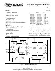
<strong>ZLAN</strong>-<strong>166</strong> Application Note<br />
If for any reason, the user enables <strong>BER</strong> on several transmit ST- BUS channels on the same side(either local or<br />
backplane), the <strong>BER</strong>T test will fail, because the <strong>BER</strong> polynomial will be split accross all of the enabled channels on<br />
one side, and the receiver will not be able to synchronize to the correct pattern.<br />
2. The MT90866 <strong>BER</strong>T implementation doesn’t have a lock <strong>in</strong>dication. Initially the user will not be able to determ<strong>in</strong>e<br />
if <strong>BER</strong> errors appear because of the sequence is not locked or because there is someth<strong>in</strong>g wrong with the<br />
transmission channel. Therefore, a specific programm<strong>in</strong>g sequence must be followed. The transmitter automatically<br />
starts transmitt<strong>in</strong>g when the output is enabled and the receiver will start receiv<strong>in</strong>g once the S<strong>BER</strong>B(or<br />
S<strong>BER</strong>L for the local side) bit <strong>in</strong> the Control Register(0x0000) is set. So, <strong>in</strong> all cases, the transmitter must be<br />
started before the receiver is enabled. If there is a significant delay <strong>in</strong> the system, this delay must be taken <strong>in</strong>to<br />
consideration and added to the programm<strong>in</strong>g sequence before the receiver is enabled. If there is no significant<br />
delay <strong>in</strong> the system, the receiver can be enabled a couple of milliseconds after the transmitter.<br />
Before the lock has been achieved, a few bit errors may appear <strong>in</strong> the bit error rate counter. The <strong>BER</strong> counter must<br />
be cleared before the actual test can be started.<br />
3. After a power up, the content of the connection and data memories is unknown. To ensure that the <strong>BER</strong>T is<br />
enabled on only one channel of the local or connection memory, before the <strong>BER</strong>T test is started, the user must<br />
program all the target connection memory to a known value. The easiest way to do this is through block programm<strong>in</strong>g,<br />
when all channels <strong>in</strong> the memory should be put to non <strong>BER</strong> mode, for example, the message mode,<br />
or tristate.<br />
4.2 MT90866 <strong>BER</strong>T Programm<strong>in</strong>g Sequence<br />
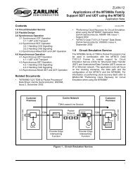
The programm<strong>in</strong>g sequence for start<strong>in</strong>g a <strong>BER</strong>T on transmit backplane channel 1, stream 0 and the receiver on<br />
backplane channel 5, stream 2 is shown below. It is assumed that there is an external connection between stream<br />
0 and stream 2 and that external to the device, channel 1, stream 0 is switched to channel 5 stream 2. One such<br />
connection can be established through another TSI. <strong>BER</strong>T can also be tested if there is a physical loopback from<br />
STo stream to STi streams. The same sequence can be used for programm<strong>in</strong>g <strong>BER</strong>T on local side when the<br />
correspond<strong>in</strong>g registers/bits are used.<br />
The sequence is:<br />
1. Enable ODE<br />
2. Initialize the backplane connection memory to message mode or tristate. The<br />
easiest way is to use the backplane connection memory block programm<strong>in</strong>g. This<br />
step is important to ensure that there are no channels of the backplane side<br />
that are <strong>in</strong> the <strong>BER</strong> mode before start<strong>in</strong>g the test.<br />
3. Program the backplane connection memory at 0x2001 with 0xE000. This step<br />
programs the backplane transmit stream 0, channel 1 for <strong>BER</strong> pattern. It also<br />
enables the backplane <strong>BER</strong> pattern on that channel.<br />
4. Wait a couple of milliseconds (or more depend<strong>in</strong>g on the external delay between<br />
the transmitter and the receiver). This wait for the transmit data to be<br />
looped back to receive side.<br />
5. Write 0x0205 to Backplane <strong>BER</strong> Input Selection Register - BBIS(0x0021). This<br />
step selects the backplane receive channel for <strong>BER</strong> pattern.<br />
6. The <strong>BER</strong>T is enabled on the receive side by sett<strong>in</strong>g S<strong>BER</strong>B(bit 7) of the Control<br />
Register (0x0000) to 1.<br />
7. Clear the error counter by sett<strong>in</strong>g C<strong>BER</strong>B bit (bit 8) of the Control Register<br />
(at address 0x0000) and clear<strong>in</strong>g it. This step is needed to clear any <strong>in</strong>itial<br />
errors that might have appeared before lock has been established.<br />
8. Wait for X msec. This is user programmed desired <strong>BER</strong>T runn<strong>in</strong>g time.<br />
9. Disable the backplane <strong>BER</strong>T by clear<strong>in</strong>g S<strong>BER</strong>B (bit 7) of the Control Register(at<br />
address 0x0000).<br />
4<br />
Zarl<strong>in</strong>k <strong>Semiconductor</strong> Inc.