ZLAN-166 BER Testing in TDM Switches.pdf - Zarlink Semiconductor
ZLAN-166 BER Testing in TDM Switches.pdf - Zarlink Semiconductor
ZLAN-166 BER Testing in TDM Switches.pdf - Zarlink Semiconductor

Create successful ePaper yourself
Turn your PDF publications into a flip-book with our unique Google optimized e-Paper software.
Figure 4 illustrates the <strong>BER</strong> test as implemented <strong>in</strong> the ZL50073 <strong>TDM</strong> switch.<br />
7.1 The ZL50073 <strong>BER</strong>T Programm<strong>in</strong>g Sequence<br />
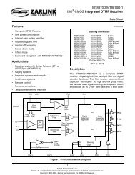
<strong>ZLAN</strong>-<strong>166</strong> Application Note<br />
Transmit stream 0(SToA0)<br />
Ch 0 Ch 1 Ch 2 Ch 3<br />
Ch254 Ch255<br />
PRBS Generator 0<br />
PRBS Error Counter 0<br />
Transmit stream 127(SToD31)<br />
Ch 0 Ch 1 Ch251 Ch252Ch253<br />
Ch254 Ch255<br />
PRBS Receiver 0<br />
Ch 0 Ch 1<br />
PRBS Generator 127<br />
Figure 4 - ZL50073 <strong>BER</strong>T Implementation<br />
Based on the Figure 4 example for the stream SToA0 and STiA0, the ZL50073 programm<strong>in</strong>g sequence is as<br />
follows:<br />
1. Enable ODE<br />
2. Initialize the connection memory to message mode or tristate mode. The easiest<br />
way is to use the connection memory block programm<strong>in</strong>g. This step is important<br />
to ensure that there are no channels that are <strong>in</strong> the <strong>BER</strong> mode before start<strong>in</strong>g<br />
the test.<br />
3. For the example of STiA0 stream, channels 0,2 and 3, programPCF2-0(Bits 31-29)<br />
of the connection memory at addresses 0x00000,0x00008 and 0x0000C to<br />
0xA0000000. This step programs the transmit stream STiA0, channels 0,2 and 3<br />
for the <strong>BER</strong> pattern.It also enables the <strong>BER</strong> pattern on those channels.<br />
4. Wait a couple of ms (or more depend<strong>in</strong>g on the external delay between the<br />
transmitter and the receiver). This wait is needed for the transmit data to be<br />
looped back to receive side.<br />
9<br />
PRBS Error Counter 127<br />
Ch 0 Ch 1 Ch 2 Ch 3<br />
Ch254 Ch255<br />
Zarl<strong>in</strong>k <strong>Semiconductor</strong> Inc.<br />
PRBS Receiver 127<br />
Receive stream 127(STiD31)<br />
Ch251 Ch252Ch253<br />
Ch254 Ch255<br />
Receive stream 0 (STiA0)