ZLAN-166 BER Testing in TDM Switches.pdf - Zarlink Semiconductor
ZLAN-166 BER Testing in TDM Switches.pdf - Zarlink Semiconductor
ZLAN-166 BER Testing in TDM Switches.pdf - Zarlink Semiconductor

Create successful ePaper yourself
Turn your PDF publications into a flip-book with our unique Google optimized e-Paper software.
<strong>ZLAN</strong>-<strong>166</strong> Application Note<br />
disabled. Multiple connection memory locations can be programmed for <strong>BER</strong> tests, such that the <strong>BER</strong> patterns can<br />
be transmitted for multiple consecutive output channels. If consecutive <strong>in</strong>put channels are not selected, the <strong>BER</strong><br />
receiver will not correctly compare the bit patterns. The number of output channels which the <strong>BER</strong> pattern occupies<br />
has to be the same as the number of channels def<strong>in</strong>ed <strong>in</strong> the <strong>BER</strong> Length Register (BRLR) which def<strong>in</strong>es how<br />
many <strong>BER</strong> channels are to be monitor by the <strong>BER</strong> receiver. When the lock has been detected the lock <strong>in</strong>dication<br />
bits <strong>in</strong> the <strong>BER</strong> receiver LOCK register will be set.<br />
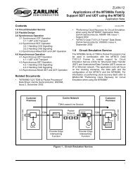
Transmit stream STo0<br />
Ch 0 Ch 1 Ch 2 Ch 3<br />
Ch254 Ch255<br />
PRBS Generator 0<br />
PRBS Error Counter 0<br />
Transmit stream STo31<br />
Ch 0 Ch 1 Ch251 Ch252Ch253<br />
Ch254 Ch255<br />
PRBS Receiver 0<br />
Ch 0 Ch 1<br />
6.1 The ZL50021 <strong>BER</strong>T Programm<strong>in</strong>g Sequence<br />
The ZL50021 programm<strong>in</strong>g sequence is as follows:<br />
PRBS Generator 31<br />
Figure 3 - ZL50021 <strong>BER</strong>T Implementation<br />
1.Enable ODE<br />
2.Initialize the connection memory to message mode or tristate. The easiest way is<br />
to use the connection memory block programm<strong>in</strong>g. This step is important to<br />
ensure that there are no channels that are <strong>in</strong> the <strong>BER</strong> mode before start<strong>in</strong>g the<br />
test.<br />
3. Program the T<strong>BER</strong>EN (bit 4) and R<strong>BER</strong>EN (bit 5) <strong>in</strong> the IMS(0x0001) register to<br />
enable all transmitters and receivers.<br />
4. Program the desired channels <strong>in</strong> the connection memory to send the <strong>BER</strong>T. For<br />
the <strong>BER</strong>T to run, the CMM(bit 0) of the connection memory low must be 1. Also,<br />
bits PCC1-0(bits 2-1) must be 10 to enable the per stream <strong>BER</strong> transmitters.<br />
For the backplane example of figure 3, the connection memory addresses<br />
0x2001,0x2003 and 0x2003 should be programmed with 0x0005.<br />
7<br />
PRBS Error Counter 31<br />
Ch 0 Ch 1 Ch 2 Ch 3<br />
Ch254 Ch255<br />
Zarl<strong>in</strong>k <strong>Semiconductor</strong> Inc.<br />
PRBS Receiver 31<br />
Receive stream STi31<br />
Ch251 Ch252Ch253<br />
Ch254 Ch255<br />
Receive stream STi0