MT8870DE1-1 - Zarlink Semiconductor
MT8870DE1-1 - Zarlink Semiconductor
MT8870DE1-1 - Zarlink Semiconductor

Create successful ePaper yourself
Turn your PDF publications into a flip-book with our unique Google optimized e-Paper software.
Features<br />
• Complete DTMF Receiver<br />
• Low power consumption<br />
• Internal gain setting amplifier<br />
• Adjustable guard time<br />
• Central office quality<br />
• Power-down mode<br />
• Inhibit mode<br />
• Backward compatible with MT8870C/MT8870C-1<br />
Applications<br />
• Receiver system for British Telecom (BT) or<br />
CEPT Spec (MT8870D-1)<br />
• Paging systems<br />
• Repeater systems/mobile radio<br />
• Credit card systems<br />
• Remote control<br />
• Personal computers<br />
• Telephone answering machine<br />
PWDN<br />
IN +<br />
IN -<br />
GS<br />
Chip<br />
Power<br />
1<br />
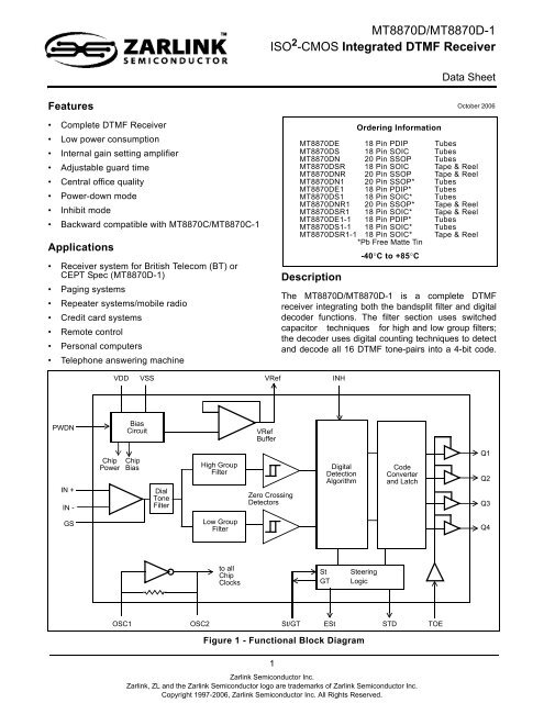
Description<br />
VDD VSS VRef INH<br />
Bias<br />
Circuit<br />
Chip<br />
Bias<br />
Dial<br />
Tone<br />
Filter<br />
High Group<br />
Filter<br />
Low Group<br />
Filter<br />
to all<br />
Chip<br />
Clocks<br />
VRef<br />
Buffer<br />
MT8870D/MT8870D-1<br />
ISO 2 -CMOS Integrated DTMF Receiver<br />
Zero Crossing<br />
Detectors<br />
Ordering Information<br />
The MT8870D/MT8870D-1 is a complete DTMF<br />
receiver integrating both the bandsplit filter and digital<br />
decoder functions. The filter section uses switched<br />
capacitor techniques for high and low group filters;<br />
the decoder uses digital counting techniques to detect<br />
and decode all 16 DTMF tone-pairs into a 4-bit code.<br />
Figure 1 - Functional Block Diagram<br />
<strong>Zarlink</strong> <strong>Semiconductor</strong> Inc.<br />
<strong>Zarlink</strong>, ZL and the <strong>Zarlink</strong> <strong>Semiconductor</strong> logo are trademarks of <strong>Zarlink</strong> <strong>Semiconductor</strong> Inc.<br />
Copyright 1997-2006, <strong>Zarlink</strong> <strong>Semiconductor</strong> Inc. All Rights Reserved.<br />
October 2006<br />
MT8870DE 18 Pin PDIP Tubes<br />
MT8870DS 18 Pin SOIC Tubes<br />
MT8870DN 20 Pin SSOP Tubes<br />
MT8870DSR 18 Pin SOIC Tape & Reel<br />
MT8870DNR 20 Pin SSOP Tape & Reel<br />
MT8870DN1 20 Pin SSOP* Tubes<br />
<strong>MT8870DE1</strong> 18 Pin PDIP* Tubes<br />
MT8870DS1 18 Pin SOIC* Tubes<br />
MT8870DNR1 20 Pin SSOP* Tape & Reel<br />
MT8870DSR1 18 Pin SOIC* Tape & Reel<br />
<strong>MT8870DE1</strong>-1 18 Pin PDIP* Tubes<br />
MT8870DS1-1 18 Pin SOIC* Tubes<br />
MT8870DSR1-1 18 Pin SOIC* Tape & Reel<br />
*Pb Free Matte Tin<br />
Digital<br />
Detection<br />
Algorithm<br />
-40°C to +85°C<br />
Code<br />
Converter<br />
and Latch<br />
OSC1 OSC2 St/GT ESt STD TOE<br />
St<br />
GT<br />
Steering<br />
Logic<br />
Data Sheet<br />
Q1<br />
Q2<br />
Q3<br />
Q4
MT8870D/MT8870D-1 Data Sheet<br />
External component count is minimized by on chip provision of a differential input amplifier, clock oscillator and<br />
latched three-state bus interface.<br />
Pin Description<br />
Pin #<br />
18 20<br />
IN+<br />
IN-<br />
GS<br />
VRef<br />
INH<br />
PWDN<br />
OSC1<br />
OSC2<br />
VSS<br />
1<br />
18<br />
2<br />
17<br />
3<br />
16<br />
4<br />
15<br />
5<br />
14<br />
6<br />
13<br />
7<br />
12<br />
8<br />
11<br />
9 10<br />
18 PIN PLASTIC DIP/SOIC<br />
VDD<br />
St/GT<br />
ESt<br />
StD<br />
Q4<br />
Q3<br />
Q2<br />
Q1<br />
TOE<br />
Figure 2 - Pin Connections<br />
Name Description<br />
1 1 IN+ Non-Inverting Op-Amp (Input).<br />
2 2 IN- Inverting Op-Amp (Input).<br />
3 3 GS Gain Select. Gives access to output of front end differential amplifier for connection of<br />
feedback resistor.<br />
4 4 VRef Reference Voltage (Output). Nominally VDD /2 is used to bias inputs at mid-rail (see Fig. 6<br />
and Fig. 10).<br />
5 5 INH Inhibit (Input). Logic high inhibits the detection of tones representing characters A, B, C<br />
and D. This pin input is internally pulled down.<br />
6 6 PWDN Power Down (Input). Active high. Powers down the device and inhibits the oscillator. This<br />
pin input is internally pulled down.<br />
7 8 OSC1 Clock (Input).<br />
8 9 OSC2 Clock (Output). A 3.579545 MHz crystal connected between pins OSC1 and OSC2<br />
completes the internal oscillator circuit.<br />
9 10 VSS Ground (Input). 0 V typical.<br />
10 11 TOE Three State Output Enable (Input). Logic high enables the outputs Q1-Q4. This pin is<br />
pulled up internally.<br />
11- 12- Q1-Q4 Three State Data (Output). When enabled by TOE, provide the code corresponding to the<br />
14 15<br />
last valid tone-pair received (see Table 1). When TOE is logic low, the data outputs are high<br />
impedance.<br />
15 17 StD Delayed Steering (Output).Presents a logic high when a received tone-pair has been<br />
registered and the output latch updated; returns to logic low when the voltage on St/GT falls<br />
below VTSt. 16 18 ESt Early Steering (Output). Presents a logic high once the digital algorithm has detected a<br />
valid tone pair (signal condition). Any momentary loss of signal condition will cause ESt to<br />
return to a logic low.<br />
2<br />
IN+<br />
IN-<br />
GS<br />
VRef<br />
INH<br />
PWDN<br />
NC<br />
OSC1<br />
OSC2<br />
VSS<br />
<strong>Zarlink</strong> <strong>Semiconductor</strong> Inc.<br />
1<br />
20<br />
2<br />
19<br />
3<br />
18<br />
4<br />
17<br />
5<br />
16<br />
6<br />
15<br />
7<br />
14<br />
8<br />
13<br />
9<br />
12<br />
10 11<br />
20 PIN SSOP<br />
VDD<br />
St/GT<br />
ESt<br />
StD<br />
NC<br />
Q4<br />
Q3<br />
Q2<br />
Q1<br />
TOE
Pin Description<br />
Pin #<br />
18 20<br />
Functional Description<br />
MT8870D/MT8870D-1 Data Sheet<br />
17 19 St/GT Steering Input/Guard time (Output) Bidirectional. A voltage greater than VTSt detected at<br />
St causes the device to register the detected tone pair and update the output latch. A<br />
voltage less than VTSt frees the device to accept a new tone pair. The GT output acts to<br />
reset the external steering time-constant; its state is a function of ESt and the voltage on St.<br />
18 20 VDD Positive power supply (Input). +5 V typical.<br />
7,<br />
16<br />
NC No Connection.<br />
The MT8870D/MT8870D-1 monolithic DTMF receiver offers small size, low power consumption and high<br />
performance. Its architecture consists of a bandsplit filter section, which separates the high and low group tones,<br />
followed by a digital counting section which verifies the frequency and duration of the received tones before passing<br />
the corresponding code to the output bus.<br />
Filter Section<br />
Separation of the low-group and high group tones is achieved by applying the DTMF signal to the inputs of two<br />
sixth-order switched capacitor bandpass filters, the bandwidths of which correspond to the low and high group<br />
frequencies. The filter section also incorporates notches at 350 and 440 Hz for exceptional dial tone rejection (see<br />
Figure 3). Each filter output is followed by a single order switched capacitor filter section which smooths the signals<br />
prior to limiting. Limiting is performed by high-gain comparators which are provided with hysteresis to prevent<br />
detection of unwanted low-level signals. The outputs of the comparators provide full rail logic swings at the<br />
frequencies of the incoming DTMF signals.<br />
ATTENUATION<br />
(dB)<br />
Name Description<br />
0<br />
10<br />
20<br />
30<br />
40<br />
50<br />
1kHz<br />
X Y A B C D<br />
FREQUENCY (Hz)<br />
Figure 3 - Filter Response<br />
3<br />
<strong>Zarlink</strong> <strong>Semiconductor</strong> Inc.<br />
E F G H<br />
PRECISE<br />
DIAL TONES<br />
X=350 Hz<br />
Y=440 Hz<br />
DTMF TONES<br />
A=697 Hz<br />
B=770 Hz<br />
C=852 Hz<br />
D=941 Hz<br />
E=1209 Hz<br />
F=1336 Hz<br />
G=1477 Hz<br />
H=1633 Hz
MT8870D/MT8870D-1 Data Sheet<br />
Decoder Section<br />
Following the filter section is a decoder employing digital counting techniques to determine the frequencies of the<br />
incoming tones and to verify that they correspond to standard DTMF frequencies. A complex averaging algorithm<br />
protects against tone simulation by extraneous signals such as voice while providing tolerance to small frequency<br />
deviations and variations. This averaging algorithm has been developed to ensure an optimum combination of<br />
immunity to talk-off and tolerance to the presence of interfering frequencies (third tones) and noise. When the<br />
detector recognizes the presence of two valid tones (this is referred to as the “signal condition” in some industry<br />
specifications) the “Early Steering” (ESt) output will go to an active state. Any subsequent loss of signal condition<br />
will cause ESt to assume an inactive state (see “Steering Circuit”).<br />
V DD<br />
V DD<br />
St/GT<br />
ESt<br />
StD<br />
MT8870D/<br />
MT8870D-1<br />
R<br />
Figure 4 - Basic Steering Circuit<br />
Steering Circuit<br />
Before registration of a decoded tone pair, the receiver checks for a valid signal duration (referred to as character<br />
recognition condition). This check is performed by an external RC time constant driven by ESt. A logic high on ESt<br />
causes vc (see Figure 4) to rise as the capacitor discharges. Provided signal condition is maintained (ESt remains<br />
high) for the validation period (tGTP), vc reaches the threshold (VTSt) of the steering logic to register the tone pair,<br />
latching its corresponding 4-bit code (see Table 1) into the output latch. At this point the GT output is activated and<br />
drives vc to VDD . GT continues to drive high as long as ESt remains high. Finally, after a short delay to allow the<br />
output latch to settle, the delayed steering output flag (StD) goes high, signalling that a received tone pair has been<br />
registered. The contents of the output latch are made available on the 4-bit output bus by raising the three state<br />
control input (TOE) to a logic high. The steering circuit works in reverse to validate the interdigit pause between<br />
signals. Thus, as well as rejecting signals too short to be considered valid, the receiver will tolerate signal<br />
interruptions (dropout) too short to be considered a valid pause. This facility, together with the capability of selecting<br />
the steering time constants externally, allows the designer to tailor performance to meet a wide variety of system<br />
requirements.<br />
Guard Time Adjustment<br />
In many situations not requiring selection of tone duration and interdigital pause, the simple steering circuit shown<br />
in Figure 4 is applicable. Component values are chosen according to the formula:<br />
t REC =t DP +t GTP<br />
t ID =t DA +t GTA<br />
4<br />
C<br />
v c<br />
t GTA=(RC)In(V DD/V TSt)<br />
t GTP =(RC)In[V DD /(V DD -V TSt )]<br />
<strong>Zarlink</strong> <strong>Semiconductor</strong> Inc.
MT8870D/MT8870D-1 Data Sheet<br />
The value of t DP is a device parameter (see Figure 11) and t REC is the minimum signal duration to be recognized by<br />
the receiver. A value for C of 0.1 µF is recommended for most applications, leaving R to be selected by the<br />
designer.<br />
V DD<br />
St/GT<br />
ESt<br />
V DD<br />
St/GT<br />
ESt<br />
R 1<br />
R 1<br />
C 1<br />
C 1<br />
R 2<br />
R 2<br />
tGTP=(RPC1)In[VDD/(VDD-VTSt)] tGTA=(R1C1)In(VDD/VTSt) a) decreasing t GTP; (t GTPt GTA)
MT8870D/MT8870D-1 Data Sheet<br />
Different steering arrangements may be used to select independently the guard times for tone present (t GTP ) and<br />
tone absent (t GTA ). This may be necessary to meet system specifications which place both accept and reject limits<br />
on both tone duration and interdigital pause. Guard time adjustment also allows the designer to tailor system<br />
parameters such as talk off and noise immunity. Increasing t REC improves talk-off performance since it reduces the<br />
probability that tones simulated by speech will maintain signal condition long enough to be registered. Alternatively,<br />
a relatively short t REC with a long t DO would be appropriate for extremely noisy environments where fast acquisition<br />
time and immunity to tone drop-outs are required. Design information for guard time adjustment is shown in Figure<br />
5.<br />
Power-down and Inhibit Mode<br />
A logic high applied to pin 6 (PWDN) will power down the device to minimize the power consumption in a standby<br />
mode. It stops the oscillator and the functions of the filters.<br />
Inhibit mode is enabled by a logic high input to the pin 5 (INH). It inhibits the detection of tones representing<br />
characters A, B, C, and D. The output code will remain the same as the previous detected code (see Table 1).<br />
Differential Input Configuration<br />
The input arrangement of the MT8870D/MT8870D-1 provides a differential-input operational amplifier as well as a<br />
bias source (VRef) which is used to bias the inputs at mid-rail. Provision is made for connection of a feedback<br />
resistor to the op-amp output (GS) for adjustment of gain. In a single-ended configuration, the input pins are<br />
connected as shown in Figure 10 with the op-amp connected for unity gain and VRef biasing the input at 1 / 2VDD. Figure 6 shows the differential configuration, which permits the adjustment of gain with the feedback resistor R5. Crystal Oscillator<br />
The internal clock circuit is completed with the addition of an external 3.579545 MHz crystal and is normally<br />
connected as shown in Figure 10 (Single-Ended Input Configuration). However, it is possible to configure several<br />
MT8870D/MT8870D-1 devices employing only a single oscillator crystal. The oscillator output of the first device in<br />
the chain is coupled through a 30 pF capacitor to the oscillator input (OSC1) of the next device. Subsequent<br />
devices are connected in a similar fashion. Refer to Figure 7 for details. The problems associated with unbalanced<br />
loading are not a concern with the arrangement shown, i.e., precision balancing capacitors are not required.<br />
6<br />
<strong>Zarlink</strong> <strong>Semiconductor</strong> Inc.
C 1<br />
C 2<br />
MT8870D/MT8870D-1 Data Sheet<br />
R 1<br />
R 4<br />
R 3<br />
R 2<br />
IN+<br />
IN-<br />
R 5<br />
Figure 6 - Differential Input Configuration<br />
Figure 7 - Oscillator Connection<br />
7<br />
GS<br />
V Ref<br />
<strong>Zarlink</strong> <strong>Semiconductor</strong> Inc.<br />
MT8870D/<br />
MT8870D-1<br />
Differential Input Amplifier<br />
C1 =C2 =10 nF<br />
R1 =R4 =R5 =100 kΩ All resistors are ±1% tolerance.<br />
R2 =60kΩ, R3 =37.5 kΩ All capacitors are ±5% tolerance.<br />
R 3= R 2 R 5<br />
R 2 +R 5<br />
VOLTAGE GAIN (A v diff)= R 5<br />
R 1<br />
INPUT IMPEDANCE<br />
(Z INDIFF ) = 2 R 1 2 +<br />
OSC1<br />
OSC2<br />
X-tal<br />
C<br />
1<br />
ωc<br />
C<br />
2<br />
OSC2<br />
OSC1<br />
+<br />
-<br />
To OSC1 of next<br />
MT8870D/MT8870D-1<br />
C=30 pF<br />
X-tal=3.579545 MHz
Applications<br />
MT8870D/MT8870D-1 Data Sheet<br />
Parameter Unit Resonator<br />
R1 Ohms 10.752<br />
L1 mH .432<br />
C1 pF 4.984<br />
C0 pF 37.915<br />
Qm - 896.37<br />
∆f % ±0.2%<br />
Table 2 - Recommended Resonator Specifications<br />
Note: Qm=quality factor of RLC model, i.e., 1/2ΠƒR1C1.<br />
Receiver System for British Telecom Spec POR 1151<br />
The circuit shown in Fig. 9 illustrates the use of MT8870D-1 device in a typical receiver system. BT Spec defines<br />
the input signals less than -34 dBm as the non-operate level. This condition can be attained by choosing a suitable<br />
values of R1 and R2 to provide 3 dB attenuation, such that -34 dBm input signal will correspond to -37 dBm at the<br />
gain setting pin GS of MT8870D-1. As shown in the diagram, the component values of R3 and C2 are the guard<br />
time requirements when the total component tolerance is 6%. For better performance, it is recommended to use the<br />
non-symmetric guard time circuit in Fig. 8.<br />
V DD<br />
St/GT<br />
ESt<br />
t GTP =(R P C 1 )In[V DD /(V DD -V TSt )]<br />
C 1<br />
Figure 8 - Non-Symmetric Guard Time Circuit<br />
8<br />
<strong>Zarlink</strong> <strong>Semiconductor</strong> Inc.<br />
t GTA =(R 1 C 1 )In(V DD /V TSt )<br />
R P =(R 1 R 2 )/(R 1 +R 2 )<br />
R 2<br />
R 1 Notes:<br />
R 1=368 K Ω ± 1%<br />
R 2 =2.2 M Ω ± 1%<br />
C 1 =100 nF ± 5%
DTMF<br />
Input<br />
C 1<br />
X 1<br />
R 1<br />
R 2<br />
MT8870D/MT8870D-1 Data Sheet<br />
V DD<br />
MT8870D-1<br />
IN+<br />
IN-<br />
GS<br />
VRef INH<br />
PWDN<br />
OSC 1<br />
OSC 2<br />
VSS VDD St/GT<br />
ESt<br />
StD<br />
Q4<br />
Q3<br />
Q2<br />
Q1<br />
TOE<br />
Figure 9 - Single-Ended Input Configuration for BT or CEPT Spec<br />
9<br />
<strong>Zarlink</strong> <strong>Semiconductor</strong> Inc.<br />
C 2<br />
R 3<br />
NOTES:<br />
R 1 = 102 KΩ ± 1%<br />
R 2 = 71.5 KΩ ± 1%<br />
R 3 = 390 KΩ ±1%<br />
C 1 ,C 2 = 100 nF ± 5%<br />
X 1 = 3.579545 MHz ± 0.1%<br />
V DD = 5.0 V ± 5%
Absolute Maximum Ratings †<br />
MT8870D/MT8870D-1 Data Sheet<br />
Parameter Symbol Min. Max. Units<br />
1 DC Power Supply Voltage VDD 7 V<br />
2 Voltage on any pin VI VSS-0.3 VDD +0.3 V<br />
3 Current at any pin (other than supply) II 10 mA<br />
4 Storage temperature TSTG -65 +150 °C<br />
5 Package power dissipation PD 500 mW<br />
† Exceeding these values may cause permanent damage. Functional operation under these conditions is not implied.<br />
Derate above 75°C at 16 mW / °C. All leads soldered to board.<br />
Recommended Operating Conditions - Voltages are with respect to ground (V SS ) unless otherwise stated.<br />
Parameter Sym. Min. Typ. ‡<br />
1 DC Power Supply Voltage VDD 4.75 5.0 5.25 V<br />
2 Operating Temperature TO -40 +85 °C<br />
3 Crystal/Clock Frequency fc 3.579545 MHz<br />
4 Crystal/Clock Freq.Tolerance ∆fc ±0.1 %<br />
‡ Typical figures are at 25°C and are for design aid only: not guaranteed and not subject to production testing.<br />
DC Electrical Characteristics - V DD=5.0V± 5%, V SS=0V, -40°C ≤ T O ≤ +85°C, unless otherwise stated.<br />
10<br />
<strong>Zarlink</strong> <strong>Semiconductor</strong> Inc.<br />
Max. Units Test Conditions<br />
Characteristics Sym. Min. Typ. ‡ Max. Units Test Conditions<br />
1<br />
2<br />
3<br />
S<br />
U<br />
P<br />
P<br />
L<br />
Y<br />
Standby supply current<br />
Operating supply current<br />
Power consumption<br />
IDDQ IDD PO 10<br />
3.0<br />
15<br />
25<br />
9.0<br />
µA<br />
mA<br />
mW<br />
PWDN=VDD fc=3.579545 MHz<br />
4 High level input VIH 3.5 V VDD =5.0 V<br />
5 Low level input voltage VIL 1.5 V VDD =5.0 V<br />
6 Input leakage current IIH /IIL 0.1 µA VIN =VSS or VDD 7<br />
I<br />
N<br />
P<br />
Pull up (source) current ISO 7.5 20 µA TOE (pin 10)=0,<br />
VDD=5.0 V<br />
8<br />
U<br />
T<br />
S<br />
Pull down (sink) current ISI 15 45 µA INH=5.0 V,<br />
PWDN=5.0 V,<br />
VDD =5.0 V<br />
9 Input impedance (IN+, IN-) RIN 10 MΩ @ 1 kHz<br />
10 Steering threshold voltage VTSt 2.2 2.4 2.5 V VDD = 5.0 V
11<br />
MT8870D/MT8870D-1 Data Sheet<br />
DC Electrical Characteristics - V DD=5.0V± 5%, V SS=0V, -40°C ≤ T O ≤ +85°C, unless otherwise stated.<br />
Characteristics Sym. Min. Typ. ‡ Max. Units Test Conditions<br />
Low level output voltage V OL V SS +0.0<br />
3<br />
12 O<br />
U<br />
T<br />
High level output voltage VOH VDD- 0.03<br />
V No load<br />
13 P<br />
U<br />
Output low (sink) current IOL 1.0 2.5 mA VOUT=0.4 V<br />
14<br />
15<br />
T<br />
S<br />
Output high (source) current<br />
VRef output voltage<br />
IOH VRef 0.4<br />
2.3<br />
0.8<br />
2.5 2.7<br />
mA<br />
V<br />
VOUT=4.6 V<br />
No load, VDD = 5.0V<br />
16 VRef output resistance ROR 1 kΩ<br />
‡ Typical figures are at 25°C and are for design aid only: not guaranteed and not subject to production testing.<br />
Operating Characteristics - V DD=5.0V±5%, V SS=0V, -40°C ≤ T O ≤ +85°C,unless otherwise stated.<br />
Gain Setting Amplifier<br />
11<br />
<strong>Zarlink</strong> <strong>Semiconductor</strong> Inc.<br />
V No load<br />
Characteristics Sym. Min. Typ. ‡ Max. Units Test Conditions<br />
1 Input leakage current I IN 100 nA V SS ≤ V IN ≤ V DD<br />
2 Input resistance RIN 10 MΩ<br />
3 Input offset voltage VOS 25 mV<br />
4 Power supply rejection PSRR 50 dB 1 kHz<br />
5 Common mode rejection CMRR 40 dB 0.75 V ≤ VIN ≤ 4.25 V biased<br />
at VRef =2.5 V<br />
6 DC open loop voltage gain AVOL 32 dB<br />
7 Unity gain bandwidth fC 0.30 MHz<br />
8 Output voltage swing VO 4.0 Vpp Load ≥ 100 kΩ to VSS @ GS<br />
9 Maximum capacitive load<br />
(GS)<br />
CL 100 pF<br />
10 Resistive load (GS) RL 50 kΩ<br />
11 Common mode range VCM 2.5 Vpp No Load
MT8870D/MT8870D-1 Data Sheet<br />
MT8870D AC Electrical Characteristics -V DD=5.0V ±5%, V SS=0V, -40°C ≤ T O ≤ +85°C, using Test Circuit shown in Figure 10.<br />
Characteristics Sym. Min. Typ. ‡ Max. Units Notes*<br />
1<br />
Valid input signal levels (each<br />
tone of composite signal)<br />
-29<br />
27.5<br />
+1<br />
869<br />
dBm<br />
mVRMS 1,2,3,5,6,9<br />
1,2,3,5,6,9<br />
2 Negative twist accept 8 dB 2,3,6,9,12<br />
3 Positive twist accept 8 dB 2,3,6,9,12<br />
4 Frequency deviation accept ±1.5% ± 2 Hz 2,3,5,9<br />
5 Frequency deviation reject ±3.5% 2,3,5,9<br />
6 Third tone tolerance -16 dB 2,3,4,5,9,10<br />
7 Noise tolerance -12 dB 2,3,4,5,7,9,10<br />
8 Dial tone tolerance +22 dB 2,3,4,5,8,9,11<br />
‡ Typical figures are at 25°C and are for design aid only: not guaranteed and not subject to production testing.<br />
*NOTES<br />
1. dBm= decibels above or below a reference power of 1 mW into a 600 ohm load.<br />
2. Digit sequence consists of all DTMF tones.<br />
3. Tone duration= 40 ms, tone pause= 40 ms.<br />
4. Signal condition consists of nominal DTMF frequencies.<br />
5. Both tones in composite signal have an equal amplitude.<br />
6. Tone pair is deviated by ±1.5%± 2 Hz.<br />
7. Bandwidth limited (3 kHz) Gaussian noise.<br />
8. The precise dial tone frequencies are (350 Hz and 440 Hz) ± 2%.<br />
9. For an error rate of better than 1 in 10,000.<br />
10. Referenced to lowest level frequency component in DTMF signal.<br />
11. Referenced to the minimum valid accept level.<br />
12. Guaranteed by design and characterization.<br />
12<br />
<strong>Zarlink</strong> <strong>Semiconductor</strong> Inc.
MT8870D/MT8870D-1 Data Sheet<br />
MT8870D-1 AC Electrical Characteristics -V DD =5.0V±5%, V SS =0V, -40°C ≤ T O ≤ +85°C, using Test Circuit shown in Figure 10.<br />
1<br />
Characteristics Sym. Min. Typ. ‡ Max. Units Notes*<br />
Valid input signal levels (each<br />
tone of composite signal)<br />
2 Input Signal Level Reject<br />
-31 +1 dBm Tested at<br />
21.8 869 mVRMS VDD =5.0 V<br />
1,2,3,5,6,9<br />
-37 dBm Tested at<br />
10.9 mVRMS VDD =5.0 V<br />
1,2,3,5,6,9<br />
3 Negative twist accept 8 dB 2,3,6,9,13<br />
4 Positive twist accept 8 dB 2,3,6,9,13<br />
5 Frequency deviation accept ±1.5%± 2 Hz 2,3,5,9<br />
6 Frequency deviation reject ±3.5% 2,3,5,9<br />
7 Third zone tolerance -18.5 dB 2,3,4,5,9,12<br />
8 Noise tolerance -12 dB 2,3,4,5,7,9,10<br />
9 Dial tone tolerance +22 dB 2,3,4,5,8,9,11<br />
‡ Typical figures are at 25 °C and are for design aid only: not guaranteed and not subject to production testing.<br />
*NOTES<br />
1. dBm= decibels above or below a reference power of 1 mW into a 600 ohm load.<br />
2. Digit sequence consists of all DTMF tones.<br />
3. Tone duration= 40 ms, tone pause= 40 ms.<br />
4. Signal condition consists of nominal DTMF frequencies.<br />
5. Both tones in composite signal have an equal amplitude.<br />
6. Tone pair is deviated by ±1.5%± 2 Hz.<br />
7. Bandwidth limited (3 kHz) Gaussian noise.<br />
8. The precise dial tone frequencies are (350 Hz and 440 Hz) ± 2%.<br />
9. For an error rate of better than 1 in 10,000.<br />
10. Referenced to lowest level frequency component in DTMF signal.<br />
11. Referenced to the minimum valid accept level.<br />
12. Referenced to Fig. 10 input DTMF tone level at -25dBm (-28dBm at GS Pin) interference frequency range between 480-3400Hz.<br />
13. Guaranteed by design and characterization.<br />
13<br />
<strong>Zarlink</strong> <strong>Semiconductor</strong> Inc.
MT8870D/MT8870D-1 Data Sheet<br />
AC Electrical Characteristics - VDD =5.0V±5%, VSS =0V, -40°C ≤ To ≤ +85°C, using Test Circuit shown in Figure 10.<br />
Characteristics Sym. Min. Typ. ‡ Max. Units Conditions<br />
1 Tone present detect time tDP 5 11 14 ms Note 1<br />
2 T Tone absent detect time tDA 0.5 4 8.5 ms Note 1<br />
3<br />
I<br />
M Tone duration accept tREC 40 ms Note 2<br />
4<br />
I<br />
N<br />
Tone duration reject tREC 20 ms Note 2<br />
5 G Interdigit pause accept tID 40 ms Note 2<br />
6 Interdigit pause reject tDO 20 ms Note 2<br />
7 Propagation delay (St to Q) tPQ 8 11 µs TOE=VDD 8<br />
9<br />
O<br />
U<br />
T<br />
Propagation delay (St to StD)<br />
Output data set up (Q to StD)<br />
tPStD tQStD 12<br />
3.4<br />
16 µs<br />
µs<br />
TOE=VDD TOE=VDD 10<br />
P<br />
U<br />
T<br />
Propagation delay (TOE to Q<br />
ENABLE)<br />
tPTE 50 ns load of 10 kΩ,<br />
50 pF<br />
11<br />
S<br />
Propagation delay (TOE to Q<br />
DISABLE)<br />
tPTD 300 ns load of 10 kΩ,<br />
50 pF<br />
12<br />
13<br />
P<br />
D<br />
W<br />
N<br />
Power-up time<br />
Power-down time<br />
tPU tPD 30<br />
20<br />
ms<br />
ms<br />
Note 3<br />
14 Crystal/clock frequency fC 3.575<br />
9<br />
3.579<br />
5<br />
3.583<br />
1<br />
MHz<br />
15<br />
C<br />
L Clock input rise time tLHCL 110 ns Ext. clock<br />
16<br />
O<br />
C Clock input fall time tHLCL 110 ns Ext. clock<br />
17<br />
K<br />
Clock input duty cycle DCCL 40 50 60 % Ext. clock<br />
18 Capacitive load (OSC2) CLO 30 pF<br />
‡ Typical figures are at 25°C and are for design aid only: not guaranteed and not subject to production testing.<br />
*NOTES:<br />
1. Used for guard-time calculation purposes only.<br />
2. These, user adjustable parameters, are not device specifications. The adjustable settings of these minimums and maximums<br />
are recommendations based upon network requirements.<br />
3. With valid tone present at input, t PU equals time from PDWN going low until ESt going high.<br />
14<br />
<strong>Zarlink</strong> <strong>Semiconductor</strong> Inc.
DTMF<br />
Input<br />
C 1<br />
X-tal<br />
R 1<br />
R 2<br />
MT8870D/MT8870D-1 Data Sheet<br />
V DD<br />
MT8870D/MT8870D-1<br />
IN+<br />
IN-<br />
GS<br />
VRef INH<br />
PDWN<br />
OSC 1<br />
OSC 2<br />
VSS VDD St/GT<br />
ESt<br />
StD<br />
Q4<br />
Q3<br />
Q2<br />
Q1<br />
TOE<br />
Figure 10 - Single-Ended Input Configuration<br />
15<br />
<strong>Zarlink</strong> <strong>Semiconductor</strong> Inc.<br />
C 2<br />
R 3<br />
NOTES:<br />
R 1 ,R 2 =100 KΩ ± 1%<br />
R 3 =300 KΩ ± 1%<br />
C 1 ,C 2 =100 nF ± 5%<br />
X-tal=3.579545 MHz ± 0.1%
V in<br />
EVENTS A B C<br />
ESt<br />
St/GT<br />
Q 1-Q 4<br />
StD<br />
TOE<br />
EXPLANATION OF EVENTS<br />
EXPLANATION OF SYMBOLS<br />
MT8870D/MT8870D-1 Data Sheet<br />
t REC t REC t ID t DO<br />
TONE #n<br />
t DP tDA<br />
t GTP<br />
t PQ<br />
DECODED TONE # (n-1)<br />
t PSrD<br />
A) TONE BURSTS DETECTED, TONE DURATION INVALID, OUTPUTS NOT UPDATED.<br />
B) TONE #n DETECTED, TONE DURATION VALID, TONE DECODED AND LATCHED IN OUTPUTS<br />
C) END OF TONE #n DETECTED, TONE ABSENT DURATION VALID, OUTPUTS REMIAN LATCHED UNTIL NEXT VALID<br />
TONE.<br />
D) OUTPUTS SWITCHED TO HIGH IMPEDANCE STATE.<br />
E) TONE #n + 1 DETECTED, TONE DURATION VALID, TONE DECODED AND LATCHED IN OUTPUTS (CURRENTLY HIGH<br />
IMPEDANCE).<br />
F) ACCEPTABLE DROPOUT OF TONE #n + 1, TONE ABSENT DURATION INVALID, OUTPUTS REMAIN LATCHED.<br />
G) END OF TONE #n + 1 DETECTED, TONE ABSENT DURATION VALID, OUTPUTS REMAIN LATCHED UNTIL NEXT VALID<br />
TONE.<br />
Vin DTMF COMPOSITE INPUT SIGNAL.<br />
ESt EARLY STEERING OUTPUT. INDICATES DETECTION OF VALID TONE FREQUENCIES.<br />
St/GT STEERING INPUT/GUARD TIME OUTPUT. DRIVES EXTERNAL RC TIMING CIRCUIT.<br />
Q1-Q4 4-BIT DECODED TONE OUTPUT.<br />
StD DELAYED STEERING OUTPUT. INDICATES THAT VALID FREQUENCIES HAVE BEEN PRESENT/ABSENT FOR THE<br />
REQUIRED GUARD TIME THUS CONSTITUTING A VALID SIGNAL.<br />
TOE TONE OUTPUT ENABLE (INPUT). A LOW LEVEL SHIFTS Q1-Q4 TO ITS HIGH IMPEDANCE STATE.<br />
tREC MAXIMUM DTMF SIGNAL DURATION NOT DETECED AS VALID<br />
tREC MINIMUM DTMF SIGNAL DURATION REQUIRED FOR VALID RECOGNITION<br />
tID MAXIMUM TIME BETWEEN VALID DTMF SIGNALS.<br />
tDO MAXIMUM ALLOWABLE DROP OUT DURING VALID DTMF SIGNAL.<br />
tDP TIME TO DETECT THE PRESENCE OF VALID DTMF SIGNALS.<br />
tDA TIME TO DETECT THE ABSENCE OF VALID DTMF SIGNALS.<br />
tGTP GUARD TIME, TONE PRESENT.<br />
tGTA GUARD TIME, TONE ABSENT.<br />
Figure 11 - Timing Diagram<br />
16<br />
<strong>Zarlink</strong> <strong>Semiconductor</strong> Inc.<br />
D<br />
E F G<br />
TONE<br />
#n + 1<br />
t GTA<br />
t PTD<br />
TONE<br />
#n + 1<br />
tQStD HIGH IMPEDANCE<br />
# n # (n + 1)<br />
t PTE<br />
V TSt
For more information about all <strong>Zarlink</strong> products<br />
visit our Web Site at<br />
www.zarlink.com<br />
Information relating to products and services furnished herein by <strong>Zarlink</strong> <strong>Semiconductor</strong> Inc. or its subsidiaries (collectively “<strong>Zarlink</strong>”) is believed to be reliable.<br />
However, <strong>Zarlink</strong> assumes no liability for errors that may appear in this publication, or for liability otherwise arising from the application or use of any such<br />
information, product or service or for any infringement of patents or other intellectual property rights owned by third parties which may result from such application or<br />
use. Neither the supply of such information or purchase of product or service conveys any license, either express or implied, under patents or other intellectual<br />
property rights owned by <strong>Zarlink</strong> or licensed from third parties by <strong>Zarlink</strong>, whatsoever. Purchasers of products are also hereby notified that the use of product in<br />
certain ways or in combination with <strong>Zarlink</strong>, or non-<strong>Zarlink</strong> furnished goods or services may infringe patents or other intellectual property rights owned by <strong>Zarlink</strong>.<br />
This publication is issued to provide information only and (unless agreed by <strong>Zarlink</strong> in writing) may not be used, applied or reproduced for any purpose nor form part<br />
of any order or contract nor to be regarded as a representation relating to the products or services concerned. The products, their specifications, services and other<br />
information appearing in this publication are subject to change by <strong>Zarlink</strong> without notice. No warranty or guarantee express or implied is made regarding the<br />
capability, performance or suitability of any product or service. Information concerning possible methods of use is provided as a guide only and does not constitute<br />
any guarantee that such methods of use will be satisfactory in a specific piece of equipment. It is the user’s responsibility to fully determine the performance and<br />
suitability of any equipment using such information and to ensure that any publication or data used is up to date and has not been superseded. Manufacturing does<br />
not necessarily include testing of all functions or parameters. These products are not suitable for use in any medical products whose failure to perform may result in<br />
significant injury or death to the user. All products and materials are sold and services provided subject to <strong>Zarlink</strong>’s conditions of sale which are available on request.<br />
Purchase of <strong>Zarlink</strong>’s I2C components conveys a licence under the Philips I2C Patent rights to use these components in and I2C System, provided that the system<br />
conforms to the I2C Standard Specification as defined by Philips.<br />
<strong>Zarlink</strong>, ZL, the <strong>Zarlink</strong> <strong>Semiconductor</strong> logo and the Legerity logo and combinations thereof, VoiceEdge, VoicePort, SLAC, ISLIC, ISLAC and VoicePath are<br />
trademarks of <strong>Zarlink</strong> <strong>Semiconductor</strong> Inc.<br />
TECHNICAL DOCUMENTATION - NOT FOR RESALE