MT8870DE1-1 - Zarlink Semiconductor
MT8870DE1-1 - Zarlink Semiconductor
MT8870DE1-1 - Zarlink Semiconductor

You also want an ePaper? Increase the reach of your titles
YUMPU automatically turns print PDFs into web optimized ePapers that Google loves.
MT8870D/MT8870D-1 Data Sheet<br />
Decoder Section<br />
Following the filter section is a decoder employing digital counting techniques to determine the frequencies of the<br />
incoming tones and to verify that they correspond to standard DTMF frequencies. A complex averaging algorithm<br />
protects against tone simulation by extraneous signals such as voice while providing tolerance to small frequency<br />
deviations and variations. This averaging algorithm has been developed to ensure an optimum combination of<br />
immunity to talk-off and tolerance to the presence of interfering frequencies (third tones) and noise. When the<br />
detector recognizes the presence of two valid tones (this is referred to as the “signal condition” in some industry<br />
specifications) the “Early Steering” (ESt) output will go to an active state. Any subsequent loss of signal condition<br />
will cause ESt to assume an inactive state (see “Steering Circuit”).<br />
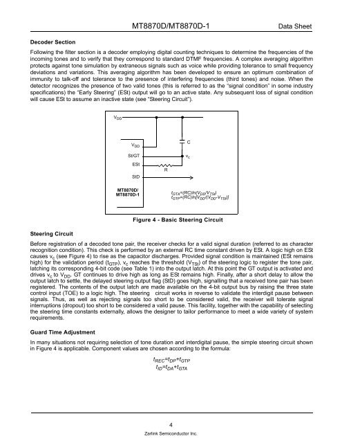
V DD<br />
V DD<br />
St/GT<br />
ESt<br />
StD<br />
MT8870D/<br />
MT8870D-1<br />
R<br />
Figure 4 - Basic Steering Circuit<br />
Steering Circuit<br />
Before registration of a decoded tone pair, the receiver checks for a valid signal duration (referred to as character<br />
recognition condition). This check is performed by an external RC time constant driven by ESt. A logic high on ESt<br />
causes vc (see Figure 4) to rise as the capacitor discharges. Provided signal condition is maintained (ESt remains<br />
high) for the validation period (tGTP), vc reaches the threshold (VTSt) of the steering logic to register the tone pair,<br />
latching its corresponding 4-bit code (see Table 1) into the output latch. At this point the GT output is activated and<br />
drives vc to VDD . GT continues to drive high as long as ESt remains high. Finally, after a short delay to allow the<br />
output latch to settle, the delayed steering output flag (StD) goes high, signalling that a received tone pair has been<br />
registered. The contents of the output latch are made available on the 4-bit output bus by raising the three state<br />
control input (TOE) to a logic high. The steering circuit works in reverse to validate the interdigit pause between<br />
signals. Thus, as well as rejecting signals too short to be considered valid, the receiver will tolerate signal<br />
interruptions (dropout) too short to be considered a valid pause. This facility, together with the capability of selecting<br />
the steering time constants externally, allows the designer to tailor performance to meet a wide variety of system<br />
requirements.<br />
Guard Time Adjustment<br />
In many situations not requiring selection of tone duration and interdigital pause, the simple steering circuit shown<br />
in Figure 4 is applicable. Component values are chosen according to the formula:<br />
t REC =t DP +t GTP<br />
t ID =t DA +t GTA<br />
4<br />
C<br />
v c<br />
t GTA=(RC)In(V DD/V TSt)<br />
t GTP =(RC)In[V DD /(V DD -V TSt )]<br />
<strong>Zarlink</strong> <strong>Semiconductor</strong> Inc.