MT8870DE1-1 - Zarlink Semiconductor
MT8870DE1-1 - Zarlink Semiconductor
MT8870DE1-1 - Zarlink Semiconductor

You also want an ePaper? Increase the reach of your titles
YUMPU automatically turns print PDFs into web optimized ePapers that Google loves.
MT8870D/MT8870D-1 Data Sheet<br />
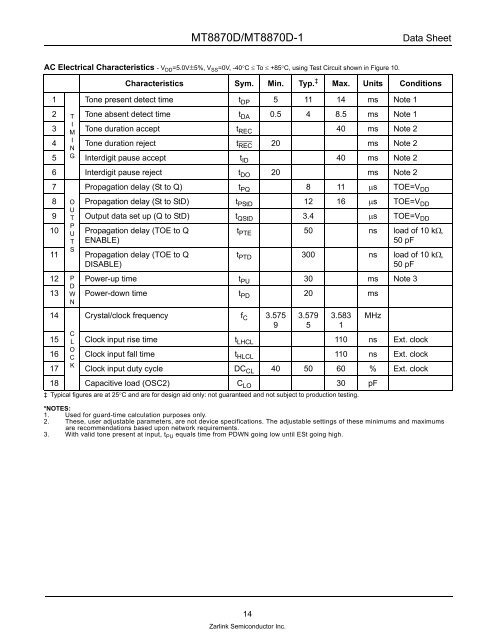
AC Electrical Characteristics - VDD =5.0V±5%, VSS =0V, -40°C ≤ To ≤ +85°C, using Test Circuit shown in Figure 10.<br />
Characteristics Sym. Min. Typ. ‡ Max. Units Conditions<br />
1 Tone present detect time tDP 5 11 14 ms Note 1<br />
2 T Tone absent detect time tDA 0.5 4 8.5 ms Note 1<br />
3<br />
I<br />
M Tone duration accept tREC 40 ms Note 2<br />
4<br />
I<br />
N<br />
Tone duration reject tREC 20 ms Note 2<br />
5 G Interdigit pause accept tID 40 ms Note 2<br />
6 Interdigit pause reject tDO 20 ms Note 2<br />
7 Propagation delay (St to Q) tPQ 8 11 µs TOE=VDD 8<br />
9<br />
O<br />
U<br />
T<br />
Propagation delay (St to StD)<br />
Output data set up (Q to StD)<br />
tPStD tQStD 12<br />
3.4<br />
16 µs<br />
µs<br />
TOE=VDD TOE=VDD 10<br />
P<br />
U<br />
T<br />
Propagation delay (TOE to Q<br />
ENABLE)<br />
tPTE 50 ns load of 10 kΩ,<br />
50 pF<br />
11<br />
S<br />
Propagation delay (TOE to Q<br />
DISABLE)<br />
tPTD 300 ns load of 10 kΩ,<br />
50 pF<br />
12<br />
13<br />
P<br />
D<br />
W<br />
N<br />
Power-up time<br />
Power-down time<br />
tPU tPD 30<br />
20<br />
ms<br />
ms<br />
Note 3<br />
14 Crystal/clock frequency fC 3.575<br />
9<br />
3.579<br />
5<br />
3.583<br />
1<br />
MHz<br />
15<br />
C<br />
L Clock input rise time tLHCL 110 ns Ext. clock<br />
16<br />
O<br />
C Clock input fall time tHLCL 110 ns Ext. clock<br />
17<br />
K<br />
Clock input duty cycle DCCL 40 50 60 % Ext. clock<br />
18 Capacitive load (OSC2) CLO 30 pF<br />
‡ Typical figures are at 25°C and are for design aid only: not guaranteed and not subject to production testing.<br />
*NOTES:<br />
1. Used for guard-time calculation purposes only.<br />
2. These, user adjustable parameters, are not device specifications. The adjustable settings of these minimums and maximums<br />
are recommendations based upon network requirements.<br />
3. With valid tone present at input, t PU equals time from PDWN going low until ESt going high.<br />
14<br />
<strong>Zarlink</strong> <strong>Semiconductor</strong> Inc.