TDA18218HN DVB-T Silicon Tuner IC - NXP.com
TDA18218HN DVB-T Silicon Tuner IC - NXP.com
TDA18218HN DVB-T Silicon Tuner IC - NXP.com

You also want an ePaper? Increase the reach of your titles
YUMPU automatically turns print PDFs into web optimized ePapers that Google loves.
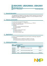
1. General description<br />
2. Features<br />
3. Applications<br />
<strong>TDA18218HN</strong><br />
<strong>DVB</strong>-T <strong>Silicon</strong> <strong>Tuner</strong> <strong>IC</strong><br />
Rev. 01 — 8 July 2009 Product data sheet<br />
The <strong>TDA18218HN</strong> is a <strong>Silicon</strong> <strong>Tuner</strong> <strong>IC</strong> designed for digital terrestrial (<strong>DVB</strong>-T) TV<br />
reception. The <strong>TDA18218HN</strong> integrates the overall tuning function, including selectivity<br />
and provides a low-IF output signal.<br />
The <strong>TDA18218HN</strong> uses integrated IF filters to support 6 MHz, 7 MHz or 8 MHz channel<br />
bandwidths. The <strong>TDA18218HN</strong> requires only one single 16 MHz crystal for clock<br />
generation. A clock signal is available on crystal oscillator output pins (XTO_P / XTO_N)<br />
to synchronize the channel decoder.<br />
The <strong>TDA18218HN</strong> is a low cost <strong>Silicon</strong> <strong>Tuner</strong> targeting digital terrestrial applications. The<br />
<strong>TDA18218HN</strong> matches the performance of the conventional can tuners. Additionally, the<br />
following benefits can be stated:<br />
• Easy on-board integration<br />
• Drastically reduces:<br />
– the size of the tuner function<br />
– the power consumption<br />
■ Fully integrated IF selectivity; eliminating the need for external SAW filters<br />
■ Fully integrated oscillators with no external <strong>com</strong>ponents<br />
■ Integrated wideband gain control<br />
■ Alignment free<br />
■ RF loop-through for easy implementation in the Set-Top Box (STB)<br />
■ Integrated die thermal sensor<br />
■ Single 3.3 V power supply<br />
■ Low power consumption (750 mW)<br />
■ Crystal oscillator output buffer (16 MHz) for single crystal applications<br />
■ I 2 C-bus interface <strong>com</strong>patible with 3.3 V and 5 V microcontrollers<br />
■ Three Standby modes<br />
■ RoHS packaging<br />
■ <strong>DVB</strong>-T Set-Top Box (STB) and TV receiver<br />
■ System application optimization is described in the application note AN0814<br />
■ Driver application is described in the application note AN0822
<strong>NXP</strong> Semiconductors <strong>TDA18218HN</strong><br />
4. Quick reference data<br />
Table 1. Quick reference data<br />
Tamb =25°C; VCC = 3.3 V; IF output level option = 2 V (p - p); IF output load =1kΩ on each terminal<br />
[1] Measured with TDA10048 channel decoder.<br />
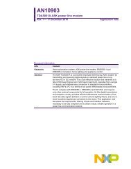
5. Ordering information<br />
6. Block diagram<br />
<strong>DVB</strong>-T <strong>Silicon</strong> <strong>Tuner</strong> <strong>IC</strong><br />
Symbol Parameter Conditions Min Typ Max Unit<br />
fRF RF frequency center of channel 174 - 864 MHz<br />
NFtun tuner noise figure normal mode; maximum gain - 5 7 dB<br />
ϕn phase noise worst case in the RF frequency range<br />
10 kHz - −85 - dBc/Hz<br />
100 kHz - −105 - dBc/Hz<br />
P power dissipation - 775 - mW<br />
Vi(max) maximum input voltage 1 dB gain <strong>com</strong>pression, one analog TV signal - 108 - dBμV<br />
αimage image rejection normal mode - 65 - dB<br />
Sdig digital sensitivity <strong>DVB</strong>-T (64 QAM 2/3); BER = 2 × 10⁻⁴ [1] - −82 - dBm<br />
RF_IN<br />
LT<br />
Fig 1. Block diagram<br />
1<br />
46<br />
Table 2. Ordering information<br />
Type number Package<br />
Name Description Version<br />
<strong>TDA18218HN</strong> HVQFN48 plastic thermal enhanced very thin quad flat package;<br />
no leads; 48 terminals; body 7 × 7 × 0.85 mm<br />
SOT619-1<br />
AGC1<br />
LEVEL<br />
CONTROL<br />
ATTENUATOR<br />
AGC2<br />
LEVEL<br />
CONTROL<br />
22 35<br />
AS SCL<br />
I 2 C<br />
INTERFACE<br />
BP<br />
FILTER<br />
36<br />
SDA<br />
SYNTHESIZER<br />
IF<br />
SELECTIVITY<br />
LPFc<br />
<strong>TDA18218HN</strong><br />
IFO_P<br />
IFO_N<br />
VIFAGC<br />
001aaj012<br />
<strong>TDA18218HN</strong>_1 © <strong>NXP</strong> B.V. 2009. All rights reserved.<br />
Product data sheet Rev. 01 — 8 July 2009 2 of 25<br />
14<br />
VTLO<br />
mixer<br />
15<br />
CPLO<br />
IF<br />
AGC<br />
CRYSTAL<br />
OSCILATOR<br />
16<br />
XTAL_P<br />
17<br />
XTAL_N<br />
31<br />
30<br />
32<br />
19<br />
20<br />
XTO_P<br />
XTO_N
<strong>NXP</strong> Semiconductors <strong>TDA18218HN</strong><br />
7. Pinning information<br />
7.1 Pinning<br />
Fig 2. Pin configuration<br />
7.2 Pin description<br />
terminal 1<br />
index area<br />
i.c.<br />
48<br />
47<br />
RF_IN 1 36 SDA<br />
i.c. 2 35 SCL<br />
i.c. 3 34 GND(DIG)<br />
GND(RF) 4 33 i.c.<br />
i.c. 5 32 VIFAGC<br />
i.c.<br />
GND(IF)<br />
6<br />
7<br />
<strong>TDA18218HN</strong><br />
31<br />
30<br />
IFO_P<br />
IFO_N<br />
VCC(IF) 8 29 VCC(IF)<br />
i.c. 9 28 GND(IF)<br />
CAPREG_VCO 10 27 REG28<br />
GND(VCO) 11 26 REG18<br />
VCC(PLL) 12 25 VT_K<br />
13<br />
14<br />
GND(PLL)<br />
VTLO<br />
VCC(RF)<br />
LT<br />
<strong>DVB</strong>-T <strong>Silicon</strong> <strong>Tuner</strong> <strong>IC</strong><br />
001aaj013<br />
<strong>TDA18218HN</strong>_1 © <strong>NXP</strong> B.V. 2009. All rights reserved.<br />
Product data sheet Rev. 01 — 8 July 2009 3 of 25<br />
46<br />
45<br />
15<br />
16<br />
CPLO<br />
VCC(RF)<br />
GND(RF)<br />
44<br />
43<br />
17<br />
18<br />
XTAL_P<br />
XTAL_N<br />
i.c.<br />
i.c.<br />
GND(RF)<br />
42<br />
41<br />
19<br />
20<br />
XTO_P<br />
XTO_N<br />
GND(RF)<br />
GND(RF)<br />
Transparent top view<br />
40<br />
39<br />
21<br />
22<br />
XTAL_MS<br />
AS<br />
i.c.<br />
GND(RF)<br />
CAPRFAGC<br />
38<br />
37<br />
23<br />
24<br />
GND(IF)<br />
CP_K<br />
Table 3. Pin description<br />
Symbol Pin Description<br />
RF_IN 1 unbalanced RF input<br />
i.c. 2 internally connected; leave open<br />
i.c. 3 internally connected; leave open<br />
GND(RF) 4 RF ground<br />
i.c. 5 internally connected; leave open<br />
i.c 6 internally connected; leave open<br />
GND(IF) 7 IF ground<br />
VCC(IF) 8 IF supply voltage (3.3 V)<br />
i.c. 9 internally connected; leave open<br />
CAPREG_VCO 10 VCO supply decoupling<br />
GND(VCO) 11 VCO ground<br />
VCC(PLL) 12 PLL supply voltage<br />
GND(PLL) 13 PLL ground<br />
VTLO 14 local oscillator (LO) tuning voltage input
<strong>NXP</strong> Semiconductors <strong>TDA18218HN</strong><br />
8. Functional description<br />
CPLO 15 charge pump of the LO synthesizer<br />
XTAL_P 16 crystal oscillator input positive<br />
XTAL_N 17 crystal oscillator input negative<br />
i.c. 18 internally connected; leave open<br />
XTO_P 19 crystal oscillator output buffer positive<br />
XTO_N 20 crystal oscillator output buffer negative<br />
XTAL_MS 21 XTAL out mode<br />
AS 22 I2C-bus address selection input<br />
GND(IF) 23 IF ground<br />
CP_K 24 charge pump of the calibration synthesizer<br />
VT_K 25 tuning voltage of the calibration synthesizer<br />
REG18 26 internal regulator decoupling<br />
REG28 27 internal regulator decoupling<br />
GND(IF) 28 IF ground<br />
VCC(IF) 29 IF supply voltage (3.3 V)<br />
IFO_N 30 IF output negative<br />
IFO_P 31 IF output positive<br />
VIFAGC 32 IF gain control input<br />
i.c. 33 internally connected; leave open<br />
GND(DIG) 34 digital ground<br />
SCL 35 I2C-bus clock input<br />
SDA 36 I2 Table 3. Pin description …continued<br />
Symbol Pin Description<br />
C-bus data input and output<br />
CAPRFAGC 37 RF AGC filtering<br />
GND(RF) 38 RF ground<br />
i.c. 39 internally connected; leave open<br />
GND(RF) 40 RF ground<br />
GND(RF) 41 RF ground<br />
GND(RF) 42 RF ground<br />
i.c. 43 internally connected; leave open<br />
GND(RF) 44 RF ground<br />
VCC(RF) 45 RF supply voltage<br />
LT 46 loop-through<br />
VCC(RF) 47 RF supply voltage<br />
i.c. 48 internally connected; leave open<br />
<strong>DVB</strong>-T <strong>Silicon</strong> <strong>Tuner</strong> <strong>IC</strong><br />
The RF input signal is driven to a low-noise amplifier. It is then amplified and fed to the<br />
image rejection mixer. The mixer down-converts the RF signal to a low IF frequency, which<br />
depends on channel bandwidth (standard IF filters are implemented for 6 MHz, 7 MHz<br />
<strong>TDA18218HN</strong>_1 © <strong>NXP</strong> B.V. 2009. All rights reserved.<br />
Product data sheet Rev. 01 — 8 July 2009 4 of 25
<strong>NXP</strong> Semiconductors <strong>TDA18218HN</strong><br />
<strong>DVB</strong>-T <strong>Silicon</strong> <strong>Tuner</strong> <strong>IC</strong><br />
and 8 MHz channel bandwidths). The <strong>TDA18218HN</strong> requires a single 16 MHz crystal for<br />
clock generation, a 16 MHz differential sine wave clock reference is available to drive a<br />
channel decoder.<br />
8.1 AGC1 stage<br />
The <strong>TDA18218HN</strong> embeds 2 different RF amplifiers with internal gain control.<br />
The first stage, AGC1, behaves like a LNA (Low noise amplifier); its gain can take 4<br />
different values (15 dB, 12 dB, 9 dB and 6 dB). Purpose of this amplifier is to ensure a low<br />
noise figure for the tuner.<br />
In order to optimize noise and linearity performances an internal level detector selects the<br />
appropriate gain:<br />
• If the signal level at the tuner is low, the gain is set to the maximum value (15 dB).<br />
• If the signal level at the tuner input is high, the gain is set to the minimum value (6 dB).<br />
• In between the gain is set to an intermediate value 12 dB or 9 dB.<br />
The strategy of the level detection is a proprietary algorithm from <strong>NXP</strong>, managed by the<br />
driver.<br />
It should be noted that:<br />
1. The level detector measures the signal level within the <strong>com</strong>plete RF frequency range,<br />
i.e. from 50 MHz to 870 MHz. Consequently, AGC1 gain is adapted to the <strong>com</strong>plete<br />
RF power. If a strong signal is present at the tuner input, it will determine AGC1 gain<br />
(even if it is not the wanted signal). This concept prevents the tuner from overloading.<br />
2. The level control is always operating.<br />
8.2 AGC2 stage<br />
The second stage, AGC2, is also an amplifier with a gain controlled thanks to a level<br />
detector.<br />
The gain is controlled between −12 dB and +16.4 dB, it is adapted by steps of 0.2 dB.<br />
It should be noted that:<br />
1. The level control is always operating. Consequently, this amplifier is responsible for<br />
adapting the daily level changes.<br />
2. The level detector measures the signal level within the <strong>com</strong>plete RF frequency range<br />
(same as AGC1)<br />
The strategy of the level detection is a proprietary algorithm from <strong>NXP</strong>, managed by the<br />
driver.<br />
8.3 IF AGC<br />
Finally, in order to adapt the tuner output level, a last amplifier is used (IF AGC). This<br />
amplifier delivers the appropriate level to the <strong>DVB</strong>-T channel decoder. The output level is<br />
therefore controlled thanks to the DC voltage applied on VIFAGC pin. This voltage is<br />
<strong>com</strong>monly delivered by the channel decoder.<br />
<strong>TDA18218HN</strong>_1 © <strong>NXP</strong> B.V. 2009. All rights reserved.<br />
Product data sheet Rev. 01 — 8 July 2009 5 of 25
<strong>NXP</strong> Semiconductors <strong>TDA18218HN</strong><br />
9. Control interface<br />
It should be noted that the level control is always operating.<br />
<strong>DVB</strong>-T <strong>Silicon</strong> <strong>Tuner</strong> <strong>IC</strong><br />
The strategy of the level detection has to be adapted for each type of channel decoder. It<br />
must be defined to satisfy ADC sampling (minimum level, ADC headroom).<br />
All AGC amplifiers are controlled independently.<br />
8.4 Power-down mode<br />
The <strong>TDA18218HN</strong> can be programmed in Standby mode. The following blocks are turned<br />
off when programming a power-down:<br />
• AGC2 and its level detector<br />
• BP filter<br />
• Mixer and VCO<br />
• IF selectivity LPFc<br />
• IF AGC<br />
Remaining functions are:<br />
• Loop-Through<br />
• 16 MHz clock output (to drive a channel decoder)<br />
• I 2 C-bus Core (to wake-up the <strong>IC</strong> later on)<br />
9.1 I2C-bus format, write and read mode<br />
I2C-bus uses two pins (SDA and SCL) to transfer information between devices connected<br />
to the bus. The SDA pin provides bidirectional data transfer. While the SCL pin provides<br />
the timing sequences. Data can be read and written as follows:<br />
Write mode:<br />
• Any register can be written to using its subaddress<br />
• Any following (contiguous) registers can be written using the subaddress of the first<br />
register<br />
Read mode:<br />
• The read after Restart mode is not allowed. In addition, registers cannot be read using<br />
the subaddress of the register. However, registers can be read as follows:<br />
– from 00h to 16h<br />
– from 00h to 27h<br />
– from 00h to 3Ah<br />
– from 00h to any register subaddress, if MSB = 1 for the next register<br />
<strong>TDA18218HN</strong>_1 © <strong>NXP</strong> B.V. 2009. All rights reserved.<br />
Product data sheet Rev. 01 — 8 July 2009 6 of 25
<strong>TDA18218HN</strong>_1 © <strong>NXP</strong> B.V. 2009. All rights reserved.<br />
Product data sheet Rev. 01 — 8 July 2009 7 of 25<br />
xxxxxxxxxxxxxxxxxxxxx xxxxxxxxxxxxxxxxxxxxxxxxxx xxxxxxx x x x xxxxxxxxxxxxxxxxxxxxxxxxxxxxxx xxxxxxxxxxxxxxxxxxx xx xx<br />
xxxxx xxxxxxxxxxxxxxxxxxxxxxxxxxx xxxxxxxxxxxxxxxxxxx xxxxxx xxxxxxxxxxxxxxxxxxxxxxxxxxxxxxxxxxx xxxxxxxxxxxx x x<br />
xxxxxxxxxxxxxxxxxxxxx xxxxxxxxxxxxxxxxxxxxxxxxxxxxxx xxxxx xxxxxxxxxxxxxxxxxxxxxxxxxxxxxxxxxxxxxxxxxxxxxxxxxx xxxxxxxx<br />
xxxxxxxxxxxxxxxxxxxxxxxxx xxxxxxxxxxxxxxxxxxxx xxx<br />
Table 4. I2C-bus register map<br />
Sub Register Bit Initial POR<br />
address<br />
7 (MSB) 6 5 4 3 2 1 0 (LSB)<br />
value<br />
(Hex)<br />
(Hex)<br />
Address byte 1 1 1 0 0 0 MA[1:0] R/W - -<br />
Address byte 2 0 0 AD[5:0] - -<br />
00h ID byte 1 ID[6:0] C0 [1] C0<br />
01h Read byte 1 - LO_Lock CAL_Lock - TM_D[3:0] 88 80<br />
02h Read byte 2 - 00 00<br />
03h Read byte 3 AGC2[7:0] 8E 3C<br />
04h Read byte 4 AGC1[2] - LT[1:0] AGC1[1:0] 03 00<br />
05h Read byte 5 - 00 00<br />
06h Read byte 6 - 00 00<br />
07h Main divider<br />
byte 1<br />
- D0 F0<br />
08h PSM byte 1 - 00 00<br />
09h Main divider<br />
byte 2<br />
- 40 40<br />
0Ah Main divider<br />
byte 3<br />
LO_Frac_0[31:24] 00 00<br />
0Bh Main divider<br />
byte 4<br />
LO_Frac_1[23:16] 00 00<br />
0Ch Main divider<br />
byte 5<br />
LO_Frac_2[15:12] - 07 00<br />
0Dh Main divider<br />
byte 6<br />
- FF 01<br />
0Eh Main divider<br />
byte 7<br />
- 84 84<br />
0Fh Main divider<br />
- Freq_prog_<br />
- 09 08<br />
byte 8<br />
Start<br />
10h Call divider<br />
byte 1<br />
- 00 00<br />
11h Call divider<br />
byte 2<br />
- 13 13<br />
12h Call divider<br />
byte 3<br />
- 00 00<br />
<strong>NXP</strong> Semiconductors <strong>TDA18218HN</strong><br />
<strong>DVB</strong>-T <strong>Silicon</strong> <strong>Tuner</strong> <strong>IC</strong>
<strong>TDA18218HN</strong>_1 © <strong>NXP</strong> B.V. 2009. All rights reserved.<br />
Product data sheet Rev. 01 — 8 July 2009 8 of 25<br />
xxxxxxxxxxxxxxxxxxxxx xxxxxxxxxxxxxxxxxxxxxxxxxx xxxxxxx x x x xxxxxxxxxxxxxxxxxxxxxxxxxxxxxx xxxxxxxxxxxxxxxxxxx xx xx<br />
xxxxx xxxxxxxxxxxxxxxxxxxxxxxxxxx xxxxxxxxxxxxxxxxxxx xxxxxx xxxxxxxxxxxxxxxxxxxxxxxxxxxxxxxxxxx xxxxxxxxxxxx x x<br />
xxxxxxxxxxxxxxxxxxxxx xxxxxxxxxxxxxxxxxxxxxxxxxxxxxx xxxxx xxxxxxxxxxxxxxxxxxxxxxxxxxxxxxxxxxxxxxxxxxxxxxxxxx xxxxxxxx<br />
xxxxxxxxxxxxxxxxxxxxxxxxx xxxxxxxxxxxxxxxxxxxx xxx<br />
Table 4. I 2 C-bus register map …continued<br />
Sub<br />
address<br />
Register Bit Initial<br />
7 (MSB) 6 5 4 3 2 1 0 (LSB)<br />
value<br />
(Hex)<br />
13h Call divider<br />
byte 4<br />
14h Call divider<br />
byte 5<br />
15h Call divider<br />
byte 6<br />
16h Call divider<br />
byte 7<br />
17h Power-down<br />
byte 1<br />
18h Power-down<br />
byte 2<br />
- pdLT - pdAGC1b PD_RFAGC<br />
_Ifout<br />
- RFSW_MTO<br />
_LT_RFin<br />
- 00 00<br />
- 01 01<br />
- 84 84<br />
- 09 09<br />
PD_LO_<br />
Synthe<br />
SM F0 [2]<br />
B0 [3]<br />
- pdDETECT1 pdAGC2b - 19 [2]<br />
19h XTOUT byte - XtOut[3:0] 0A 0A<br />
1Ah IF byte 1 - IF_level[2:0] - BP_Filter[2:0] 8E 86<br />
1Bh IF byte 2 - LP_Fc[1:0] 69 6A<br />
1Ch AGC2b byte pulse_up_<br />
pulse_up_<br />
AGC_On - 98 98<br />
auto<br />
width[1:0]<br />
1Dh PSM byte 2 TM_<br />
Range<br />
TM_ON - 01 C3<br />
1Eh PSM byte 3 - 00 00<br />
1Fh PSM byte 4 AGC1_Speed[1:0] - AGC1_<br />
aud_sel<br />
AGC1_au_ptr[1:0] 58 58<br />
20h AGC1 byte 1 AGC2_RAM_sel[1:0] AGC2_ AGC1_ Manual_LT AGC1_aud[2:0] 10 00<br />
Gup_sel Gup_sel<br />
21h AGC1 byte 2 AGC2_Speed[1:0] - AGC1_Gud[4:0] 40 40<br />
22h AGC1 byte 3 - 8C 80<br />
23h AGC2 byte 1 - AGC2_Gud[4:0] 00 00<br />
24h AGC2 byte 2 - 0C 0C<br />
25h Analog AGC<br />
byte<br />
- IFAGC_Top[3:0] 48 48<br />
26h RC byte - 85 80<br />
27h RSSI byte - C9 8E<br />
59 [3]<br />
POR<br />
(Hex)<br />
B5<br />
59<br />
<strong>NXP</strong> Semiconductors <strong>TDA18218HN</strong><br />
<strong>DVB</strong>-T <strong>Silicon</strong> <strong>Tuner</strong> <strong>IC</strong>
<strong>TDA18218HN</strong>_1 © <strong>NXP</strong> B.V. 2009. All rights reserved.<br />
Product data sheet Rev. 01 — 8 July 2009 9 of 25<br />
xxxxxxxxxxxxxxxxxxxxx xxxxxxxxxxxxxxxxxxxxxxxxxx xxxxxxx x x x xxxxxxxxxxxxxxxxxxxxxxxxxxxxxx xxxxxxxxxxxxxxxxxxx xx xx<br />
xxxxx xxxxxxxxxxxxxxxxxxxxxxxxxxx xxxxxxxxxxxxxxxxxxx xxxxxx xxxxxxxxxxxxxxxxxxxxxxxxxxxxxxxxxxx xxxxxxxxxxxx x x<br />
xxxxxxxxxxxxxxxxxxxxx xxxxxxxxxxxxxxxxxxxxxxxxxxxxxx xxxxx xxxxxxxxxxxxxxxxxxxxxxxxxxxxxxxxxxxxxxxxxxxxxxxxxx xxxxxxxx<br />
xxxxxxxxxxxxxxxxxxxxxxxxx xxxxxxxxxxxxxxxxxxxx xxx<br />
Table 4. I 2 C-bus register map …continued<br />
Sub Register Bit Initial POR<br />
address<br />
7 (MSB) 6 5 4 3 2 1 0 (LSB)<br />
value<br />
(Hex)<br />
(Hex)<br />
28h IR CAL byte 1 - A7 F5<br />
29h IR CAL byte 2 - 00 30<br />
2Ah IR CAL byte 3 - 00 30<br />
2Bh IR CAL byte 4 - 00 00<br />
2Ch RF CAL byte 1 - 30 30<br />
2Dh RF CAL byte 2 - 81 80<br />
2Eh RF CAL byte 3 - 80 00<br />
2Fh RF CAL byte 4 - 00 00<br />
30h RF CAL byte 5 - 39 36<br />
31h RF CAL byte 6 - 00 00<br />
32h RF CAL byte 7 - 8A 8A<br />
33h RF CAL byte 8 - 00 00<br />
34h RF CAL byte 9 - 00 00<br />
35h RF CAL byte 10 - 00 00<br />
36h RF CAL RAM<br />
byte 1<br />
- 00 00<br />
37h RF CAL RAM<br />
byte 2<br />
- 00 00<br />
38h Margin byte - 00 00<br />
39h Fmax byte 1 - F6 F6<br />
3Ah Fmax byte 2 - F6 F6<br />
[1] See Section 9.2.1 “Device type address ID”.<br />
[2] Case <strong>TDA18218HN</strong> is a device without LT.<br />
[3] Case <strong>TDA18218HN</strong> is a device with LT.<br />
<strong>NXP</strong> Semiconductors <strong>TDA18218HN</strong><br />
<strong>DVB</strong>-T <strong>Silicon</strong> <strong>Tuner</strong> <strong>IC</strong>
<strong>NXP</strong> Semiconductors <strong>TDA18218HN</strong><br />
9.2 I 2 C-bus address selection<br />
<strong>DVB</strong>-T <strong>Silicon</strong> <strong>Tuner</strong> <strong>IC</strong><br />
The programmable module address bits MA[1:0] allow up to four tuners to be addressed<br />
in one system. Bits MA[1:0] are programmed by applying a specific voltage (VAS) to pin<br />
AS. The relationship between the status of bits MA[1:0] and the voltage applied to pin AS<br />
is shown in Table 5.<br />
Table 5. Address byte 1 bit descriptions<br />
Legend: * power-on reset value.<br />
Bit Symbol Access Value Description<br />
7 to 3 - R/W 1 1000* must be set to 1 1000<br />
2 to 1 MA[1:0] R/W programmable address bit value set with VAS<br />
00 VAS = 0 V to 0.1 × VCC<br />
Example: MA[1:0] = 00, R/W = 0, full module address = 1100 0000 (C0h).<br />
9.2.1 Device type address ID<br />
9.3 Crystal buffer output<br />
01 VAS = 0.2 × VCC to 0.3 × VCC<br />
10 VAS = 0.4 × VCC to 0.6 × VCC<br />
11 VAS = 0.9 × VCC to VCC<br />
0 R/W R/W 0 write mode<br />
1 read mode<br />
Table 6. Address byte 2 bit descriptions<br />
Legend: * power-on reset value.<br />
Bit Symbol Access Value Description<br />
7 to 6 - R/W 00* must be set to 00<br />
5 to 0 AD[5:0] R/W - programmable address bits of the first<br />
programming byte<br />
Table 7. ID byte bit descriptions<br />
Legend: * power-on reset value.<br />
Address Register Bit Symbol Access Value Description<br />
00h ID byte 7 - R 1* must be 1<br />
6 to 0 ID[6:0] R 100 0000* <strong>TDA18218HN</strong> device type address<br />
<strong>TDA18218HN</strong> embeds a Xtal oscillator and a buffer to drive another <strong>IC</strong>. The buffer can be<br />
configured through register XTOUT (I 2 C-bus sub address 19h). This buffer has been<br />
designed to be AC coupled. This output can be used in differential or sinusoidal mode<br />
(using XTO_N and XTO_P pins) or in asymmetrical or square mode (just leaving one pin<br />
open).<br />
It should be noted that <strong>TDA18218HN</strong> specification refers to differential output with no<br />
load.<br />
<strong>TDA18218HN</strong>_1 © <strong>NXP</strong> B.V. 2009. All rights reserved.<br />
Product data sheet Rev. 01 — 8 July 2009 10 of 25
<strong>NXP</strong> Semiconductors <strong>TDA18218HN</strong><br />
Table 8. Crystal buffer output register bit descriptions<br />
9.4 Temperature sensor<br />
[1] The die temperature can be read as shown in Table 10.<br />
<strong>DVB</strong>-T <strong>Silicon</strong> <strong>Tuner</strong> <strong>IC</strong><br />
Address Register Bit Symbol Access Value Description<br />
19h XTOUT byte 3 to 0 XtOut[3:0] R/W crystal buffer output<br />
0 XTAL off<br />
1 XTOUT off<br />
2 square wave 16 MHz<br />
7 sine wave 200 mV<br />
8 sine wave 400 mV<br />
9 sine wave 800 mV<br />
10 sine wave 1200 mV<br />
other not applicable<br />
Table 9. Temperature sensor bit descriptions<br />
Address Register Bit Symbol Access Value Description<br />
1Dh PSM byte 2 6 TM_ON W temperature sensor on or off<br />
0 temperature sensor switched off<br />
1 temperature sensor switched on<br />
7 TM_Range R/W temperature range selection<br />
0 60 °C to 90 °C<br />
1 92 °C to 122 °C<br />
01h Read byte 1 3 to 0 TM_D[3:0] R - die temperature [1]<br />
Table 10. Die temperature values<br />
TM_D[3:0] Temperature range selection (die temperature)<br />
TM_RANGE = 0 TM_RANGE = 1<br />
0000 60 °C 92 °C<br />
0001 62 °C 94 °C<br />
0010 66 °C 98 °C<br />
0011 64 °C 96 °C<br />
0100 74 °C 106 °C<br />
0101 72 °C 104 °C<br />
0110 68 °C 100 °C<br />
0111 70 °C 102 °C<br />
1000 90 °C 122 °C<br />
1001 88 °C 120 °C<br />
1010 84 °C 116 °C<br />
1011 86 °C 118 °C<br />
1100 76 °C 108 °C<br />
<strong>TDA18218HN</strong>_1 © <strong>NXP</strong> B.V. 2009. All rights reserved.<br />
Product data sheet Rev. 01 — 8 July 2009 11 of 25
<strong>NXP</strong> Semiconductors <strong>TDA18218HN</strong><br />
Table 10. Die temperature values …continued<br />
TM_D[3:0] Temperature range selection (die temperature)<br />
1101 78 °C 110 °C<br />
1110 82 °C 114 °C<br />
1111 80 °C 112 °C<br />
9.5 Standby mode selection<br />
Table 11. Standby mode selection<br />
9.6 IF level<br />
<strong>DVB</strong>-T <strong>Silicon</strong> <strong>Tuner</strong> <strong>IC</strong><br />
Refer to Table 21 “General characteristics for TV reception (RF input to IF output)”.<br />
9.7 AGC and band-pass filters<br />
TM_RANGE = 0 TM_RANGE = 1<br />
Mode Power down byte 1 (address 17h)<br />
SM (bit 0) pdAGC1b (bit 3) XTOUT<br />
Device-off mode 1 1 see Table 8<br />
Standby mode with loop-through and crystal<br />
oscillator on (default at POR), XTOUT 1200 mV<br />
1 0 see Table 8<br />
Standby mode with only crystal oscillator on 1 1 see Table 8<br />
Table 12. AGC and band-pass filter bit descriptions<br />
Address Register Bit Symbol Access Value Description<br />
03h Read byte 3 7 to 0 AGC2[7:0] R/W - AGC2 gain = 0.2 × (AGC2[7:0]) − 12 (dB)<br />
range = −12 dB to 16.4 dB<br />
04h Read byte 4 7 and AGC1[2:0] R/W AGC1 gain range = 6 dB to 15 dB<br />
1 to 0<br />
0 6 dB<br />
1 9 dB<br />
2 12 dB<br />
3 15 dB<br />
1Ah IF byte 1 2 to 0 BP_Filter[2:0] W band-pass filters<br />
3 filter 3 (174 MHz to 188 MHz)<br />
4 filter 4 (188 MHz to 253 MHz)<br />
5 filter 5 (253 MHz to 343 MHz)<br />
6 filter 6 (343 MHz to 870 MHz; bypass)<br />
1Bh IF byte 2 1 to 0 LP_Fc[1:0] W low-pass filter cut-off frequency<br />
0 6 MHz<br />
1 7 MHz<br />
2 8 MHz<br />
1Ch AGC2b byte 4 AGC_On W AGC1 and AGC2 clock on or off<br />
0 off<br />
1 on<br />
<strong>TDA18218HN</strong>_1 © <strong>NXP</strong> B.V. 2009. All rights reserved.<br />
Product data sheet Rev. 01 — 8 July 2009 12 of 25
<strong>NXP</strong> Semiconductors <strong>TDA18218HN</strong><br />
9.8 RFin to LT path<br />
Table 13. RFin to LT path bit descriptions<br />
9.9 PLL settings<br />
<strong>DVB</strong>-T <strong>Silicon</strong> <strong>Tuner</strong> <strong>IC</strong><br />
Address Register Bit Symbol Access Value Description<br />
20h AGC1 byte 1 3 Manual_LT W loop-through <strong>com</strong>mand<br />
0 sets LT attenuation depending on state of pin<br />
XTAL_MS; see Table 14<br />
1 sets LT attenuation manually; see Table 15<br />
04h Read byte 4 3 to 2 LT[1:0] R/W - sets LT gain in range: −6 dB to −15 dB; see Table 15<br />
Table 16. PLL bit descriptions<br />
Table 14. RFin to LT gain control modes<br />
Bit Manual_LT Pin XTAL_MS AGC1 and LT attenuator gain modes<br />
0 LOW AGC1 gain fixed at 6 dB; LT gain set by LT[1:0]; see Table 15<br />
0 HIGH LT gain set automatically function of AGC1 gain; see Table 15<br />
1 LOW AGC1 gain fixed at gain set by AGC1[2:0]; LT gain set by LT[1:0];<br />
see Table 15<br />
1 HIGH AGC1 gain set automatically; LT gain set by LT[1:0]; see<br />
Table 15<br />
Table 15. Loop-through attenuator gain settings<br />
LT[1] LT[0] Loop-through gain<br />
0 0 −6 dB<br />
0 1 −9 dB<br />
1 0 −12 dB<br />
1 1 −15 dB<br />
Address Register Bit Symbol Access Value Description<br />
0Ah Main divider byte 3 7 to 0 LO_Frac_0[31:24] R - LO frequency setting (kHz); in automatic mode<br />
0Bh Main divider byte 4 7 to 0 LO_Frac_1[23:16]<br />
0Ch Main divider byte 5 7 to 4 LO_Frac_2[15:12]<br />
01h Read byte 1 6 LO_Lock R LO lock flag<br />
0 PLL unlocked<br />
1 PLL locked<br />
5 CAL_Lock R calibration oscillator lock flag<br />
0 PLL unlocked<br />
1 PLL locked<br />
0Fh Main divider byte 8 6 Freq_prog_Start W 1 launch automatic mode of PLL calculation (LO<br />
and calibration synthesizer); automatically<br />
reset to logic 0 (internally) when LO and<br />
calibration are <strong>com</strong>pleted<br />
<strong>TDA18218HN</strong>_1 © <strong>NXP</strong> B.V. 2009. All rights reserved.<br />
Product data sheet Rev. 01 — 8 July 2009 13 of 25
<strong>NXP</strong> Semiconductors <strong>TDA18218HN</strong><br />
9.10 Power-down and switches<br />
[1] This setting controls the status of the Low Noise Amplifier (LNA).<br />
[2] RFSW_MTO_LT_RFin = 0 in tuner applications with loop-through disabled.<br />
RFSW_MTO_LT_RFin = 1 in tuner applications with loop-through enabled.<br />
10. Limiting values<br />
<strong>DVB</strong>-T <strong>Silicon</strong> <strong>Tuner</strong> <strong>IC</strong><br />
Table 17. Power-down and switches bit descriptions<br />
Address Register Bit Symbol Acces<br />
s<br />
Value Description<br />
17h Power-down byte 1 6 pdLT R/W loop-through output switch<br />
0 closed<br />
1 open<br />
3 pdAGC1b AGC1 power-down [1]<br />
0 LNA on<br />
1 LNA off<br />
2 PD_RFAGC_Ifout mixer and IF stages power-down<br />
0 blocks on<br />
1 blocks off<br />
1 PD_LO_Synthe LO synthesizer power-down<br />
0 PLL on<br />
1 PLL off<br />
0 SM Standby mode; I2C-bus interface, crystal<br />
oscillator and AGC1 are turned on<br />
0 normal<br />
1 standby<br />
18h Power-down byte 2 6 RFSW_MTO_LT_RFin R/W provides the RF signal to the<br />
loop-through [2]<br />
0 switch is open<br />
1 switch is closed<br />
2 pdDETECT1 AGC1 detector power-down<br />
0 detector on<br />
1 detector off<br />
1 pdAGC2b AGC2 power-down [1]<br />
0 LNA on<br />
1 LNA off<br />
Table 18. Limiting values<br />
In accordance with the Absolute Maximum Rating System (IEC 60134).<br />
Symbol Parameter Conditions Min Max Unit<br />
VCC supply voltage −0.3 +3.60 V<br />
<strong>TDA18218HN</strong>_1 © <strong>NXP</strong> B.V. 2009. All rights reserved.<br />
Product data sheet Rev. 01 — 8 July 2009 14 of 25
<strong>NXP</strong> Semiconductors <strong>TDA18218HN</strong><br />
[1] Class III: 200 V to 1000 V.<br />
11. Thermal characteristics<br />
12. Characteristics<br />
Table 18. Limiting values …continued<br />
In accordance with the Absolute Maximum Rating System (IEC 60134).<br />
[1] Channel loading assumptions: 129 channels at 75 dBμV.<br />
<strong>DVB</strong>-T <strong>Silicon</strong> <strong>Tuner</strong> <strong>IC</strong><br />
Symbol Parameter Conditions Min Max Unit<br />
VI input voltage pins SDA and SCL<br />
all other pins<br />
−0.3 +5.5 V<br />
VCC < 3.3 V −0.3 VCC + 0.3 V<br />
VCC > 3.3 V −0.3 +3.6 V<br />
Tstg storage temperature −40 +150 °C<br />
Tj junction temperature - +95 °C<br />
VESD electrostatic discharge voltage EIA/JESD22-A114<br />
(human body model)<br />
±2000 - V<br />
EIA/JESD22-C101-C<br />
(FCDM) class III [1]<br />
±200 - V<br />
Table 19. Thermal characteristics<br />
Symbol Parameter Conditions Min Typ Max Unit<br />
Rth(j-a)<br />
thermal resistance from<br />
junction to ambient<br />
according to JEDEC specification<br />
4L board with 16<br />
thermal vias<br />
- 29.9 - K/W<br />
Tamb ambient temperature - 0 - +70 °C<br />
Table 20. Loop-through characteristics (RF input to loop-through output)<br />
Tamb =25°C, VCC = 3.3 V; unless otherwise specified.<br />
Symbol Parameter Conditions Min Typ Max Unit<br />
fRF(lt) loop-through RF frequency center of channel 54 - 864 MHz<br />
|s11| 2 input return loss 75 Ω nominal impedance - −8 - dB<br />
|s22| 2 output return loss 75 Ω nominal impedance - −8 - dB<br />
Gv(lt) loop-through voltage gain 75 Ω load - −0.5 - dB<br />
ΔGlt loop-through gain variation in the RF frequency range; 75 Ω load - 2 4 dB<br />
NFlt loop-through noise figure maximum gain - 6 - dB<br />
CSOlt loop-through <strong>com</strong>posite second-order<br />
distortion<br />
[1] - −51 - dBc<br />
CTBlt loop-through <strong>com</strong>posite triple beat [1] - −55 - dBc<br />
αisol(bp) bypass isolation from loop-through output to RF input - 40 - dB<br />
<strong>TDA18218HN</strong>_1 © <strong>NXP</strong> B.V. 2009. All rights reserved.<br />
Product data sheet Rev. 01 — 8 July 2009 15 of 25
<strong>NXP</strong> Semiconductors <strong>TDA18218HN</strong><br />
<strong>DVB</strong>-T <strong>Silicon</strong> <strong>Tuner</strong> <strong>IC</strong><br />
Table 21. General characteristics for TV reception (RF input to IF output)<br />
Tamb =25°C, VCC = 3.3 V, IF output level option 2 V (p - p), IF output load = 1 kΩ on each pin; unless otherwise specified.<br />
Symbol Parameter Conditions Min Typ Max Unit<br />
VCC supply voltage 3.13 3.30 3.47 V<br />
<strong>IC</strong>C supply current normal mode [1] - 235 [2] 270 [3] mA<br />
device-off mode - 3 - mA<br />
Standby mode with loop-through<br />
and crystal oscillator on (default at<br />
POR), XTOUT 1200 mV<br />
- 60 - mA<br />
Standby mode with only oscillator on - 22 - mA<br />
P power dissipation - 775 - mW<br />
fRF RF frequency center of channel 174 - 864 MHz<br />
fIF(nom) nominal IF frequency center of channel; for channel bandwidth<br />
6 MHz - 3 - MHz<br />
7 MHz - 3.5 - MHz<br />
8 MHz - 4 - MHz<br />
Gv voltage gain normal mode 70 76 - dB<br />
ΔGAGC(tun) tuner AGC gain range normal mode - 63 - dB<br />
NFtun tuner noise figure normal mode; maximum gain - 5 7 dB<br />
Vo(IF)dif(p-p) peak-to-peak differential IF output IF_level[2:0] = 000 - 2 - V<br />
voltage<br />
IF_level[2:0] = 010 - 1 - V<br />
IF_level[2:0] = 111 - 0.5 - V<br />
Zo(IF) IF output impedance differential mode; magnitude value - 100 - Ω<br />
ΔGAGC(IF) IF AGC GAIN range 2 V (peak-to-peak) IF output voltage<br />
selection<br />
- 30 - dB<br />
Gtlt tilt gain RF frequency range [4]<br />
6 MHz IF filter (1 MHz to 5.5 MHz) - - 4 dB<br />
7 MHz IF filter (1 MHz to 6.5 MHz) - - 4 dB<br />
8 MHz IF filter (1 MHz to 7.5 MHz) - - 4 dB<br />
fIF(stpb)lp low-pass stop-band IF frequency 60 dB attenuation<br />
6 MHz IF filter (1 MHz to 5.5 MHz) - 12 - MHz<br />
7 MHz IF filter (1 MHz to 6.5 MHz) - 14 - MHz<br />
8 MHz IF filter (1 MHz to 7.5 MHz) - 16 - MHz<br />
αimage image rejection normal mode - 65 - dB<br />
td(grp) group delay time normal mode<br />
6 MHz IF filter (1 MHz to 5.5 MHz) - 155 - ns<br />
7 MHz IF filter (1 MHz to 6.5 MHz) - 165 - ns<br />
8 MHz IF filter (1 MHz to 7.5 MHz) - 175 - ns<br />
ϕn phase noise worst case in the RF frequency<br />
range<br />
10 kHz - −85 - dBc/Hz<br />
100 kHz - −105 - dBc/Hz<br />
tstartup(tun) tuner start-up time at power-up - - 1 s<br />
<strong>TDA18218HN</strong>_1 © <strong>NXP</strong> B.V. 2009. All rights reserved.<br />
Product data sheet Rev. 01 — 8 July 2009 16 of 25
<strong>NXP</strong> Semiconductors <strong>TDA18218HN</strong><br />
[1] XTAL buffer off.<br />
[2] Measured at 3.3 V.<br />
[3] Measured at 3.47 V.<br />
[4] Difference defined between maximum and minimum over the IF bandwidth.<br />
[5] Measured with TDA10048 channel decoder.<br />
<strong>DVB</strong>-T <strong>Silicon</strong> <strong>Tuner</strong> <strong>IC</strong><br />
Table 21. General characteristics for TV reception (RF input to IF output) …continued<br />
Tamb =25°C, VCC = 3.3 V, IF output level option 2 V (p - p), IF output load = 1 kΩ on each pin; unless otherwise specified.<br />
Symbol Parameter Conditions Min Typ Max Unit<br />
tset setting time channel change - - 60 ms<br />
ftun(step) tuner frequency (step size) - 1 - kHz<br />
Vi(max) maximum input voltage 1 dB gain <strong>com</strong>pression, one analog<br />
TV signal<br />
- 108 - dBμV<br />
Sdig digital sensitivity <strong>DVB</strong>-T (64 QAM 2/3);<br />
BER = 2 × 10 −4<br />
Table 22. Pin characteristics<br />
Tamb =25°C, VCC = 3.3 V; unless otherwise specified<br />
[5] - −82 - dBm<br />
Symbol Parameter Conditions Min Typ Max Unit<br />
IF AGC input: pin VIFAGC<br />
VAGC AGC voltage 0 - VCC V<br />
Zi input impedance [1] - - - MΩ<br />
dGAGC/dV rate of change of AGC gain<br />
with voltage<br />
- 30 55 dB/V<br />
Crystal oscillator<br />
fxtal crystal frequency - 16 - MHz<br />
Zi input impedance magnitude value; crystal<br />
specification: Rs = 150 Ω max;<br />
drive level < 100 μW<br />
- 500 - Ω<br />
Crystal oscillator output buffer<br />
Square mode: only on XTO_N (XtOut[3:0] = 2)<br />
Ro output resistance 16 MHz output frequency - 90 - Ω<br />
Vo(p-p) peak-to-peak output voltage 10 kΩ; 10 pF AC load; same load<br />
on XTO_P and XTO_N<br />
- 0.6 - V<br />
SRr slew rate of rising signal 10 kΩ; 10 pF AC load - 150 - V/μs<br />
SRf slew rate of falling signal 10 kΩ; 10 pF AC load - 80 - V/μs<br />
Sinusoidal mode: on XTO_P and XTO_N (XtOut[3:0] = 8)<br />
Ro output resistance 16 MHz output frequency - 480 - Ω<br />
Vo(p-p) peak-to-peak output voltage 10 kΩ; 10 pF AC load; same load<br />
on XTO_P and XTO_N<br />
- 0.4 - V<br />
Digital levels I2C-bus [2]<br />
Pin SCL<br />
VIL LOW-level input voltage fixed input levels - - 1.5 V<br />
VDD related input levels - - 0.3 × VCC V<br />
VIH HIGH-level input voltage fixed input levels 3 - - V<br />
VDD related input levels 0.7 × VCC - - V<br />
<strong>TDA18218HN</strong>_1 © <strong>NXP</strong> B.V. 2009. All rights reserved.<br />
Product data sheet Rev. 01 — 8 July 2009 17 of 25
<strong>NXP</strong> Semiconductors <strong>TDA18218HN</strong><br />
<strong>DVB</strong>-T <strong>Silicon</strong> <strong>Tuner</strong> <strong>IC</strong><br />
Table 22. Pin characteristics …continued<br />
Tamb =25°C, VCC = 3.3 V; unless otherwise specified<br />
Symbol Parameter Conditions Min Typ Max Unit<br />
fSCL<br />
pin SDA<br />
SCL clock frequency - - 400 kHz<br />
VOH HIGH-level output voltage ISDA = 3 mA (sink current) - - 0.4 V<br />
VIL LOW-level input voltage fixed input levels - - 1.5 V<br />
VDD related input levels - - 0.3 × VCC V<br />
VIH HIGH-level input voltage fixed input levels 3 - - V<br />
VDD related input levels 0.7 × VCC - - V<br />
[1] Typical value is HIGH impedance input.<br />
[2] Devices that use non-standard supply voltages, which do not conform to the intended I2C-bus system levels, must relate their input<br />
levels to the supply voltage to which the pull-up resistors are connected.<br />
<strong>TDA18218HN</strong>_1 © <strong>NXP</strong> B.V. 2009. All rights reserved.<br />
Product data sheet Rev. 01 — 8 July 2009 18 of 25
<strong>TDA18218HN</strong>_1 © <strong>NXP</strong> B.V. 2009. All rights reserved.<br />
Product data sheet Rev. 01 — 8 July 2009 19 of 25<br />
xxxxxxxxxxxxxxxxxxxxx xxxxxxxxxxxxxxxxxxxxxxxxxx xxxxxxx x x x xxxxxxxxxxxxxxxxxxxxxxxxxxxxxx xxxxxxxxxxxxxxxxxxx xx xx<br />
xxxxx xxxxxxxxxxxxxxxxxxxxxxxxxxx xxxxxxxxxxxxxxxxxxx xxxxxx xxxxxxxxxxxxxxxxxxxxxxxxxxxxxxxxxxx xxxxxxxxxxxx x x<br />
xxxxxxxxxxxxxxxxxxxxx xxxxxxxxxxxxxxxxxxxxxxxxxxxxxx xxxxx xxxxxxxxxxxxxxxxxxxxxxxxxxxxxxxxxxxxxxxxxxxxxxxxxx xxxxxxxx<br />
xxxxxxxxxxxxxxxxxxxxxxxxx xxxxxxxxxxxxxxxxxxxx xxx<br />
13. Application information<br />
3<br />
4<br />
5<br />
6<br />
7<br />
8<br />
9<br />
10<br />
11<br />
K1<br />
(1) Cxtal not connected for NDK; Cxtal = 1.5 pF for Siward.<br />
Fig 3. Application diagram<br />
1<br />
2<br />
RF_IN_OUT<br />
1 nF<br />
BAV99W<br />
1 nF<br />
BAV99W<br />
+3V3_TUN<br />
47 nF<br />
150 pF<br />
RF_IN<br />
1<br />
1 μH<br />
BLM18HK102SNI<br />
i.c.<br />
i.c.<br />
2<br />
3<br />
GND(RF)<br />
4<br />
i.c.<br />
5<br />
i.c.<br />
6<br />
470 pF<br />
GND(IF)<br />
VCC(IF)<br />
7<br />
8<br />
i.c.<br />
9<br />
CAPREG_VCO<br />
10<br />
100 nF<br />
GND(VCO)<br />
VCC(PLL)<br />
11<br />
12<br />
+3V3_TUN<br />
150 pF<br />
1 μH<br />
BLM18HK102SNI<br />
470 pF<br />
47 nF<br />
390 Ω<br />
6.8 nF<br />
1 nF<br />
+3V3_TUN<br />
47 nF<br />
U14<br />
470 pF<br />
220 nF<br />
390 Ω<br />
+3V3_TUN<br />
47 nF<br />
<strong>TDA18218HN</strong><br />
GND<br />
13 14 15 16 17 18 19 20 21 22 23 24<br />
GND(PLL) 48<br />
CPLO<br />
VTLO 47<br />
46<br />
XTAL_P 45<br />
470 pF<br />
i.c.<br />
VCC(RF)<br />
LT<br />
VCC(RF)<br />
GND(RF)<br />
i.c.<br />
GND(RF)<br />
GND(RF)<br />
GND(RF)<br />
i.c.<br />
GND(RF)<br />
CAPRFAGC<br />
XTAL_N 44<br />
i.c. 43<br />
XTO_P 42<br />
0.75 pF<br />
XTO_N 41<br />
Cxtal (1)<br />
XTAL_MS 40<br />
AS 39<br />
4.7 nF<br />
18 pF<br />
18 pF<br />
CP_K<br />
GND(IF) 38<br />
37<br />
QZ3<br />
220 nF<br />
36<br />
35<br />
34<br />
33<br />
32<br />
31<br />
30<br />
29<br />
28<br />
27<br />
26<br />
25<br />
SDA<br />
SCL<br />
GND(DIG)<br />
i.c.<br />
VIFAGC<br />
IFO_P<br />
IFO_N<br />
VCC(IF)<br />
GND(IF)<br />
REG28<br />
REG18<br />
VT_K<br />
16 MHz<br />
100 nF<br />
220 nF<br />
390 Ω<br />
XTOUT<br />
10 nF<br />
3.9 nF<br />
120 Ω<br />
6.8 nF<br />
100 nF<br />
100 nF<br />
100 nF<br />
+3V3_TUN<br />
4.7 kΩ<br />
4.7 kΩ<br />
470 pF 47 nF<br />
V_IF_AGC<br />
IF OUT P<br />
IF OUT N<br />
+3V3_TUN<br />
001aaj014<br />
<strong>NXP</strong> Semiconductors <strong>TDA18218HN</strong><br />
<strong>DVB</strong>-T <strong>Silicon</strong> <strong>Tuner</strong> <strong>IC</strong>
<strong>NXP</strong> Semiconductors <strong>TDA18218HN</strong><br />
14. Package outline<br />
HVQFN48: plastic thermal enhanced very thin quad flat package; no leads;<br />
48 terminals; body 7 x 7 x 0.85 mm<br />
DIMENSIONS (mm are the original dimensions)<br />
UNIT<br />
A<br />
A1 b c<br />
Dh Eh e e1 e2 L v w y y1 mm 1<br />
0.05<br />
0.00<br />
0.30<br />
0.18<br />
0.2<br />
7.1<br />
6.9<br />
5.25<br />
4.95<br />
7.1<br />
6.9<br />
5.25<br />
4.95<br />
0.5 5.5 5.5<br />
0.5<br />
0.3<br />
0.1 0.05 0.05 0.1<br />
(1)<br />
max.<br />
E (1)<br />
D (1)<br />
OUTLINE<br />
VERSION<br />
terminal 1<br />
index area<br />
L<br />
E h<br />
12<br />
1<br />
terminal 1<br />
index area<br />
48 37<br />
Dh Fig 4. Package outline HVQFN48 - SOT619-1<br />
0 2.5 5 mm<br />
REFERENCES<br />
scale<br />
IEC JEDEC JEITA<br />
SOT619-1 - - -<br />
MO-220 - - -<br />
D<br />
e 1<br />
25<br />
36<br />
EUROPEAN<br />
PROJECTION<br />
<strong>DVB</strong>-T <strong>Silicon</strong> <strong>Tuner</strong> <strong>IC</strong><br />
ISSUE DATE<br />
SOT619-1<br />
<strong>TDA18218HN</strong>_1 © <strong>NXP</strong> B.V. 2009. All rights reserved.<br />
Product data sheet Rev. 01 — 8 July 2009 20 of 25<br />
B A<br />
e<br />
1/2 e b<br />
v M C A B<br />
13 24 w M C<br />
Note<br />
1. Plastic or metal protrusions of 0.075 mm maximum per side are not included.<br />
e<br />
1/2 e<br />
E<br />
e 2<br />
A A1<br />
y 1 C<br />
detail X<br />
X<br />
C<br />
y<br />
c<br />
01-08-08<br />
02-10-18
<strong>NXP</strong> Semiconductors <strong>TDA18218HN</strong><br />
15. Abbreviations<br />
Table 23. Abbreviations<br />
Acronym Description<br />
ADC Analog-to-Digital Converter<br />
AGC Automatic Gain Control<br />
BER Bit Error Rate<br />
BP Band-Pass<br />
Cxtal crystal Capacitor<br />
<strong>DVB</strong>-T Digital Video Broadcasting – Terrestrial<br />
DVR Digital Video Recorder<br />
FCDM Flow Control Decision Message<br />
<strong>IC</strong> Integrated Circuit<br />
IF Intermediate Frequency<br />
LNA Low Noise Amplifier<br />
LPFc Low Pass Frequency cut<br />
LO Local Oscillator<br />
LT Loop-Through<br />
MSB Most Significant Bit<br />
PCB Printed-Circuit Board<br />
PLL Phase-Locked Loop<br />
POR Power-On Reset<br />
QAM Quadrature Amplitude Modulation<br />
RF Radio Frequency<br />
RoHS Restriction of Hazardous Substances<br />
SAW Surface Acoustic Wave<br />
STB Set-Top Box<br />
TOP Take-Over Point<br />
VCO Voltage Controlled Oscillator<br />
XTAL Crystal<br />
<strong>DVB</strong>-T <strong>Silicon</strong> <strong>Tuner</strong> <strong>IC</strong><br />
<strong>TDA18218HN</strong>_1 © <strong>NXP</strong> B.V. 2009. All rights reserved.<br />
Product data sheet Rev. 01 — 8 July 2009 21 of 25
<strong>NXP</strong> Semiconductors <strong>TDA18218HN</strong><br />
16. Revision history<br />
Table 24. Revision history<br />
Document ID Release date Data sheet status Change notice Supersedes<br />
<strong>TDA18218HN</strong>_1 20090708 Product data sheet - -<br />
<strong>DVB</strong>-T <strong>Silicon</strong> <strong>Tuner</strong> <strong>IC</strong><br />
<strong>TDA18218HN</strong>_1 © <strong>NXP</strong> B.V. 2009. All rights reserved.<br />
Product data sheet Rev. 01 — 8 July 2009 22 of 25
<strong>NXP</strong> Semiconductors <strong>TDA18218HN</strong><br />
17. Legal information<br />
18. Data sheet status<br />
<strong>DVB</strong>-T <strong>Silicon</strong> <strong>Tuner</strong> <strong>IC</strong><br />
Document status [1][2] Product status [3] Definition<br />
Objective [short] data sheet Development This document contains data from the objective specification for product development.<br />
Preliminary [short] data sheet Qualification This document contains data from the preliminary specification.<br />
Product [short] data sheet Production This document contains the product specification.<br />
[1] Please consult the most recently issued document before initiating or <strong>com</strong>pleting a design.<br />
[2] The term ‘short data sheet’ is explained in section “Definitions”.<br />
[3] The product status of device(s) described in this document may have changed since this document was published and may differ in case of multiple devices. The latest product status<br />
information is available on the Internet at URL http://www.nxp.<strong>com</strong>.<br />
18.1 Definitions<br />
Draft — The document is a draft version only. The content is still under<br />
internal review and subject to formal approval, which may result in<br />
modifications or additions. <strong>NXP</strong> Semiconductors does not give any<br />
representations or warranties as to the accuracy or <strong>com</strong>pleteness of<br />
information included herein and shall have no liability for the consequences of<br />
use of such information.<br />
Short data sheet — A short data sheet is an extract from a full data sheet<br />
with the same product type number(s) and title. A short data sheet is intended<br />
for quick reference only and should not be relied upon to contain detailed and<br />
full information. For detailed and full information see the relevant full data<br />
sheet, which is available on request via the local <strong>NXP</strong> Semiconductors sales<br />
office. In case of any inconsistency or conflict with the short data sheet, the<br />
full data sheet shall prevail.<br />
18.2 Disclaimers<br />
General — Information in this document is believed to be accurate and<br />
reliable. However, <strong>NXP</strong> Semiconductors does not give any representations or<br />
warranties, expressed or implied, as to the accuracy or <strong>com</strong>pleteness of such<br />
information and shall have no liability for the consequences of use of such<br />
information.<br />
Right to make changes — <strong>NXP</strong> Semiconductors reserves the right to make<br />
changes to information published in this document, including without<br />
limitation specifications and product descriptions, at any time and without<br />
notice. This document supersedes and replaces all information supplied prior<br />
to the publication hereof.<br />
Suitability for use — <strong>NXP</strong> Semiconductors products are not designed,<br />
authorized or warranted to be suitable for use in medical, military, aircraft,<br />
space or life support equipment, nor in applications where failure or<br />
malfunction of an <strong>NXP</strong> Semiconductors product can reasonably be expected<br />
to result in personal injury, death or severe property or environmental<br />
damage. <strong>NXP</strong> Semiconductors accepts no liability for inclusion and/or use of<br />
<strong>NXP</strong> Semiconductors products in such equipment or applications and<br />
therefore such inclusion and/or use is at the customer’s own risk.<br />
19. Contact information<br />
Applications — Applications that are described herein for any of these<br />
products are for illustrative purposes only. <strong>NXP</strong> Semiconductors makes no<br />
representation or warranty that such applications will be suitable for the<br />
specified use without further testing or modification.<br />
Limiting values — Stress above one or more limiting values (as defined in<br />
the Absolute Maximum Ratings System of IEC 60134) may cause permanent<br />
damage to the device. Limiting values are stress ratings only and operation of<br />
the device at these or any other conditions above those given in the<br />
Characteristics sections of this document is not implied. Exposure to limiting<br />
values for extended periods may affect device reliability.<br />
Terms and conditions of sale — <strong>NXP</strong> Semiconductors products are sold<br />
subject to the general terms and conditions of <strong>com</strong>mercial sale, as published<br />
at http://www.nxp.<strong>com</strong>/profile/terms, including those pertaining to warranty,<br />
intellectual property rights infringement and limitation of liability, unless<br />
explicitly otherwise agreed to in writing by <strong>NXP</strong> Semiconductors. In case of<br />
any inconsistency or conflict between information in this document and such<br />
terms and conditions, the latter will prevail.<br />
No offer to sell or license — Nothing in this document may be interpreted<br />
or construed as an offer to sell products that is open for acceptance or the<br />
grant, conveyance or implication of any license under any copyrights, patents<br />
or other industrial or intellectual property rights.<br />
Export control — This document as well as the item(s) described herein<br />
may be subject to export control regulations. Export might require a prior<br />
authorization from national authorities.<br />
Quick reference data — The Quick reference data is an extract of the<br />
product data given in the Limiting values and Characteristics sections of this<br />
document, and as such is not <strong>com</strong>plete, exhaustive or legally binding.<br />
18.3 Trademarks<br />
For more information, please visit: http://www.nxp.<strong>com</strong><br />
For sales office addresses, please send an email to: salesaddresses@nxp.<strong>com</strong><br />
Notice: All referenced brands, product names, service names and trademarks<br />
are the property of their respective owners.<br />
I2C-bus — logo is a trademark of <strong>NXP</strong> B.V.<br />
<strong>Silicon</strong> <strong>Tuner</strong> — is a trademark of <strong>NXP</strong> B.V.<br />
<strong>TDA18218HN</strong>_1 © <strong>NXP</strong> B.V. 2009. All rights reserved.<br />
Product data sheet Rev. 01 — 8 July 2009 23 of 25
<strong>NXP</strong> Semiconductors <strong>TDA18218HN</strong><br />
20. Tables<br />
Table 1. Quick reference data . . . . . . . . . . . . . . . . . . . . .2<br />
Table 2. Ordering information . . . . . . . . . . . . . . . . . . . . .2<br />
Table 3. Pin description . . . . . . . . . . . . . . . . . . . . . . . . . .3<br />
Table 4. I 2 C-bus register map . . . . . . . . . . . . . . . . . . . . .7<br />
Table 5. Address byte 1 bit descriptions . . . . . . . . . . . .10<br />
Table 6. Address byte 2 bit descriptions . . . . . . . . . . . .10<br />
Table 7. ID byte bit descriptions . . . . . . . . . . . . . . . . . .10<br />
Table 8. Crystal buffer output register bit descriptions .11<br />
Table 9. Temperature sensor bit descriptions . . . . . . . .11<br />
Table 10. Die temperature values . . . . . . . . . . . . . . . . . .11<br />
Table 11. Standby mode selection . . . . . . . . . . . . . . . . .12<br />
Table 12. AGC and band-pass filter bit descriptions . . . .12<br />
Table 13. RFin to LT path bit descriptions . . . . . . . . . . . .13<br />
21. Figures<br />
Fig 1. Block diagram . . . . . . . . . . . . . . . . . . . . . . . . . . . .2<br />
Fig 2. Pin configuration . . . . . . . . . . . . . . . . . . . . . . . . . .3<br />
Fig 3. Application diagram . . . . . . . . . . . . . . . . . . . . . . .19<br />
Fig 4. Package outline HVQFN48 - SOT619-1 . . . . . . .20<br />
<strong>DVB</strong>-T <strong>Silicon</strong> <strong>Tuner</strong> <strong>IC</strong><br />
Table 14. RFin to LT gain control modes . . . . . . . . . . . . 13<br />
Table 15. Loop-through attenuator gain settings . . . . . . 13<br />
Table 16. PLL bit descriptions . . . . . . . . . . . . . . . . . . . . . 13<br />
Table 17. Power-down and switches bit descriptions . . . 14<br />
Table 18. Limiting values . . . . . . . . . . . . . . . . . . . . . . . . . 14<br />
Table 19. Thermal characteristics . . . . . . . . . . . . . . . . . . 15<br />
Table 20. Loop-through characteristics<br />
(RF input to loop-through output) . . . . . . . . . . 15<br />
Table 21. General characteristics for TV reception<br />
(RF input to IF output) . . . . . . . . . . . . . . . . . . . 16<br />
Table 22. Pin characteristics . . . . . . . . . . . . . . . . . . . . . . 17<br />
Table 23. Abbreviations . . . . . . . . . . . . . . . . . . . . . . . . . . 21<br />
Table 24. Revision history . . . . . . . . . . . . . . . . . . . . . . . . 22<br />
<strong>TDA18218HN</strong>_1 © <strong>NXP</strong> B.V. 2009. All rights reserved.<br />
Product data sheet Rev. 01 — 8 July 2009 24 of 25
<strong>NXP</strong> Semiconductors <strong>TDA18218HN</strong><br />
22. Contents<br />
1 General description . . . . . . . . . . . . . . . . . . . . . . 1<br />
2 Features . . . . . . . . . . . . . . . . . . . . . . . . . . . . . . . 1<br />
3 Applications . . . . . . . . . . . . . . . . . . . . . . . . . . . . 1<br />
4 Quick reference data . . . . . . . . . . . . . . . . . . . . . 2<br />
5 Ordering information . . . . . . . . . . . . . . . . . . . . . 2<br />
6 Block diagram . . . . . . . . . . . . . . . . . . . . . . . . . . 2<br />
7 Pinning information . . . . . . . . . . . . . . . . . . . . . . 3<br />
7.1 Pinning . . . . . . . . . . . . . . . . . . . . . . . . . . . . . . . 3<br />
7.2 Pin description . . . . . . . . . . . . . . . . . . . . . . . . . 3<br />
8 Functional description . . . . . . . . . . . . . . . . . . . 4<br />
8.1 AGC1 stage . . . . . . . . . . . . . . . . . . . . . . . . . . . 5<br />
8.2 AGC2 stage . . . . . . . . . . . . . . . . . . . . . . . . . . . 5<br />
8.3 IF AGC . . . . . . . . . . . . . . . . . . . . . . . . . . . . . . . 5<br />
8.4 Power-down mode . . . . . . . . . . . . . . . . . . . . . . 6<br />
9 Control interface . . . . . . . . . . . . . . . . . . . . . . . . 6<br />
9.1 I 2 C-bus format, write and read mode . . . . . . . . 6<br />
9.2 I 2 C-bus address selection. . . . . . . . . . . . . . . . 10<br />
9.2.1 Device type address ID. . . . . . . . . . . . . . . . . . 10<br />
9.3 Crystal buffer output . . . . . . . . . . . . . . . . . . . . 10<br />
9.4 Temperature sensor . . . . . . . . . . . . . . . . . . . . 11<br />
9.5 Standby mode selection . . . . . . . . . . . . . . . . . 12<br />
9.6 IF level . . . . . . . . . . . . . . . . . . . . . . . . . . . . . . 12<br />
9.7 AGC and band-pass filters . . . . . . . . . . . . . . . 12<br />
9.8 RFin to LT path . . . . . . . . . . . . . . . . . . . . . . . . 13<br />
9.9 PLL settings . . . . . . . . . . . . . . . . . . . . . . . . . . 13<br />
9.10 Power-down and switches . . . . . . . . . . . . . . . 14<br />
10 Limiting values. . . . . . . . . . . . . . . . . . . . . . . . . 14<br />
11 Thermal characteristics. . . . . . . . . . . . . . . . . . 15<br />
12 Characteristics. . . . . . . . . . . . . . . . . . . . . . . . . 15<br />
13 Application information. . . . . . . . . . . . . . . . . . 19<br />
14 Package outline . . . . . . . . . . . . . . . . . . . . . . . . 20<br />
15 Abbreviations . . . . . . . . . . . . . . . . . . . . . . . . . . 21<br />
16 Revision history . . . . . . . . . . . . . . . . . . . . . . . . 22<br />
17 Legal information. . . . . . . . . . . . . . . . . . . . . . . 23<br />
18 Data sheet status . . . . . . . . . . . . . . . . . . . . . . 23<br />
18.1 Definitions. . . . . . . . . . . . . . . . . . . . . . . . . . . . 23<br />
18.2 Disclaimers . . . . . . . . . . . . . . . . . . . . . . . . . . . 23<br />
18.3 Trademarks . . . . . . . . . . . . . . . . . . . . . . . . . . . 23<br />
19 Contact information. . . . . . . . . . . . . . . . . . . . . 23<br />
20 Tables . . . . . . . . . . . . . . . . . . . . . . . . . . . . . . . . 24<br />
21 Figures . . . . . . . . . . . . . . . . . . . . . . . . . . . . . . . 24<br />
22 Contents . . . . . . . . . . . . . . . . . . . . . . . . . . . . . . 25<br />
<strong>DVB</strong>-T <strong>Silicon</strong> <strong>Tuner</strong> <strong>IC</strong><br />
Please be aware that important notices concerning this document and the product(s)<br />
described herein, have been included in section ‘Legal information’.<br />
© <strong>NXP</strong> B.V. 2009. All rights reserved.<br />
For more information, please visit: http://www.nxp.<strong>com</strong><br />
For sales office addresses, please send an email to: salesaddresses@nxp.<strong>com</strong><br />
Date of release: 8 July 2009<br />
Document identifier: <strong>TDA18218HN</strong>_1